

For free samples & the latest literature: http://www.maxim-ic.com, or phone 1-800-998-8800.
For small orders, phone 1-800-835-8769.
General Description
The MAX3831/MAX3832 are 4:1 multiplexers (muxes)
and 1:4 demultiplexers (demuxes) with automatic channel assignment. Operating from a single +3.3V supply,
the mux receives four parallel, 622Mbps SDH/SONET
channels. These channels are bit interleaved to generate a serial data stream of 2.488Gbps for interfacing to
an optical or an electrical driver. A 10-bit-wide elastic
buffer tolerates up to ±7.5ns skew between any parallel
data input and the reference clock. An external
155MHz reference clock is required for the on-chip PLL
to synthesize a high-frequency 2.488GHz clock for timing the outgoing data streams.
The MAX3831/MAX3832’s demux receives 2.488Gbps
serial data and the 2.488GHz clock from an external
clock/data recovery device (MAX3876), converting it to
four 622Mbps LVDS outputs. The MAX3831 provides a
622MHz LVDS clock output, and the MAX3832 provides a 155MHz LVDS clock output. An internal frame
detector looks for a 622Mbps SDH/SONET framing pattern and rolls the demux to maintain proper channel
assignment at the outputs.
These devices also include an embedded pattern generator that enables a full-speed, built-in self-test (BIST).
Two different loopback modes provide system test flexibility. A TTL loss-of-frame monitor is included. The
MAX3831/MAX3832 are available in 64-pin TQFP-EP
(exposed paddle) packages and are specified over the
upper commercial (0°C to +85°C) temperature range.
Features
♦ +3.3V Single Supply
♦ 1.45W Power Dissipation (MAX3831)
♦ 4-Channel Mux/Demux with Fully Integrated
2.488GHz Clock Generator
♦ Frame Detection Maintains Channel Assignment
♦ ±7.5ns Elastic Store Range
♦ 2.5ps RMS Serial-Data Output Random Jitter
♦ 8ps Serial-Data Output Deterministic Jitter
♦ 622Mbps LVDS Parallel Input/Output
♦ 2.488Gbps Serial CML Input/Output
♦ On-Chip Pattern Generator Provides
High-Speed BIST
♦ System Test Flexibility: System Loopback,
Line Loopback
♦ Loss-of-Frame Indicator
Applications
SDH/SONET Backplanes ATM Switching Networks
High-Speed Parallel Links Line Extenders
Intrarack/Subrack Dense Digital CrossInterconnects Connects
MAX3831/MAX3832
+3.3V, 2.5Gbps, SDH/SONET, 4-Channel
Interconnect Mux/Demux ICs with Clock Generator
________________________________________________________________ Maxim Integrated Products 1
19-1534; Rev 1; 10/99
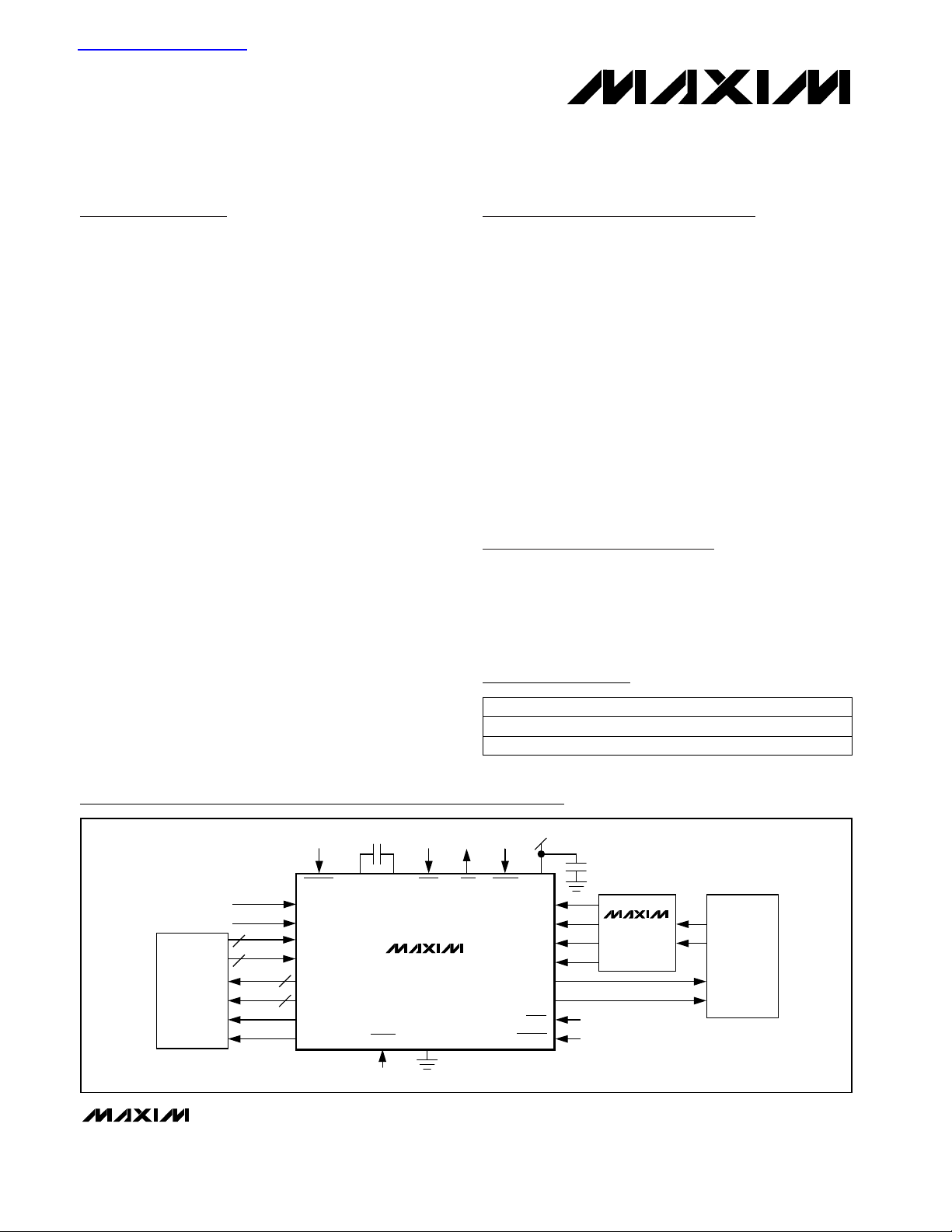
Typical Application Circuit
Ordering Information
PART
MAX3831UCB
MAX3832UCB
0°C to +85°C
0°C to +85°C
TEMP. RANGE PIN-PACKAGE
64 TQFP-EP
64 TQFP-EP
Pin Configuration appears at end of data sheet.
查询MAX3831供应商
PLBEN
+3.3V
V
SCLKI-
SCLKI+
SDI-
SDI+
SDO+
SDO-
LBEN
RSETFR
0.1µF
CC
CML
CML
MAX3876
2.5Gbps
CDR
TTL
TTL
2.5Gbps
OPTICAL
TRANSCEIVER
TTL
RSETES
155MHz REF
CLOCK INPUT
CMOS
OVERHEAD
LVDS
4
LVDS
4
LVDS
LVDS
RCLKI+
RCLKIPDI1+ TO PDI4+
PDI1- TO PDI4-
4
PDO1+ TO PDO4+
4
PDO1- TO PDO4-
PCLKO+
PCLKO-
0.33µF
FIL+ FIL-
TRIEN
MAX3831
MAX3832
TTL
TTL TTL TTL
TEST
LOF
GND
MAX3831/MAX3832
+3.3V, 2.5Gbps, SDH/SONET, 4-Channel
Interconnect Mux/Demux ICs with Clock Generator
2 _______________________________________________________________________________________
ABSOLUTE MAXIMUM RATINGS
DC ELECTRICAL CHARACTERISTICS
(VCC= +3.0V to +3.6V, LVDS differential load = 100Ω ±1%, CML load = 50Ω ±1% to VCC, all TTL inputs are open, TA= 0°C to
+85°C, unless otherwise noted. Typical values are at T
A
= +25°C and VCC= +3.3V.)
Stresses beyond those listed under “Absolute Maximum Ratings” may cause permanent damage to the device. These are stress ratings only, and functional
operation of the device at these or any other conditions beyond those indicated in the operational sections of the specifications is not implied. Exposure to
absolute maximum rating conditions for extended periods may affect device reliability.
Positive Supply Voltage (VCC)...............................-0.5V to +5.0V
Input Voltage (LVDS, TTL)..........................-0.5V to (V
CC
+ 0.5V)
CML Input Voltage ..........................(V
CC
- 0.8V) to (VCC+ 0.5V)
FIL+, FIL- Voltage.......................................-0.5V to (V
CC
+ 0.5V)
TTL Output Voltage ....................................-0.5V to (V
CC
+ 0.5V)
LVDS Output Voltage ..................................-0.5V to (V
CC
+0.5V)
CML Output Currents..........................................................22mA
Continuous Power Dissipation (T
A
= +85°C) (Note 1)
64-Pin TQFP-EP (derate 40.0mW/°C above +85°C) .........2.6W
Operating Temperature Range...............................0°C to +85°C
Storage Temperature Range .............................-60°C to +150°C
Lead Temperature (soldering, 10sec) .............................+300°C
Short outputs together (Note 3)
TRIEN = V
CC
TRIEN = GND
Figure 1
LVDS input, VOS= 1.2V
CONDITIONS
V
VCC- VCC+
0.6 0.4
V
IS
Single-Ended Input Voltage Range
VVCC- 0.2Output Common-Mode Voltage
Ω85 100 115Differential Output Impedance
mVp-p640 800 1000V
ODp-p
Differential Output Voltage
mA12Output Current
Ω80 120
Differential Output Impedance
MΩ>1
mV±25
∆VOS
Change in Magnitude of Output
Offset Voltage for Complementary
States
V1.125 1.275V
OS
Output Offset Voltage
mV±25
∆VOD
Change in Magnitude of
Differential Output Voltage for
Complementary States
mA
440 580
I
CC
Supply Current
mV250 400
VOD
Differential Output Voltage
V0.925V
OL
Output Voltage Low
V1.475V
OH
Output Voltage High
µA270I
OS
Input Common-Mode Current
mV0 2400V
IN
Input Voltage Range
mV-100 +100V
IDTH
Differential Input Threshold
mV90V
HYST
Threshold Hysteresis
Ω85 100 115R
IN
Input Impedance
UNITSMIN TYP MAXSYMBOLPARAMETER
Figure 2
Ω85 100 115Differential Input Impedance
mVp-p400 1200Differential Input Voltage Swing
LVDS INPUTS AND OUTPUTS
CML INPUTS AND OUTPUTS
Note 1: Based on empirical data from the MAX3831/MAX3832 evaluation kit.
CML inputs and outputs open,
LVDS input VOS= 1.2V (Note 2)
MAX3831
MAX3832 480 614
MAX3831/MAX3832
+3.3V, 2.5Gbps, SDH/SONET, 4-Channel
Interconnect Mux/Demux ICs with Clock Generator
_______________________________________________________________________________________ 3
DC ELECTRICAL CHARACTERISTICS (continued)
(VCC= +3.0V to +3.6V, LVDS differential load = 100Ω ±1%, CML load = 50Ω ±1% to VCC, all TTL inputs are open, TA= 0°C to
+85°C, unless otherwise noted. Typical values are at T
A
= +25°C and VCC= +3.3V.)
AC ELECTRICAL CHARACTERISTICS
(VCC= +3.0V to +3.6V, LVDS differential load = 100Ω ±1%, CML load = 50Ω ±1% to VCC, all TTL inputs are open, TA= 0°C to
+85°C, unless otherwise noted. Typical values are at T
A
= +25°C and VCC= +3.3V.) (Note 4)
TRIEN = GND
IOL= 2mA
IOH= 20µA
VIH= 2.0V
VIL= 0
CONDITIONS
kΩ6Output Impedance
V0.4V
OL
Output Voltage Low
V2.4V
OH
Output Voltage High
V2.0V
IH
Input Voltage High
V0.8V
IL
Input Voltage Low
µA-250 -50I
IH
Input Current High
µA-550 -100I
IL
Input Current Low
UNITSMIN TYP MAXSYMBOLPARAMETER
Note 2: When TEST = GND, the pattern generator will consume an additional 30mA.
Note 3: Guaranteed by design and characterization.
(Note 7)
(Note 5)
20% to 80%
CONDITIONS
ps
p-p
818SDJ
Serial-Data Output Deterministic
Jitter
ps
RMS
3.5
Mbps622.08Parallel Input Data Rate
ns±7.5t
es
Maximum Parallel Input Skew
Gbps2.48832Serial-Data Output Rate
ps120tr, t
f
Serial-Data Output Rise/Fall Time
UNITSMIN TYP MAXSYMBOLPARAMETER
Figure 3
Figure 3
Mbps622.08PDO±Parallel-Data Output Rate
Gbps2.48832Serial-Data Input Rate
ps100t
SU
Serial-Data Setup Time
ps100t
H
Serial-Data Hold Time
(Note 6)
ps
p-p
40
SRJSerial-Data Output Random Jitter
TTL INPUTS AND OUTPUTS
MAX3831
PCLKO±Parallel-Clock Output Frequency MHz
622.08
MAX3831, Figure 3t
CLK-Q
PCLKO to PDO_ Delay ps-100 90 300
Any differential pairt
SKEW1
LVDS Differential Skew ps65
PDO1± to PDO4±t
SKEW2
LVDS Channel-to-Channel Skew ps<100
LVDS Three-State Enable Time ns30
Note 4: AC characteristics are guaranteed by design and characterization.
Note 5: Relative to the positive edge of the 155MHz reference clock. PDI1 to PDI4 aligned to RCLKI at reset.
Note 6: Measured with a reference clock jitter of <1ps
RMS
.
Note 7: Deterministic jitter is the arithmetic sum of pattern-dependent jitter and pulse-width distortion.
MAX3832 155.52
20% to 80%LVDS Output Rise/Fall Time ps350
4:1 MULTIPLEXER WITH CLOCK GENERATOR
1:4 DEMULTIPLEXER
MAX3831/MAX3832
+3.3V, 2.5Gbps, SDH/SONET, 4-Channel
Interconnect Mux/Demux ICs with Clock Generator
4 _______________________________________________________________________________________
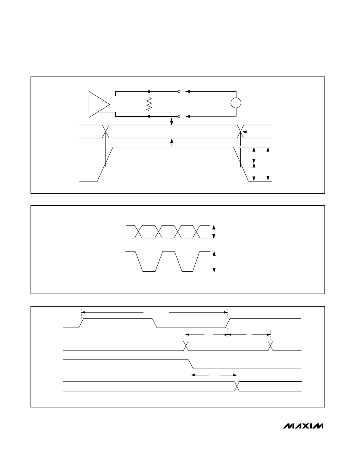
Figure 1. Definition of the LVDS Output
Figure 2. Definition of the CML Input
Figure 3. Timing Parameters
PDO+
V
D
PDO-
V
PDO-
SINGLE-ENDED OUTPUT
V
PDO+
DIFFERENTIAL OUTPUT
0V (DIFF)
R
= 100Ω
L
V
|
OD|
V
OD
V
OH
V
OS
V
OL
+V
OD
0V
V
= V
PDO+
- V
PDO-
ODp-p
-V
OD
SCLKI
SDI
PCLKO
PDO1–PDO4
SDI+
SDI-
(SDI+) - (SDI-)
t
SCLK
= 1 / f
SCLK
V
ID
t
SU
t
CLK-Q
200mV MIN
600mV MAX
400mVp-p MIN
1200mVp-p MAX
t
H
NOTE: SIGNAL SHOWN IS DIFFERENTIAL. FOR EXAMPLE, SCLKI = (SCLKI+) - (SCLKI-).
MAX3831/MAX3832
+3.3V, 2.5Gbps, SDH/SONET, 4-Channel
Interconnect Mux/Demux ICs with Clock Generator
_______________________________________________________________________________________ 5
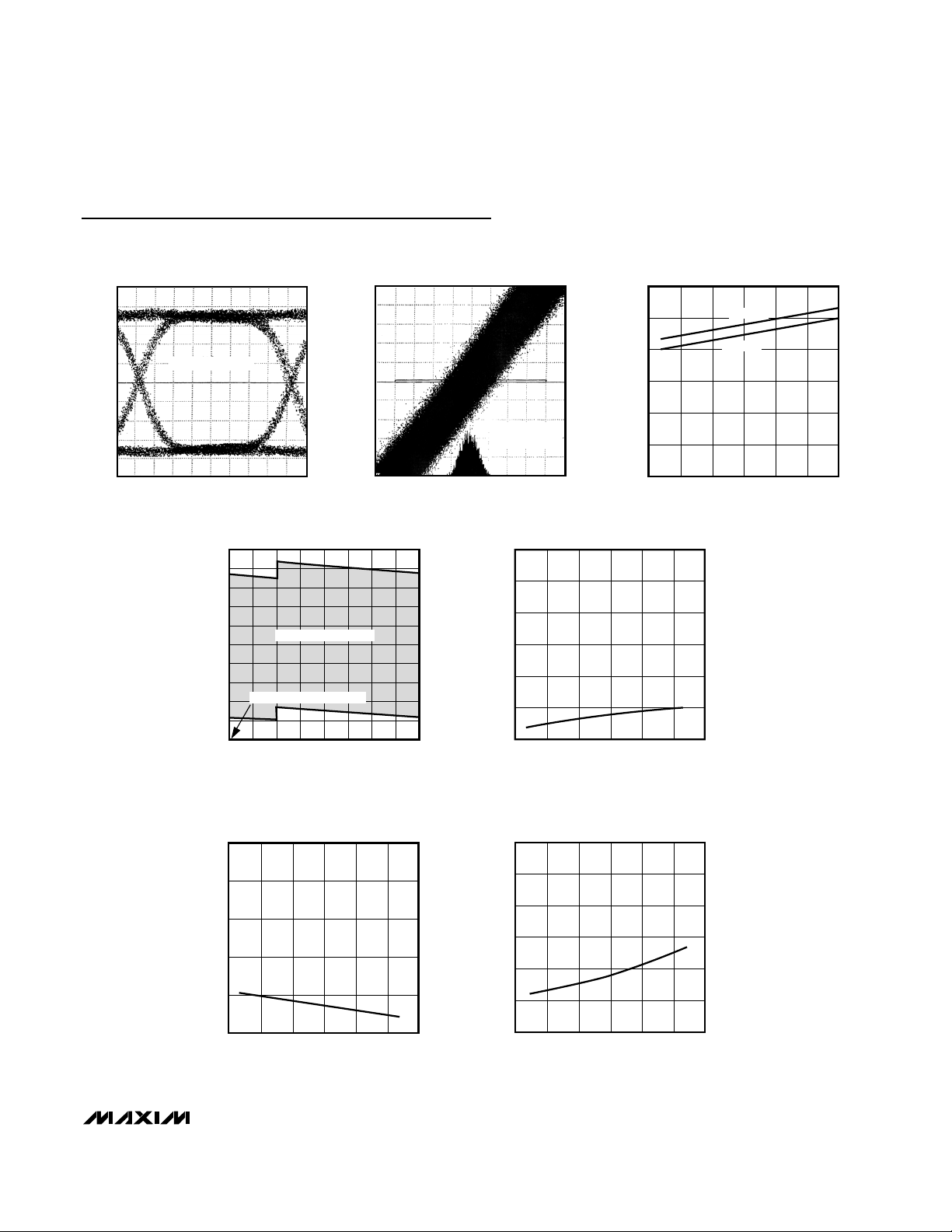
Typical Operating Characteristics
(VCC= +3.3V, TA = +25°C, unless otherwise noted.)
SERIAL-DATA OUTPUT EYE DIAGRAM
MAX3831/2 toc01
223-1 PRBS PATTERN
50ps/div
ELASTIC STORE RANGE
10
8
6
4
2
0
-2
-4
-6
-8
VARIATION OF DATA DELAY AFTER RESET (ns)
-10
0 0.4 0.60.2 0.8 1.0 1.2 1.4 1.6
ERROR-FREE OPERATION
CHANNEL ALIGNED TO RCLKI
DATA TO RCLKI DELAY AT RESET (ns)
SERIAL-DATA OUTPUT JITTER
WIDEBAND RMS
JITTER = 2.48ps
5ps/div
100
MAX3831/2 toc04
80
60
40
HOLD TIME (ps)
20
0
-20
-50 0 25-25 50 75 100
SUPPLY CURRENT vs. TEMPERATURE
600
MAX3831/2 toc02
500
400
300
200
SUPPLY CURRENT (mA)
100
0
-50 0 25-25 50 75 100
SERIAL-DATA HOLD TIME
TEMPERATURE (°C)
MAX3832
MAX3831/2 toc03
MAX3831
TEMPERATURE (°C)
MAX3831/2 toc05
PARALLEL CLOCK-TO-DATA OUTPUT
MAX3831
SERIAL-DATA SETUP TIME
100
80
60
40
SETUP TIME (ps)
20
0
-50 0 25-25 50 75 100
TEMPERATURE (°C)
MAX3831/2 toc06
PROPAGATION DELAY vs. TEMPERATURE
300
250
200
150
100
50
PCLKO TO PDO_ PROPAGATION DELAY (ps)
0
-50 0 25-25 50 75 100
TEMPERATURE (°C)
MAX3831/2 toc07

MAX3831/MAX3832
+3.3V, 2.5Gbps, SDH/SONET, 4-Channel
Interconnect Mux/Demux ICs with Clock Generator
6 _______________________________________________________________________________________
7
Self-Test Enable. When this TTL input is forced low, the built-in pattern generator generates
a standard OC-12 SONET-like frame of 12 A1s, 12 A2s, and 9696 bytes of 2
7
- 1 pseudo-
random bits. This also enables an internal serial-system-loopback path. The CML inputs
(SDI± and the SCLK±) and the LVDS inputs are ignored in this mode. An internal 15kΩ pullup resistor pulls TEST high for normal operation.
TEST
9
8 Positive CML Serial-Data Input, 2.488GbpsSDI+
Negative CML Serial-Data Input, 2.488GbpsSDI-
12
11 Positive CML Serial-Clock Input, 2.488GHzSCLKI+
Negative CML Serial-Clock Input, 2.488GHzSCLKI-
15
14 Negative LVDS Parallel-Clock Output, 622.08MHz (MAX3831); 155.52MHz (MAX3832)PCLKO-
Positive LVDS Parallel-Clock Output, 622.08MHz (MAX3831); 155.52MHz (MAX3832)PCLKO+
30
18–23, 26, 27 No ConnectionN.C.
Frame Reset. When this TTL input is forced low, the frame detector and pattern generator
are reset. The LOF output is also asserted low. An internal 15kΩ pull-up resistor pulls
RSETFR high for normal operation.
RSETFR
33
31 TTL Loss-of-Frame Output. Asserts low in a loss-of-frame condition.
LOF
3-State Enable. When this TTL input is forced low, all TTL and LVDS outputs go into a highimpedance state. An internal 15kΩ pull-up resistor pulls TRIEN high for normal operation.
TRIEN
35, 37, 40, 42
34, 36, 39, 41 Negative LVDS Parallel-Data Output, 622MbpsPDO4- to PDO1-
Positive LVDS Parallel-Data Output, 622MbpsPDO4+ to PDO1+
45, 47, 51, 53
44, 46, 50, 52 Negative LVDS Parallel-Data Input, 622MbpsPDI4- to PDI1-
Positive LVDS Parallel-Data Input, 622MbpsPDI4+ to PDI1+
54
Parallel System Loopback Enable. When this TTL input is forced low, the LVDS parallel
inputs route through the elastic store to the LVDS parallel outputs. This bypasses the highspeed mux and demux. An internal 15kΩ pull-up resistor pulls PLBEN high for normal operation.
PLBEN
PIN FUNCTIONNAME
6
Line Loopback Enable. When this TTL input is forced low, the CML serial-data inputs (SDI±)
route directly to the CML serial-data outputs (SDO±). No other inputs or outputs are affected.
An internal 15kΩ pull-up resistor pulls LBEN high for normal operation. See Test Loopbacks.
LBEN
4 Positive CML Serial-Data Output, 2.488GbpsSDO+
3 Negative CML Serial-Data Output, 2.488GbpsSDO-
2, 5, 10, 13,
17, 24, 38, 55,
59, 64
+3.3V Supply VoltageV
CC
1, 16, 25, 28,
29, 32, 43, 48,
49, 60, 63
Supply GroundGND
Pin Description
56 Negative LVDS Reference Clock Input, 155.52MHz RCLKI-
57 Positive LVDS Reference Clock Input, 155.52MHzRCLKI+

_______________Detailed Description
The MAX3831/MAX3832 use a 4:1 mux and 1:4 demux
with an elastic store buffer to simplify SDH/SONET
interconnect I/O routing. The 622Mbps low-voltage differential signal (LVDS) parallel inputs pass through the
10-bit elastic store buffer, which accommodates ±7.5ns
skew on any single input relative to the 155MHz reference clock input RCLKI. This reference clock is
required to synthesize the internal 2.488GHz clock
used to drive the elastic store and 4:1 multiplexer. All
TTL and LVDS outputs can be placed in a high-impedance state. See Figure 4 for a functional diagram.
The 4:1 mux bit-interleaves the parallel data, providing
a 2.488Gbps CML serial output to the optical or electrical driver. The CML serial input receives the
2.488Gbps data, the demux deinterleaves it to
622Mbps and sends the data to the frame detector.
The frame detector monitors one 622Mbps channel and
rolls the demux into the proper channel assignment.
The MAX3831/MAX3832 include high-speed, built-in
self-test (BIST), which also allows testing of the
622Mbps parallel-system loopback and the 2.488Gbps
line loopback.
Elastic Store Buffer
Each parallel-data input, PDI1 to PDI4, passes through
its respective 10-bit elastic store buffer. Following an
elastic store reset, this buffer accommodates ±7.5ns of
skew on any input relative to the 155MHz reference
clock. Figure 5 illustrates the elastic store buffer relationship with RCLKI. The Elastic Store Range graph in
the Typical Operating Characteristics shows the
amount of data skew tolerated.
Following a 10µs power-up period, the locations of the
individual data-channel bit transitions are acquired,
guaranteeing data preservation. The output of this
block passes directly into the 4:1 mux. After power-up,
the elastic store buffer must be reset by applying a low
pulse on RSETES for at least 10ns.
Due to the inherent uncertainty of the data transitions
between the parallel-data inputs there is no bit or frame
alignment between these inputs. However, the demux
ensures proper channel assignment is maintained.
Bit-Interleaved Multiplexer/
Demultiplexer
The MAX3831/MAX3832 use a bit interleave/deinterleave
mux/demux. To guarantee channel assignment, one of
the four channels is inverted before multiplexing to provide a reference for the frame detector during demultiplexing. After demultiplexing, the same channel is
inverted back to the original data format.
Frame Detector
After a 2.5Gbps serial data is bit deinterleaved into four
622Mbps channels, an SDH/SONET frame detector
monitors the fourth channel, looking for the 32-bit pattern (A1A1A2A2) in the OC-12 header. To maintain correct channel assignment, the demux outputs rotate until
this 32-bit overhead pattern is reliably detected. A lossof-frame output, LOF, indicates when the received data
is in or out of frame. When LOF goes high, the frame
pattern is detected and the demux outputs are correctly assigned. When LOF is low, the frame detection circuitry is searching for the correct frame. A RSETFR
(TTL, active low) is included to reset the frame detector
when necessary.
The frame detector uses an algorithm to detect an inframe condition and a loss-of-frame condition; this algorithm is implemented to meet the SONET in-frame and
false-frame specs. The frame_search state will occur
upon start-up or reset. In this state, the frame detector
scans through the incoming serial data searching for the
framing pattern in the channel 4 output of the demux.
While in this state, if the framing pattern is not found
within 250µs, the demux channels are shifted (rolled)
and the frame search continues (Figure 6).
In-frame will be declared if two consecutive framing
patterns are found at the correct byte locations within
the SONET frame (9720 bytes). If this pattern is not pre-
MAX3831/MAX3832
+3.3V, 2.5Gbps, SDH/SONET, 4-Channel
Interconnect Mux/Demux ICs with Clock Generator
_______________________________________________________________________________________________________ 7
Pin Description (continued)
PIN FUNCTIONNAME
58
Elastic Store Reset. The elastic buffer is centered on a rising edge of RSETES, maximizing
the elastic store range. Data must be present for 10µs before applying a pulse of at least
10ns. An internal 15kΩ pull-up resistor pulls RSETES high for normal operation.
RSETES
62
61 Negative PLL Filter Capacitor Input. Connect a 0.33µF capacitor between FIL+ and FIL-.FIL-
Positive PLL Filter Capacitor Input. Connect a 0.33µF capacitor between FIL+ and FIL-.FIL+
EP
Ground. This must be soldered to a circuit board for proper thermal performance (see
Package Information).
Exposed Paddle

MAX3831/MAX3832
sent at the correct location (false frame), the state
machine will return to the frame_search state described
above. While in the in_frame state, each frame will be
checked for a framing pattern at the correct location.
Four consecutive false frames will cause the state
machine to return to the frame_search state described
above. The false-frame counter is reset with three or
fewer consecutive false frames.
Built-In Self-Test
with On-Chip Serial Loopback
An on-chip pattern generator can be enabled to produce a 622Mbps SDH/SONET-like transport overhead
followed by a pseudorandom bit sequence. This consists
of 12 A1s, 12 A2s, and a pseudorandom bit stream
(PRBS = 2
7
- 1). When TEST is low, this pattern is distrib-
uted to all parallel inputs, bypassing the LVDS input
buffers. Note, this pattern is skewed by one 622MHz
+3.3V, 2.5Gbps, SDH/SONET, 4-Channel
Interconnect Mux/Demux ICs with Clock Generator
Figure 5. Example of Elastic Store Function
8 _______________________________________________________________________________________
Figure 4. Functional Diagram
622MHz
2.488Gbps
2.488GHz
TRIEN
GENERATOR
MAX3831
MAX3832
LINE LOOPBACK
TEST
CLOCK
2.488Gbps
SYSTEM LOOPBACK
LBEN
SDO+
SDO-
SDI+
SDI-
SCLKI+
SCLKI-
(155MHz)
RCLKI+
LVDS
RCLKI-
PDI1+
LVDS
PDI1-
PDI2+
LVDS
PDI2-
PDI3+
LVDS
PDI3-
PDI4+
LVDS
PDI4-
PDO1+
LVDS
PDO1-
*MAX3831: f
PDO2+
LVDS
PDO2-
PDO3+
LVDS
PDO3-
PDO4+
LVDS
PDO4-
PLBEN
PCLKO+
LVDS
PCLKO-
= 622MHz, MAX3832: f
PCLKO
*
PCLKO
PATTERN
GENERATOR
= 155MHz
TEST
RSETES
155MHz
622MHz
ES
ES
ES
ES
622Mbps PARALLEL LOOPBACK
FRAME
DETECTOR
RSETFR
FREQUENCY
GENERATOR
2.488GHz
LOF
CK
4:1
MUX
1:4
DEMUX
ROTATE
FIL-FIL+
D
CK
D0
-t
es
C0 C1
D0 D1
DATA INPUT
≥10ns
+t
es
B1 B2
PDI2
PDI3
PDI4
RSETES
RCLKI
PDI1
PDI2
PDI3
PDI4
DATA OUTPUT OF ELASTIC STORE
A1
B2B0
C1
DATA OUTPUT OF ELASTIC STORE
A0 A1
A0A0PDI1
B1B1
C0C0
D1D1
A0
B1
C0
D1
AT t = t
AT t > t
o
o

MAX3831/MAX3832
+3.3V, 2.5Gbps, SDH/SONET, 4-Channel
Interconnect Mux/Demux ICs with Clock Generator
_______________________________________________________________________________________ 9
Figure 6. Frame Detection Flow Diagram
FRAME DETECT
START-UP OR RESET
START 250µs TIMER
FRAME_SEARCH
LOF = 0
FRAME
PATTERN
DETECTED?
YES
1 FRAME DETECTED
RESET BYTE
AND FRAME
NO
TIMER
TIMED OUT?
NO
YES
ROLL DATA
FRAME
PATTERN
DETECTED?
YES
IN_FRAME
LOF = 1
FRAME
PATTERN
DETECTED?
YES
NO
NO
FRAME
PATTERN
DETECTED?
NO
FRAME
PATTERN
DETECTED?
NO
NO
FRAME
PATTERN
DETECTED?
YES
YES
YES

MAX3831/MAX3832
+3.3V, 2.5Gbps, SDH/SONET, 4-Channel
Interconnect Mux/Demux ICs with Clock Generator
10 ______________________________________________________________________________________
clock cycle between each channel. In this test mode, serial data is internally looped back to the demux. All frame
detect logic is exercised using this mode. The CML
inputs (SDI± and SCLKI±) and LVDS inputs (PDI_±) are
ignored in this mode. After the BIST mode is enabled, the
loss-of-frame flag LOF goes high, indicating that the selftest has passed. In normal operation, TEST is left open
(internally pulled high), disabling the pattern generator
and accepting data from the parallel input channels.
Test Loopbacks
Two additional test loopbacks are provided: parallel
system loopback and serial line loopback.
Parallel System Loopback
In parallel system loopback, four 622Mbps parallel
input channels are phase aligned by an associated 10bit elastic store and routed to the output LVDS buffers.
This loopback is controlled by setting PLBEN low.
Normal data transmission is resumed when PLBEN
goes high (internally pulled high).
Serial Line Loopback
Serial line loopback is used for testing the performance
of the optical transceiver and the transmission link. The
received 2.488Gbps data stream is routed to the transmit CML output buffer. Line loopback is enabled when
LBEN is asserted low. When LBEN is left open (internally
pulled high), normal serial-data transmission resumes.
LVDS Parallel Interface
The MAX3831 parallel interface includes four OC-12
data inputs, a 155MHz reference clock input, four
622Mbps parallel-data outputs, and a 622MHz parallelclock output (MAX3832, f
PCLKO
= 155MHz). All parallel
inputs and outputs are LVDS compatible to minimize
power dissipation, speed transition time, and improve
noise immunity. The 155MHz input signal at RCLKI
requires a duty cycle between 40% and 60%.
The LVDS outputs go into a high-impedance state when
TRIEN is forced low. This simplifies system checks by
allowing vectors to be forced on the LVDS outputs.
CML Serial Interface
The MAX3831/MAX3832 provide a 2.488Gbps serialdata stream to a driver and accept 2.488Gbps serial
data and a 2.488GHz clock signal from an external
clock and data recovery device (MAX3876). The highspeed interface is CML compatible, resulting in lower
system power dissipation and excellent performance
(Figure 7).
__________Applications Information
Low-Voltage Differential
Signal Inputs/Outputs
The MAX3831/MAX3832 have LVDS inputs and outputs
for interfacing with high-speed digital circuitry. All LVDS
inputs and outputs are compatible with the IEEE-1596.3
LVDS specification. This technology uses 250mV to
400mV differential low-voltage amplitudes to achieve
fast transition times, minimize power dissipation, and
improve noise immunity.
For proper operation, the parallel clock and data LVDS
outputs (PCLKO+, PCLKO-, PDO_+, PDO_-) require
100Ω differential DC termination between the inverting
and noninverting outputs. Do not terminate these outputs to ground. The parallel-data LVDS inputs (PDI_+,
PDI_-) are internally terminated with 100Ω differential
input resistance and therefore do not require external
termination.
Interfacing with PECL/ECL
Input Levels
When interfacing with differential PECL input levels, it is
important to attenuate the signal while still maintaining
50Ω termination (Figures 8 and 9). Observe the common-mode input voltage specifications. AC-coupling is
required if a VCCother than 3.3V is used to maintain the
input common-mode level (Figure 8).
Figure 7. CML-to-CML Interface
V
V
CC
50Ω
50Ω
SDO+
SDO-
MAX3876
CC
50Ω
50Ω
SDI+
SDI-
MAX3831
MAX3832

MAX3831/MAX3832
+3.3V, 2.5Gbps, SDH/SONET, 4-Channel
Interconnect Mux/Demux ICs with Clock Generator
______________________________________________________________________________________ 11
Figure 8. PECL-to-CML Interface Figure 9. Direct Coupling of a PECL Output into the MAX3831/
MAX3832
Layout Techniques
For best performance, use good high-frequency layout
techniques. Filter voltage supplies, keep ground connections short, and use multiple vias where possible.
Use controlled-impedance transmission lines to interface with the MAX3831/MAX3832 high-speed inputs
and outputs.
Place power-supply decoupling as close to VCCas
possible. To reduce feedthrough, take care to isolate
the input signals from the output signals.
V
PECL
LEVELS
CC
50Ω
0.1µF
25Ω
SDI+
*
R
T
RT*
0.1µF
25Ω
100Ω
SDI-
50Ω
VCC = 3.3V
PECL
OUTPUT
82Ω
82Ω
82Ω
82Ω
SDI+
SDI-
= 3.3V
V
CC
50Ω
50Ω
MAX3831
MAX3832
MAX3831
MAX3832
SUCH THAT THE CORRECT PECL COMMON-MODE LEVEL
*SELECT R
T
IS ACHIEVED (TYPICAL PECL OUTPUT CURRENT = 14mA).

MAX3831/MAX3832
+3.3V, 2.5Gbps, SDH/SONET, 4-Channel
Interconnect Mux/Demux ICs with Clock Generator
12 ______________________________________________________________________________________
Pin Configuration
___________________Chip Information
TRANSISTOR COUNT: 14,134
TOP VIEW
CC
GND
FIL+
FIL-
GND
V
64
VCCRCLKI+
RSETES
5859606162 5455565763
RCLKI-
CC
PLBEN
V
PDI1+
PDI2+
PDI2-
PDI1-
5253
GND
49
5051
1
2
V
CC
SDO-
3
4
SDO+
5
V
CC
6
LBEN
7
TEST
8
SDI+
9
SDI-
10
V
CC
SCLKI+
11
12
SCLKI-
13
V
PCLKO-
PCLKO+
GND
CC
14
15
16
CC
V
N.C.
N.C.
N.C.
N.C.
MAX3831
MAX3832
2322212019 2726252418 2928 32313017
N.C.
N.C.
TQFP-EP
48 GNDGND
47
PDI3+
46
PDI3-
45
PDI4+
44
PDI4-
GND
43
PDO1+
42
PDO1-
41
PDO2+
40
PDO2-
39
V
38
CC
37
PDO3+
36
PDO3-
PDO4+
35
34
PDO4-
33
TRIEN
CC
V
GND
N.C.
N.C.
GND
GND
LOF
RSETFR
GND

MAX3831/MAX3832
+3.3V, 2.5Gbps, SDH/SONET, 4-Channel
Interconnect Mux/Demux ICs with Clock Generator
______________________________________________________________________________________ 13
Package Information
64L, TQFP.EPS

MAX3831/MAX3832
+3.3V, 2.5Gbps, SDH/SONET, 4-Channel
Interconnect Mux/Demux ICs with Clock Generator
14 ______________________________________________________________________________________
Package Information (continued)

MAX3831/MAX3832
+3.3V, 2.5Gbps, SDH/SONET, 4-Channel
Interconnect Mux/Demux ICs with Clock Generator
______________________________________________________________________________________ 15
NOTES

MAX3831/MAX3832
+3.3V, 2.5Gbps, SDH/SONET, 4-Channel
Interconnect Mux/Demux ICs with Clock Generator
Maxim cannot assume responsibility for use of any circuitry other than circuitry entirely embodied in a Maxim product. No circuit patent licenses are
implied. Maxim reserves the right to change the circuitry and specifications without notice at any time.
16 ____________________Maxim Integrated Products, 120 San Gabriel Drive, Sunnyvale, CA 94086 408-737-7600
© 1999 Maxim Integrated Products Printed USA is a registered trademark of Maxim Integrated Products.
NOTES
 Loading...