

Page 1
General Description
The MAX3815 cable equalizer automatically provides
compensation for DVI™, HDMI™, DFP, PanelLink®, and
ADC cables. It extends the usable cable distance up to
36 meters. The MAX3815 is designed to equalize signals encoded in the transition-minimized differential
signaling (TMDS
®
) format.
The MAX3815 features four CML-differential inputs and
outputs (three data and one clock). It provides a lossof-signal (LOS) output that indicates loss-of-clock signal. The outputs include a disable function or the
equalizer can be powered down to conserve power.
For direct chip-to-chip communication, the output drivers can be switched to one-half the DVI output specification to conserve power and reduce EMI. Equalization
can be automatic or set to manual control for specific
in-cable applications.
The MAX3815 is available in a 7mm x 7mm, 48-pin
TQFP-EP package and operates over a 0°C to +70°C
temperature range.
Applications
Front-Projector DVI/HDMI Inputs
High-Definition Televisions and Displays
DVI-D/HDMI Cable-Extender Modules and Active
Cable Assemblies
LCD Computer Monitors
Features
♦ Extends TMDS Cable Reach to Projectors or
Monitors Using DVI, DFP, PanelLink, ADC, or
HDMI Interfaces
♦ Extends TMDS Interface Length as Follows:
0 to 50 Meters Over DVI-Cable, 24 AWG STP
(Shielded-Twisted Pair)
0 to 36 Meters Over DVI-Cable, 28 AWG STP
0 to 30 Meters Over DVI-Cable, 30 AWG STP
♦ Compatible with DTV Resolutions 480i, 480p,
720p, 1080i, and 1080p
♦ Compatible with Computer Resolutions VGA,
SVGA, XGA, SXGA, UXGA
♦ Fully Automatic Equalization Up to 40dB at
825MHz (1.65Gbps), No System Control Required
♦ 3.3V Power Supply
♦ Power Dissipation of 0.6W (typ)
♦ 7mm x 7mm 48-Pin TQFP Lead-Free Package
MAX3815
TMDS Digital Video Equalizer for DVI/HDMI
Cables
________________________________________________________________
Maxim Integrated Products
1
Ordering Information
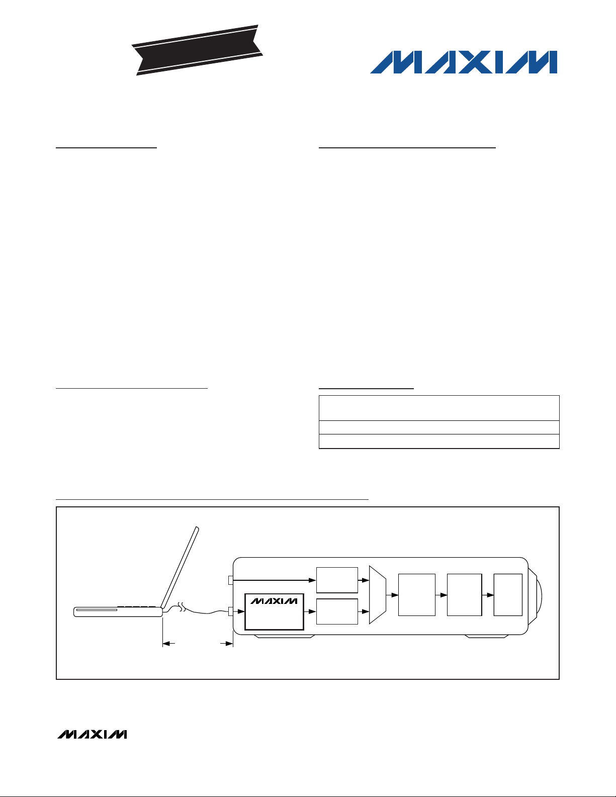
RGB/HV
ADC/SYNC
TMDS
DESERIALIZER
SELECT
IMAGE
SCALER AND
PROCESSOR
PANEL
INTERFACE
TIMING AND
DRIVERS
LCD,
DLP,
OR
LCOS
VGA INPUT
DVI-D INPUT
DVI-D CABLE UP
TO 36m OR 120ft
(28AWG STP)
LAPTOP
VIDEO PROJECTOR
MAX3815
EQUALIZER
Typical Application Circuits
19-3466; Rev 2; 2/08
For pricing, delivery, and ordering information, please contact Maxim Direct at 1-888-629-4642,
or visit Maxim’s website at www.maxim-ic.com.
EVALUATION KIT
AVAILABLE
+
Denotes lead-free package.
*EP = Exposed pad.
Typical Application Circuits continued at end of data sheet.
Pin Configuration appears at end of data sheet.
DVI is a trademark of Digital Display Working Group.
HDMI is a trademark of HDMI Licensing, LLC.
PanelLink and TMDS are registered trademarks of Silicon Image, Inc.
PART
MAX3815CCM 0°C to +70°C 48 TQFP-EP*
MAX3815CCM+ 0°C to +70°C 48 TQFP-EP* C48E-8
TEMP
RANGE
PINPACKAGE
C48E-8
PKG
CODE
Page 2
MAX3815
TMDS Digital Video Equalizer for DVI/HDMI
Cables
2 _______________________________________________________________________________________
ABSOLUTE MAXIMUM RATINGS
Stresses beyond those listed under “Absolute Maximum Ratings” may cause permanent damage to the device. These are stress ratings only, and functional
operation of the device at these or any other conditions beyond those indicated in the operational sections of the specifications is not implied. Exposure to
absolute maximum rating conditions for extended periods may affect device reliability.
Supply Voltage V
CC
..............................................-0.5V to +4.0V
Voltage at All I/O Pins.................................-0.5V to (V
CC
+ 0.7V)
Voltage between any CML I/O Complementary Pair ..........±3.3V
Continuous Power Dissipation (T
A
= +70°C)
48-Pin TQFP-EP (derate 36.2mW/°C above +70°C) ..2896mW
Operating Junction Temperature Range...........-55°C to +150°C
Storage Temperature Range .............................-55°C to +150°C
Die Attach Temperature...................................................+400°C
ELECTRICAL CHARACTERISTICS
(VCC= +3.0V to +3.6V, TA= 0°C to +70°C. Typical Values are at VCC= +3.3V, external terminations = 50Ω ±1%, TMDS rate =
250Mbps to 1.65Gbps, T
A
= +25°C, unless otherwise noted.)
PARAMETER SYMBOL CONDITIONS MIN TYP MAX UNITS
Power-Supply Current I
Supply-Noise Tolerance DC to 500kHz 200 mV
EQUALIZER PERFORMANCE
Residual Output Jitter (Cables
Only) 0.25Gbps to 1.65Gbps
(Notes 1, 2, and 3)
CID Tolerance 20 Bits
CONTROL AND STATUS
CLKLOS Assert Level
CML INPUTS (CABLE SIDE)
Differential Input Voltage Swing V
Common-Mode Input Voltage V
Input Resistance R
CML OUTPUTS (ASIC SIDE)
Differential Output-Voltage Swing V
Output-Voltage High Single-ended, OUTLEVEL = HIGH V
Output-Voltage Low Single-ended, OUTLEVEL = HIGH
Output Voltage During
Power-Down
CC
ID
CM
IN
OD
PWRDWN = HIGH 165 230
PWRDWN = LOW 10
1dB skin-effect loss at 825MHz 0.2
24dB skin-effect loss at 825MHz 0.2
40dB skin-effect loss at 825MHz 0.2
Differential peak-to-peak at EQ input with
165MHz clock
At cable input 800 1000 1400 mV
Single-ended 45 50 55 Ω
50Ω load, each side
to V
Single-ended, PWRDWN = LOW
CC OUTLEVEL = LOW 350 500 650
50 mV
V
-
CC
0.4
OUTLEVEL = HIGH 800 1000 1200
V
-
CC
600
V
-
CC
10
CC
V
V
CC
0.1
CC
400
V
CC
+10
+
-
mV
mA
P-P
UI
P-P
P-P
V
P-P
mV
mV
mV
Page 3
MAX3815
TMDS Digital Video Equalizer for DVI/HDMI
Cables
_______________________________________________________________________________________ 3
ELECTRICAL CHARACTERISTICS (continued)
(VCC= +3.0V to +3.6V, TA= 0°C to +70°C. Typical Values are at VCC= +3.3V, external terminations = 50Ω ±1%, TMDS rate =
250Mbps to 1.65Gbps, T
A
= +25°C, unless otherwise noted.)
Note 1: AC specifications are guaranteed by design and characterization.
Note 2: Cable input swing is 800mV to 1400mV differential peak-to-peak. Residual output jitter is defined as peak-to-peak determin-
istic jitter + 14.2 times random jitter.
Note 3: Test pattern is a 2
7
- 1 PRBS + 20 ones + 27- 1 PRBS (inverted) + 20 zeros.
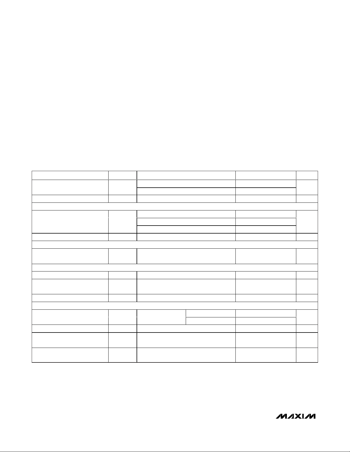
Typical Operating Characteristics
(Typical values are at VCC= +3.3V, TA= +25°C, data pattern = 27- 1 PRBS + 20 ones + 27- 1 PRBS (inverted) + 20 zeros, unless
otherwise noted.)
SUPPLY CURRENT
vs. TEMPERATURE
MAX3815 toc01
TEMPERATURE (°C)
SUPPLY CURRENT (mA)
605030 402010
110
120
130
140
150
160
170
180
190
200
100
070
OUTLEVEL = HIGH
OUTLEVEL = LOW
DIFFERENTIAL INPUT RETURN LOSS
vs. FREQUENCY
MAX3815 toc02
FREQUENCY (MHz)
GAIN (dB)
2500200015001000500
-45
-40
-35
-30
-25
-20
-15
-10
-5
0
-50
0 3000
EQUALIZER INPUT AFTER 205ft OF GORE 89
CABLE (TOP) EQUALIZER OUTPUT (BOTTOM)
MAX3815 toc03
5ns/div
128mV/div
350mV/div
DATA RATE = 1.65Gbps
40dB CABLE SKIN-EFFECT LOSS AT 825MHz
PARAMETER SYMBOL CONDITIONS MIN TYP MAX UNITS
Common-Mode Output Voltage
Rise/Fall Time (Note 1) 20% to 80% 80 130 200 ps
LVTTL CONTROL AND STATUS INTERFACE
LVTTL Input High Voltage V
LVTTL Input Low Voltage V
LVTTL Input High Current V
LVTTL Input Low Current GND < VIN < V
Open-Collector Output High
Open-Collector Output Low
Open-Collector Output Sink
50Ω load, each side to V
CC
OUTLEVEL = HIGH
IH
IL
< VIN < V
IH(MIN)
≥ 10kΩ to V
R
LOAD
R
≥ 2kΩ to V
LOAD
CC
IL(MAX)
CC
CC
,
V
CC
0.25
V
2.0 V
0.8 V
-50 µA
-100 µA
2.4 V
0.4 V
5mA
Page 4
MAX3815
TMDS Digital Video Equalizer for DVI/HDMI
Cables
4 _______________________________________________________________________________________
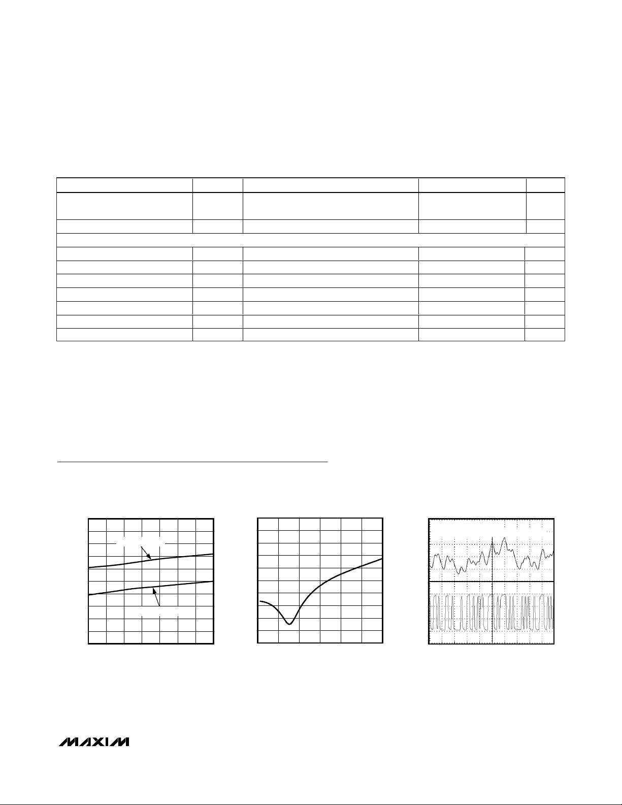
Typical Operating Characteristics (continued)
(Typical values are at VCC= +3.3V, TA= +25°C, data pattern = 27- 1 PRBS + 20 ones + 27- 1 PRBS (inverted) + 20 zeros, unless
otherwise noted.)
EQUALIZER INPUT EYE AFTER 205ft OF GORE 89
CABLE (TOP) EQUALIZER OUTPUT (BOTTOM)
MAX3815 toc04
152ps/div
350mV/div
DATA RATE = 1.65Gbps
40dB CABLE SKIN-EFFECT LOSS AT 825MHz
EQUALIZER INPUT EYE AFTER 205ft OF GORE 89
CABLE (TOP) EQUALIZER OUTPUT (BOTTOM)
MAX3815 toc05
1ns/div
300mV/div
DATA RATE = 250Mbps
40dB CABLE SKIN-EFFECT LOSS AT 825MHz
EQUALIZER EYES AFTER 100ft MADISON DIGITAL
FLAT-PANEL CABLE, 28 AWG (DATA RATE = 1.65Gbps)
MAX3815 toc06
200ps/div
350mV/div
EQUALIZER EYES AFTER 100ft MADISON DIGITAL
FLAT-PANEL CABLE, 28 AWG (DATA RATE = 350Mbps)
MAX3815 toc07
1ns/div
350mV/div
EQUALIZER EYES AFTER 3ft CABLE
(DATA RATE = 1.65Gbps)
MAX3815 toc08
200ps/div
350mV/div
JITTER vs. DATA RATE AFTER 205ft CABLE
WITH 40dB SKIN-EFFECT LOSS AT 825MHz
MAX3815 toc09
DATA RATE (Mbps)
JITTER (ps
P-P
)
14501250450 650 850 1050
20
40
60
80
100
120
0
250 1650
GORE 89 CABLE
RESIDUAL JITTER =
DJ + 14.2 x RJ
DETERMINISTIC JITTER
TOTAL JITTER vs. POWER-SUPPLY
NOISE FREQUENCY (DATA RATE = 1.65Gbps)
MAX3815 toc10
FREQUENCY (kHz)
TOTAL JITTER (ps
P-P
)
10,000100010 100
110
120
130
140
150
160
170
180
100
1 100,000
NOISE AMPLITUDE: 200mV
P-P
DATA THROUGH 100ft MADISON DIGITAL
FLAT-PANEL CABLE, 28AWG
0
0.2
0.1
0.4
0.3
0.5
0.6
0 10050 150 200
DETERMINISTIC JITTER vs. CABLE LENGTH
(TENSOLITE TWIN-AX 28 AWG)
MAX3815 toc11
CABLE LENGTH (ft)
DETERMINISTIC JITTER (UI
P-P
)
1.65Gbps
800Mbps
250Mbps
NO EQ
WITH
MAX3815 EQ
RESIDUAL JITTER vs. SIGNAL AMPLITUDE
INPUT TO CABLE (DATA RATE = 1.65Gbps)
MAX3815 toc12
DIFFERENTIAL AMPLITUDE (mV
P-P
)
RESIDUAL JITTER (ps
P-P
)
1.21.00.8
70
80
90
100
110
120
60
0.6 1.4
205ft OF GORE 89 CABLE WITH 40dB SKINEFFECT LOSS AT 825MHz
RESIDUAL JITTER = DJ + 14.2 X RJ
Page 5

MAX3815
TMDS Digital Video Equalizer for DVI/HDMI
Cables
_______________________________________________________________________________________
5
Typical Operating Characteristics (continued)
(Typical values are at VCC= +3.3V, TA= +25°C, data pattern = 27- 1 PRBS + 20 ones + 27- 1 PRBS (inverted) + 20 zeros, unless
otherwise noted.)
Pin Description
EQCONTROL VOLTAGE (RELATIVE TO VCC)
vs. CABLE LENGTH (MANUAL EQ CONTROL)
0
CABLE IS TENSOLITE TWIN-AX
-0.1
28 AWG WITH APPROXIMATELY
0.34dB OF LOSS PER FOOT AT
-0.2
825MHz
-0.3
-0.4
EQCONTROL VOLTAGE
-0.5
-0.6
-0.7
EQCONTROL VOLTAGE (V)
-0.8
-0.9
-1.0
04020 60 80 100 120
CABLE LENGTH (ft)
RESIDUAL JITTER
AT 1.65Gbps
MAX3815 toc13
200
180
160
)
140
P-P
120
100
200mV/div
80
60
RESIDUAL JITTER (ps
40
20
0
EQUALIZER OUTPUT EYE AFTER 120ft
OF CABLE (DATA RATE = 1.65Gbps)
CABLE IS TENSOLITE
TWIN-AX 28 AWG
100ps/div
MAX3815 toc14
LOSS-OF-CLOCK ASSERT THRESHOLD
vs. CABLE LENGTH
350
)
CABLE IS TENSOLITE TWIN-AX 28 AWG
P-P
300
250
200
165MHz CLOCK FREQUENCY
150
100
50
DIFFERENTIAL CLOCK AMPLITUDE (mV
0
0406020 80 100 120
25MHz CLOCK FREQUENCY
CABLE LENGTH (ft)
PIN NAME FUNCTION
1, 4, 5, 8, 9,
12, 13, 16,
38, 41, 43, 44
2 RX0_IN- Negative Data Input, CML
3 RX0_IN+ Positive Data Input, CML
6 RX1_IN- Negative Data Input, CML
7 RX1_IN+ Positive Data Input, CML
10 RX2_IN- Negative Data Input, CML
11 RX2_IN+ Positive Data Input, CML
14 RXC_IN+ Positive Clock Input, CML
15 RXC_IN- Negative Clock Input, CML
17 EQCONTROL
18 CLKLOS
19 PWRDWN
V
CC
Supply Voltage. All pins must be connected to VCC.
Equalizer Control. This pin allows the user to control the equalization level of the MAX3815. Connect
the pin to GND for automatic operation. Set the voltage to V
the voltage between V
- 1V to VCC for manual equalization. See the Typical Operating
CC
/ 2 for minimum equalization, or set
CC
Characteristics for more information.
Loss-of-Clock Signal Output, LVTTL Open Collector. This pin asserts low upon loss of the input TMDS
clock from the cable.
Power-Down Input, LVTTL. This input allows the IC to be powered down to conserve power. Connect
high for normal operation. Pull low for power-down mode.
MAX3815 toc15
Page 6

MAX3815
Detailed Description
The MAX3815 TMDS equalizer accepts differential CML
input data at rates of 250Mbps up to 1.65Gbps (individual channel data rate). It automatically adjusts to attenuation levels of up to 40dB at 825MHz due to
skin-effect losses in copper cable. It consists of four
CML input buffers, a loss-of-clock signal detector, three
independent adaptive equalizers, four limiting amplifiers, and four output buffers (Figure 1).
CML Input Buffers and Output Drivers
The input buffers and the output drivers are implemented using current-mode logic (CML) (see Figures 3 and
4). The output drivers are open-collector and can be
turned off with the OUTON pin, or can be set to output
a one-half amplitude signal (500mV
P-P
differential)
using the OUTLEVEL pin. For details on interfacing with
CML, refer to Maxim Application Note
HFAN-01.0:
Introduction to LVDS, PECL, and CML
.
Loss-of-Clock Signal Detector
The loss-of-clock signal detector indicates a loss-ofclock signal at the CLKLOS pin.
Adaptive Equalizer
The three data channels each contain an independent
adaptive equalizer. Each channel analyzes the incoming signal and determines the amount of equalization to
apply.
Limiting Amplifier
The limiting amplifier amplifies the signal from the
adaptive equalizer and truncates the top and bottom of
the waveform to provide a clean high- and low-level
signal to the output drivers.
Applications Information
Typical shielded twisted pair (STP) and unshielded
twisted pair (UTP) cables exhibit skin-effect losses,
which attenuate the high-frequency spectrum of a
TMDS signal, eventually causing data errors or even
closing the signal eye altogether given a long enough
cable. The MAX3815 recovers the data and opens the
signal eye through compensating equalization.
The basic TMDS interface is composed of four differential serial links: three links carry serial data up to
1.65Gbps each, and the fourth is a one-tenth-rate
(0.1x) clock that operates up to 165MHz. TMDS, as with
TMDS Digital Video Equalizer for DVI/HDMI
Cables
6 _______________________________________________________________________________________
Pin Description (continued)
PIN NAME FUNCTION
20, 23, 24,
25, 28, 29,
32, 33, 36,
37, 42
21 RXC_OUT- Negative Clock Output, CML
22 RXC_OUT+ Positive Clock Output, CML
26 RX2_OUT+ Positive Data Output, CML
27 RX2_OUT- Negative Data Output, CML
30 RX1_OUT+ Positive Data Output, CML
31 RX1_OUT- Negative Data Output, CML
34 RX0_OUT+ Positive Data Output, CML
35 RX0_OUT- Negative Data Output, CML
39 OUTLEVEL
40 OUTON
45–48 N.C. No Connection
EP Exposed Pad
GND Ground
Output-Level Control Input, LVTTL. This input sets the output amplitude to the standard DVI level
(1000mV
Output-Enable Control Input, LVTTL. This input enables the CML outputs when forced low and sets a
differential logic zero when forced high.
Ground. The exposed pad must be soldered to the circuit-board ground for proper
thermal and electrical operation.
) when high, and sets the output amplitude to 1/2 the DVI level (500mV
P-P
) when low.
P-P
Page 7

analog nVGA links, must handle a variety of resolutions
and screen update rates. The actual range of digital
serial rates is roughly 250Mbps to 1.65Gbps. For applications requiring ultra-high resolutions (e.g., QXGA), a
“double-link” TMDS interface is used and is composed
of six data links plus the clock, requiring two MAX3815
ICs with the clock going to both ICs. See Figure 2.
The MAX3815 can be used to extend any TMDS interface as used under the following trademarked names:
DVI (digital visual interface), DFP™ (digital flat-panel),
PanelLink, ADC™ (Apple display connector), and
HDMI (high-definition multimedia interface).
Loss-of-Clock Signal (
CLKLOS
) Output
Loss-of-clock signal is indicated by the CLKLOS out-
put. A low level on CLKLOS indicates that the signal
power on the RXC_IN pins has dropped below a
threshold. When there is sufficient input voltage to the
channel (typically greater than 100mV
P-P
differential),
CLKLOS is high. The CLKLOS output is suitable for
indicating problems with the transmission link caused
by, for example, a broken cable, a defective driver, or a
lost connection to the equalizer.
MAX3815
TMDS Digital Video Equalizer for DVI/HDMI
Cables
_______________________________________________________________________________________ 7
Figure 1. Functional Diagram
Figure 2. Connection Scheme for MAX3815 in Dual Link
Application
ADC is a trademark of Apple Computer, Inc.
DFP is a trademark of Video Electronics Standards Association
(VESA).
TERMINATED
RX2_IN+/-
RX1_IN+/-
RX0_IN+/-
RXC_IN+/-
3.3V CML
TERMINATED
3.3V CML
TERMINATED
3.3V CML
TERMINATED
3.3V CML
INPUT
BUFFER
INPUT
BUFFER
INPUT
BUFFER
INPUT
BUFFER
ADAPTIVE
EQ
ADAPTIVE
EQ
ADAPTIVE
EQ
LIMITING
AMPLIFIER
LIMITING
AMPLIFIER
LIMITING
AMPLIFIER
LIMITING
AMPLIFIER
DRIVER
DRIVER
DRIVER
DRIVER
RX2_OUT+/-
RX1_OUT+/-
RX0_OUT+/-
EQCONTROL
RXC_OUT+/-
CLKLOS
CLOCK LOS
DETECTOR
MAX3815
OUTON
OUTLEVEL
D0
D1
D2
D0
D1
D2
MAX3815
CLK
D3
D4
D5
MAX3815
CLK
D3
D4
D5
Page 8

MAX3815
A squelching function can be created by sending the
CLKLOS output through an inverter to the OUTON pin.
This will squelch the CML outputs whenever the clock
signal is removed. A loss-of-signal LED indicator can
be incorporated into the circuit as well (see Figure 3).
Output Level Control (OUTLEVEL) Input
The OUTLEVEL pin is an LVTTL input that allows the
user to select between standard output amplitude
(1000mV
P-P
differential) or one-half output amplitude
(500mV
P-P
differential). Forcing this pin high results in
the standard output signal level, and forcing this pin
low results in the reduced output signal level.
Equalizer Control (EQCONTROL) Input
The EQCONTROL pin allows the user to control the
equalization in one of three ways: forcing the pin to
ground sets the equalizer in automatic equalization
mode, forcing the pin to VCC/ 2 sets the equalizer to
minimum equalization, and forcing a voltage between
VCC- 1V to VCCallows manual control of the equalization level applied to the input signals. See the
Typical
Operating Characteristics
for more information.
Power-Down (
PWRDWN
) Input
The PWRDWN pin allows the part to be powered down
to reduce system power consumption. Force the pin
high for normal operation. Force the pin low to powerdown the IC. When powered down, the part consumes
approximately 10mA.
Output On (
OUTON
) Input
The OUTON pin is an LVTTL input. Force the pin low to
enable the outputs. Force the pin high to set a differential
zero on the outputs. When disabled, the outputs will go to
a differential zero, irrespective of the signal at the inputs.
Cable Selection
TMDS performance is heavily dependent on cable
quality. Deterministic jitter (DJ) can be caused by differential-to-common-mode conversion (or vice-versa)
TMDS Digital Video Equalizer for DVI/HDMI
Cables
8 _______________________________________________________________________________________
Figure 4. Simplified Input Circuit Schematic
Figure 5. Simplified Output Circuit Schematic
Interface Models
Figure 3. Squelch Circuit
V
10kΩ
CLKLOS
CC
4.7kΩ
LOSS-OF-CLOCK LED
OUTON
200Ω
MAX3815
V
CC
50Ω
RX_IN+/-
MAX3815
V
CC
RX_OUT+
RX_OUT-
Page 9

within a twisted pair (STP or UTP), usually a result of
cable twist or dielectric imbalance. Refer to Application
Note
HFAN-04.5.4: ‘Jitter Happens’ when a Twisted
Pair is Unbalanced
for more information.
Layout Considerations
The data and clock inputs are the most critical paths for
the MAX3815 and great care should be taken to minimize discontinuities on these transmission lines
between the connector and the IC. Here are some suggestions for maximizing the performance of the
MAX3815:
• The data and clock inputs should be wired directly
between the cable connector and IC without stubs.
• Input and output data channel designations are
only a guide. Polarity assignments can be swapped
and channel paths can be interchanged.
• An uninterrupted ground plane should be positioned beneath the high-speed I/Os.
• Ground-path vias should be placed close to the IC
and the input/output interfaces to allow a return current path to the IC and the DVI cable.
• Maintain 100Ω differential transmission line impedance into and out of the MAX3815.
• Use good high-frequency layout techniques and
multilayer boards with an uninterrupted ground
plane to minimize EMI and crosstalk.
Exposed-Pad Package
The exposed pad on the 48-pin TQFP-EP provides a
very low thermal resistance path for heat removal from
the IC. The pad is also electrical ground on the
MAX3815 and must be soldered to the circuit board
ground for proper thermal and electrical performance.
Refer to Maxim Application Note
HFAN-08.1: Thermal
Considerations of QFN and Other Exposed-Paddle
Packages
for additional information.
Chip Information
PROCESS: SiGe BiPOLAR
MAX3815
TMDS Digital Video Equalizer for DVI/HDMI
Cables
_______________________________________________________________________________________ 9
Figure 6. Cable Reach
Package Information
(For the latest package outline information, go to
www.maxim-ic.com/packages
.)
PACKAGE TYPE DOCUMENT NO.
48 TQFP
21-0065
TYPICAL MAX3815 CABLE REACH
60
50
40
30
20
CABLE LENGTH (meters)
10
LIMIT OF CABLE LENGTH WITHOUT EQ AT 1.65Gbps
5
32
AWG
SHADED AREA = MAX3815
USABLE CABLE LENGTH RANGE
AT ALL DVI RATES UP TO 1.65Gbps
TYPICAL DVI WIRE GAUGE RANGE
28
30
AWG
DVI WIRE GAUGE
26
AWG
AWG24AWG22AWG
Page 10

MAX3815
TMDS Digital Video Equalizer for DVI/HDMI
Cables
10 ______________________________________________________________________________________
Typical Application Circuits (continued)
MAX3815
1
2
3
4
5
6
7
8
9
10
11
12
36
35
34
33
32
31
30
29
28
27
26
25
13 14 15 16 17 18 19 20 21 22 23 24
48 47 46 45 44 43 42 41 40 39 38 37
V
CC
RX0_IN-
RX0_IN+
V
CC
V
CC
RX1_IN-
RX1_IN+
V
CC
V
CC
RX2_IN-
RX2_IN+
V
CC
N.C.
N.C.
N.C.
N.C.
VCCVCCGND
V
CC
OUTLEVEL
VCCGND
GND
RX0_OUT-
RX0_OUT+
GND
GND
RX1_OUT-
RX1_OUT+
GND
GND
RX2_OUT-
RX2_OUT+
GND
V
CC
RXC_IN+
RXC_IN-
V
CC
EQCONTROL
GND
RXC_OUT-
RXC_OUT+
GND
GND
CLKLOS
PWRDWN
OUTON
TOP VIEW
48 TQFP-EP
Pin Configuration
DVI-D OR HDMI
EXTENDER BOX
UP TO 36m
OF DVI-D OR
HDMI CABLE
(28 AWG)
MAX3816
DDC EXTENDER
STANDARD
LENGTH DVI-D
OR HDMI CABLE
HDTV
MAX3815
EQUALIZER
VIDEO SOURCE
DIGITAL BROADCAST
DIGITAL CABLE
DIGITAL SATELLITE
DVD
Blu-ray Disc™
Blu-ray Disc IS A TRADEMARK OF Blu-ray DISC ASSOCIATION.
Page 11

MAX3815
TMDS Digital Video Equalizer for DVI/HDMI
Cables
Maxim cannot assume responsibility for use of any circuitry other than circuitry entirely embodied in a Maxim product. No circuit patent licenses are
implied. Maxim reserves the right to change the circuitry and specifications without notice at any time.
Maxim Integrated Products, 120 San Gabriel Drive, Sunnyvale, CA 94086 408-737-7600 ____________________
11
© 2008 Maxim Integrated Products is a registered trademark of Maxim Integrated Products, Inc.
Revision History
REVISION
NUMBER
0 10/04 Initial release. —
1 8/05
2 2/08
REVISION
DATE
DESCRIPTION
Removed future status from the lead-free package in the Ordering Information
table.
Removed reference to the schematic and board layers in the Layout
Cons iderations section.
PAGES
CHANGED
1
9
 Loading...