

Page 1
General Description
The MAX3803 equalizer automatically provides compensation for transmission-medium losses encountered
with FR4 stripline and cable in an incredibly small 2mm
× 2.5mm package. It is ideal for backplane applications
requiring up to 40in between the line card and the
switch card or up to 10m of twin ax cable between
racks. Its small size provides placement and routing
flexibility. The CML inputs and outputs are DC-coupled
and can be terminated to a supply as low as +1.1V.
The MAX3803 operates from 0°C to +85°C and consumes 160mW at +3.3V.
Applications
Backplane Interconnect
Rack-to-Rack Interconnect
Common-Mode Voltage Translation
(LVDS, PECL, or CML)
Features
♦ DC-Coupled Input and Output to Terminations
as Low as +1.1V
♦ 2mm × 2.5mm UCSP
TM
♦ 1Gbps to 3.2Gbps Operating Range
♦ Spans 40in (1m) of FR4
♦ Spans 10m, 28AWG Twin Ax
♦ Receive Equalization to Reduce ISI
MAX3803
DC-Coupled, UCSP 3.125Gbps Equalizer
________________________________________________________________ Maxim Integrated Products 1
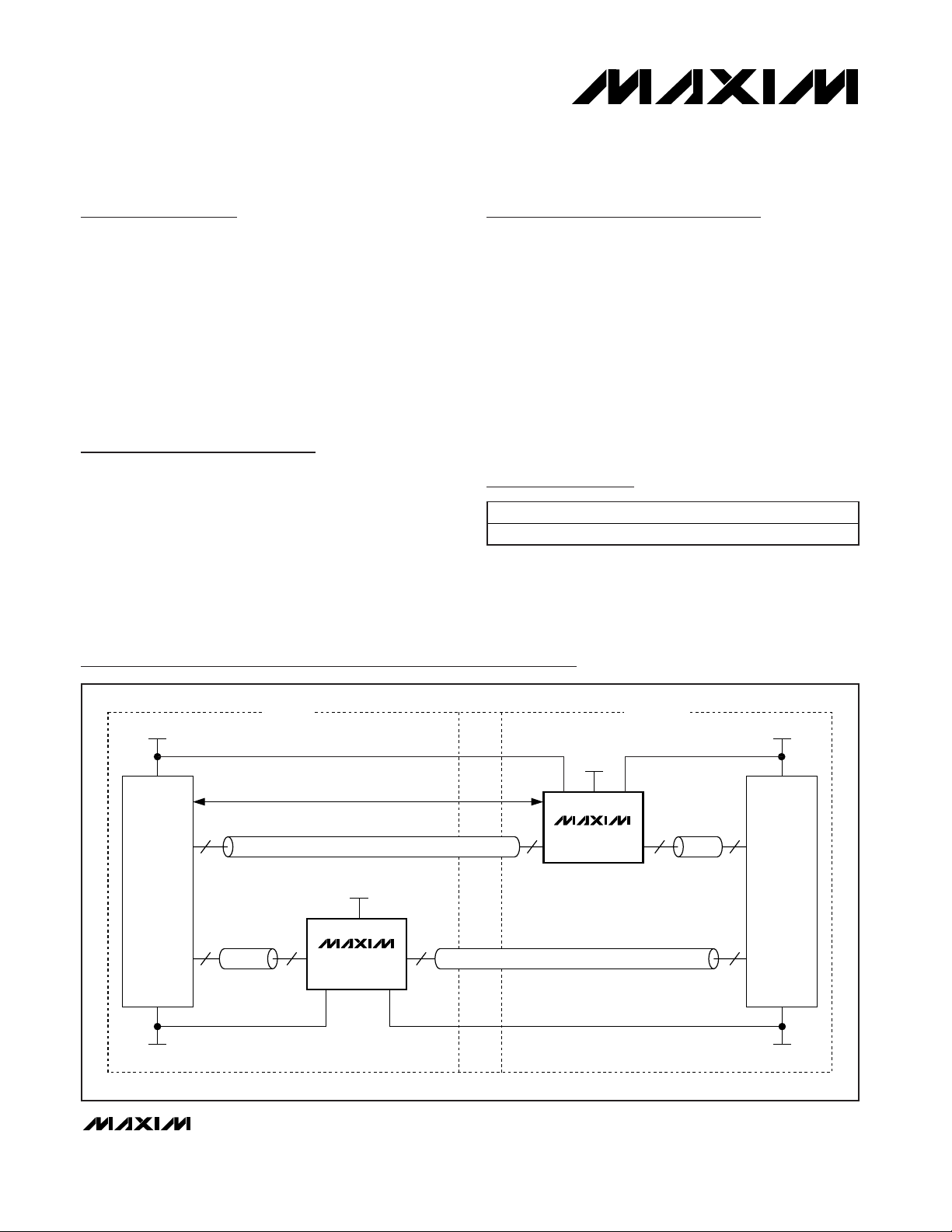
Ordering Information
MAC
WITH
SERDES
Rx Tx
Tx Rx
+1.1V ≤ V ≤ V
CC
+3.3V
+1.1V ≤ V ≤ V
CC
SWITCH
ASIC
WITH
SERDES
Rx
Tx
+1.1V ≤ V ≤ V
CC
+1.1V ≤ V ≤ V
CC
2222
IN
V
TIVCC
+3.3V
V
CC
V
TO
OUT
OUT
V
TO
V
TI
IN
22 22
≤40in (1m)
FR4 STRIPLINE
FR4 STRIPLINE
PC BOARD
BACKPLANE
LINE CARD SWITCH CARD
MAX3803
MAX3803
Typical Application Circuit
19-2699; Rev 1; 6/04
For pricing, delivery, and ordering information, please contact Maxim/Dallas Direct! at
1-888-629-4642, or visit Maxim’s website at www.maxim-ic.com.
Pin Configuration appears at end of data sheet.
UCSP is a trademark of Maxim Integrated Products, Inc.
PART TEMP RANGE PIN-PACKAGE
MAX3803UBP-T
0°C to +85°C 5 x 4 UCSP
Page 2
MAX3803
DC-Coupled, UCSP 3.125Gbps Equalizer
2 _______________________________________________________________________________________
ABSOLUTE MAXIMUM RATINGS
OPERATING CONDITIONS
Stresses beyond those listed under “Absolute Maximum Ratings” may cause permanent damage to the device. These are stress ratings only, and functional
operation of the device at these or any other conditions beyond those indicated in the operational sections of the specifications is not implied. Exposure to
absolute maximum rating conditions for extended periods may affect device reliability.
Supply Voltage, VCC, VTI, and VTO..........................-0.5V to +6V
Continuous Output Current ...............................-25mA to +25mA
IN±, OUT±, EN............................................-0.5V to (V
CC
+ 0.5V)
Operating Ambient Temperature Range ................0°C to +85°C
Storage Ambient Temperature Range...............-55°C to +150°C
PARAMETER
CONDITIONS
UNITS
Supply Voltage V
CC
3.0 3.3 3.6 V
Input Termination Voltage V
TI
1.1
V
Output Termination Voltage V
TO
1.1
V
10Hz ≤ f < 100Hz
100Hz ≤ f < 1MHz 40Supply Noise Tolerance
1MHz ≤ f ≤ 2.5GHz 10
mV
P-P
02585°C
Bit Rate NRZ data
Gbps
CID Consecutive identical digits 100 bits
ELECTRICAL CHARACTERISTICS
(Typical values are at +3.3V and at TA= +25°C, unless otherwise noted. Specifications guaranteed over specified operating conditions.)
PARAMETER
SYMBOL
CONDITIONS MIN
TYP
MAX
UNITS
EN = high 45 67
Supply Current (Note 1)
EN = low 14 32
mA
Output Driver Supply Current (Note 2) 9 14 mA
Input Swing (Note 1)
400
mV
P-P
Input Common-Mode Voltage
Range
(Note 1)
V
TI
-
V
TI
V
Input Return Loss 100MHz to 2.5GHz 10 dB
Input Resistance Single ended (Note 1)
50
Ω
EN = high 440
680
Output Swing (Notes 1, 3)
EN = low 30
mV
P-P
Output Common-Mode Voltage
V
TO
V
Output Resistance Single ended (Note 1)
50
Ω
Output Return Loss 100MHz to 2.5GHz 10 dB
Output Transition Time tr, t
f
20% to 80% (Notes 2, 4) 40 70 100 ps
Differential Skew
Difference in 50% crossing between OUT+
and OUT-
10 ps
Operating Ambient Temperature
SYMBOL
MIN TYP MAX
100
2.488 3.125
Measured differentially at point A (Figure 1)
0.25V
42.5
42.5
525
0.112V
V
CC
V
CC
1000
0.10V
57.5
57.5
Page 3
MAX3803
DC-Coupled, UCSP 3.125Gbps Equalizer
_______________________________________________________________________________________ 3
Note 1: Production tested at TA= +25°C. Specifications over temperature are guaranteed by design and characterization.
Note 2: Specifications are guaranteed by design and characterization.
Note 3: Measured differentially at point C with 50Ω±1% at each side (Figure 1).
Note 4: Using a 0000011111 or equivalent pattern at selected bit rate. Measured at 600mV
P-P
input voltage, 10m cable or 40in FR4,
at 2.5Gbps and within 2in of output pins.
Note 5: Difference in peak-to-peak deterministic jitter between reference points A and C in Figure 1. Evaluated at 2.5Gbps with CJTPAT.
Note 6: Difference in peak-to-peak deterministic jitter between reference points A and C in Figure 1. Evaluated at 2.5Gbps with a
PRBS 2
7
with 100 CIDs input pattern.
Note 7: Difference in peak-to-peak deterministic jitter between reference points A and C in Figure 1. Evaluated at 3.125Gbps with
CJTPAT.
ELECTRICAL CHARACTERISTICS (continued)
(Typical values are at +3.3V and at TA= +25°C, unless otherwise noted. Specifications guaranteed over specified operating conditions.)
PARAMETER
CONDITIONS MIN
UNITS
0in, 6-mil FR4
10in, 6-mil FR4
20in, 6-mil FR4
30in, 6-mil FR4
40in, 6-mil FR4
3m Tensolite cable
5m Tensolite cable 0.1
Resi d ual D eter m i ni sti c Ji tter Outp ut
( 2.5Gb p s, C JTP AT) ( N otes 2, 5)
10m Tensolite cable
UI
0in, 6-mil FR4
10in, 6-mil FR4
20in, 6-mil FR4
30in, 6-mil FR4
Resi d ual D eter m i ni sti c Ji tter Outp ut
( 2.5Gb p s, 2
7
P RBS + 100 C ID )
( N otes 2, 6)
3m Tensolite cable
UI
0in, 6-mil FR4
10in, 6-mil FR4
20in, 6-mil FR4
30in, 6-mil FR4
40in, 6-mil FR4
3m Tensolite cable
Resi d ual D eter m i ni sti c Ji tter Outp ut
( 3.125Gb p s, C JT P AT) ( N otes 2, 7)
5m Tensolite cable
UI
Random Jitter Output (Notes 2, 4) 2 3
ps
RMS
Latency From IN to OUT 0.3 ns
Low-Frequency Cutoff 15 kHz
LV TTL Inp ut H i g h V ol tag eV
IH
( N ote 1) 1.5 V
LVTTL Input Low Voltage V
IL
( N ote 1) 0.5 V
LV TTL Inp ut H i g h C ur r ent I
IH
( N ote 1) 10 µA
LVTTL Input Low Current I
IL
( N ote 1) 10 µA
SYMBOL
TYP MAX
0.01 0.10
0.04 0.10
0.05 0.10
0.05 0.15
0.07 0.15
0.03 0.10
0.14 0.25
0.01 0.10
0.06 0.10
0.11 0.15
0.15 0.20
0.09 0.15
0.01 0.10
0.02 0.10
0.03 0.15
0.06 0.15
0.11 0.25
0.05 0.10
0.16 0.25
0.20
Page 4

MAX3803
DC-Coupled, UCSP 3.125Gbps Equalizer
4 _______________________________________________________________________________________
Typical Operating Characteristics
(V
CC
= +3.3V, VTI= +1.1V, VTO= +1.1V, and TA = +25°C, unless otherwise noted.)
40in, 6-mil FR4 AT 3.125Gbps WITH CJTPAT
(BEFORE EQUALIZATION, AFTER EQUALIZATION)
MAX3803 toc01
100ps/div
150mV/div
20ft TENSOLITE CABLE AT 2.48832Gbps WITH PRBS 2
23
- 1
(BEFORE EQUALIZATION, AFTER EQUALIZATION)
MAX3803 toc02
100ps/div
150mV/div
30in, 6-mil FR4 AT 3.125Gbps WITH K28.5
(BEFORE EQUALIZATION, AFTER EQUALIZATION)
MAX3803 toc03
680ps/div
SUPPLY CURRENT
vs. AMBIENT TEMPERATURE
MAX3803 toc04
AMBIENT TEMPERATURE (°C)
SUPPLY CURRENT (mA)
706040 5020 3010
10
20
30
40
50
60
70
80
90
100
0
080
RANDOM JITTER vs. LENGTH
(IN± = 400mV
P-P
, PATTERN = K28.7)
MAX3803 toc05
LENGTH OF 6-mil FR4 STRIPLINE (in)
RANDOM JITTER (ps
RMS
)
40302010
2
3
4
5
1
050
2.48832Gbps
3.125Gbps
RANDOM JITTER vs. LENGTH
(IN± = 800mV
P-P
, PATTERN = K28.7)
MAX3803 toc06
LENGTH OF 6-mil FR4 STRIPLINE (in)
RANDOM JITTER (ps
RMS
)
40302010
2
3
4
5
1
050
2.48832Gbps
3.125Gbps
RANDOM JITTER vs. INPUT AMPLITUDE
(40in, 6-mil FR4 STRIPLINE, PATTERN = K28.7)
MAX3803 toc07
INPUT AMPLITUDE (mV
P-P
)
RANDOM JITTER (ps
RMS
)
900800700600500
2
3
4
5
1
400 1000
2.48832Gbps
3.125Gbps
DETERMINISTIC JITTER vs. BIT RATE
(30in, 6-mil FR4 STRIPLINE, IN± = 1000mV
P-P
)
MAX3803 toc08
BIT RATE (Gbps)
DETERMINISTIC JITTER (ps)
3.22.92.62.3
30
40
50
60
70
80
20
2.0 3.5
PRBS 210 - 1
PRBS 27 - 1
K28.5
CJTPAT
DETERMINISTIC JITTER vs. BIT RATE
(33ft, 28AWG TENSOLITE CABLE,
IN± = 400mV
P-P
)
MAX3803 toc09
BIT RATE (Gbps)
DETERMINISTIC JITTER (ps)
3.22.92.62.3
50
60
70
80
90
100
40
2.0 3.5
PRBS 210 - 1
PRBS 27 - 1
CJTPAT
K28.5
Page 5

MAX3803
DC-Coupled, UCSP 3.125Gbps Equalizer
_______________________________________________________________________________________ 5
DETERMINISTIC JITTER vs. INPUT AMPLITUDE
(40in, 6-mil FR4 STRIPLINE, 3.125Gbps)
MAX3803 toc10
INPUT AMPLITUDE (mV
P-P
)
DETERMINISTIC JITTER (ps)
900800500 600 700
25
30
35
40
45
50
55
60
20
400 1000
CJTPAT
K28.5
DETERMINISTIC JITTER vs. INPUT AMPLITUDE
(30in, 6-mil FR4 STRIPLINE, 2.488Gbps)
MAX3803 toc11
INPUT AMPLITUDE (mV
P-P
)
DETERMINISTIC JITTER (ps)
900800500 600 700
30
40
50
60
70
80
90
20
400 1000
PRBS 27 WITH 100CIDs
PRBS 27 - 1
DETERMINISTIC JITTER vs. INPUT AMPLITUDE
(33ft, 28AWG TENSOLITE CABLE, PATTERN = K28.5)
MAX3803 toc12
INPUT AMPLITUDE (mV
P-P
)
DETERMINISTIC JITTER (ps)
900800500 600 700
45
50
55
60
65
70
40
400 1000
3.125Gbps
1.25Gbps
DETERMINISTIC JITTER vs. LENGTH
(IN± = 800mV
P-P
, PATTERN = PRBS 210 - 1)
MAX3803 toc13
LENGTH OF 6-mil FR4 STRIPLINE (in)
DETERMINISTIC JITTER (ps)
2010
20
30
40
50
60
70
80
90
100
110
10
0304050
622.08Mbps
2.48832Gbps
DETERMINISTIC JITTER vs. LENGTH
(IN± = 600mV
P-P
, PATTERN = CJTPAT)
MAX3803 toc14
LENGTH OF 6-mil FR4 STRIPLINE (in)
DETERMINISTIC JITTER (ps)
20
30
40
50
60
70
80
10
3.125Gbps
1.25Gbps
20100304050
Typical Operating Characteristics (continued)
(V
CC
= +3.3V, VTI= +1.1V, VTO= +1.1V, and TA = +25°C, unless otherwise noted.)
Pin Description
PIN NAME FUNCTION
A1 V
TO
Output Termination Voltage
A2 EN
Enable. Connect to V
CC
to enable the equalizer core. Connect to GND to disable the
equalizer core, TTL. Do not leave unconnected.
A3, A4 N.C. No Connection
A5 V
TI
Input Termination Voltage
B1 OUT+ Positive Data Output, CML
B5 IN+ Positive Data Input, CML
C1 OUT- Negative Data Output, CML
C5 IN- Negative Data Input, CML
D1, D5 GND Supply Ground
D2, D3, D4 V
CC
Core Supply Voltage
Page 6

_______________Detailed Description
______and Applications Information
The MAX3803 is an adaptive equalizer designed to
extend the reach of transmission lines in high-frequency
backplane and rack-to-rack interconnect applications.
The MAX3803 automatically adjusts to attenuation
caused by skin-effect and dielectric losses. Although
optimized for coded and scrambled data between
2.488Gbps and 3.125Gbps, the MAX3803 provides
effective compensation for rates between 1Gbps
and 3.2Gbps.
The MAX3803 consists of low common-mode input and
output buffers, an equalizer core, a DC-offset-correction
loop, and a limiting amplifier (Figure 2).
Low Common-Mode Input and Output
The MAX3803 permits DC-coupling to CML transmitters
and receivers that require termination voltages as low
as 1.1V and as high as VCC. Use the VTIand VTOpins
to maintain compatible common-mode levels between
the data source and load. VTIand VTOare independent
and can be used to bridge two common-mode requirements without the use of DC-blocking capacitors. See
Figure 3 and Figure 4 for the equivalent input and output structures.
Media Equalization
Equalization at the input compensates for high-frequency
loss encountered with FR4 stripline (edge-coupled) or
28AWG twin ax. The equalizer core is an amplifier with a
self-adjusting frequency response.
DC Cancellation Loop
The DC cancellation loop removes the pulse-width distortion caused by internal offsets. The closed-loop
response creates a low-frequency cutoff of approximately 15kHz, below which the offset control tracks the
AC signal. This also sets the limit on the maximum time
MAX3803
DC-Coupled, UCSP 3.125Gbps Equalizer
6 _______________________________________________________________________________________
MAX3803
CML
INPUT
CML
OUTPUT
IN+
IN-
OUT+
OUT-
V
TI
V
CC
V
TO
EQUALIZER
DC
CANCELLATION
LOOP
LIMITING
AMPLIFER
Figure 2. Functional Diagram
2 2 22
SIGNAL
SOURCE
IN OUT
ABC
CONNECTOR CONNECTOR
≤40in EDGE-COUPLED TRANSMISSION LINE ON FR4 OR ≤10m 28AWG TWIN AX CABLE
MAX3803
Figure 1. Backplane Interconnect
ESD
STRUCTURES
V
CC
+1.1V ≤ VTO ≤ V
CC
50Ω 50Ω
OUT+
OUT-
Figure 4. CML Output Structure
ESD
STRUCTURES
V
CC
V
CC
V
CC
+1.1V ≤ VTI ≤ V
CC
50Ω 50Ω
IN+
IN-
Figure 3. CML Input Structure
Page 7

required to reach a balanced mark/space ratio (i.e.,
50%). This permits the use of scrambled data as found
in SONET and SDH transmissions.
Limiting Amplifier
The limiting amplifier limits the outputs of the equalizer so
all frequencies are at the same output voltage level.
Enable Function
Connect the EN pin to VCCto enable the equalizer core.
Connect the EN pin to GND to disable the equalizer core
when valid data is not present to save power. When EN is
low, the outputs are static with approximately 30mV
P-P
differential. This pin must be connected to VCCor GND.
Packaging
The MAX3803 is packaged in a 2.5mm × 2mm, 5 × 4
chip-scale package (USCP). The six center ball positions
(B2, B3, B4, C2, C3, C4) are not populated, leaving fourteen perimeter balls. This package does not require
underfill over an ambient temperature range of 0°C to
+85°C. Thermal dissipation is provided through the
GND connection. Go to Maxim’s website, www.maximic.com, for the latest packaging information and details
about UCSP layout and handling.
Layout Techniques
For best performance, use good high-frequency layout
techniques. Filter voltage supplies, keep ground connections short, and use multiple vias where possible.
Use controlled-impedance transmission lines to interface with the MAX3803 high-speed inputs and outputs.
Power-supply decoupling should be placed as close to
the VCCas possible. To reduce feedthrough, isolate
input signals from output signals.
MAX3803
DC-Coupled, UCSP 3.125Gbps Equalizer
_______________________________________________________________________________________ 7
A
B
C
D
12345
V
TO
EN N.C. N.C. V
TI
GND V
CC
V
CC
V
CC
GND
OUT+ IN+
OUT- IN-
TOP VIEW
MAX3803
UCSP
2.5mm × 2mm
Pin Configuration
Page 8

MAX3803
DC-Coupled, UCSP 3.125Gbps Equalizer
Package Information
(The package drawing(s) in this data sheet may not reflect the most current specifications. For the latest package outline information
go to www.maxim-ic.com/packages.)
Maxim cannot assume responsibility for use of any circuitry other than circuitry entirely embodied in a Maxim product. No circuit patent licenses are
implied. Maxim reserves the right to change the circuitry and specifications without notice at any time.
8 _____________________Maxim Integrated Products, 120 San Gabriel Drive, Sunnyvale, CA 94086 408-737-7600
© 2004 Maxim Integrated Products Printed USA is a registered trademark of Maxim Integrated Products.
5x4 UCSP.EPS
I
1
1
21-0095
PACKAGE OUTLINE, 5x4 UCSP
 Loading...