Page 1

General Description
The MAX3802 has four independent adaptive cable
equalizers and cable drivers on a single chip. It is
designed for coaxial and twin-axial cable point-to-point
scrambled-data communication applications. The driver features differential current-mode logic (CML)
inputs and outputs. The equalizer includes differential
CML data inputs and outputs and a TTL loss-of-signal
(LOS) output.
The adaptive cable equalizer can equalize differential
or single-ended signals at data rates up to 3.2Gbps. It
automatically adjusts to attenuation caused by skineffect losses of 30dB at 1.6GHz. The equalizer effectively extends the usable length of copper cable in
high-frequency interconnect applications.
Applications
High-Speed Links in Communications and Data
Systems
Backplane and Twin-Axial Cable Interconnects
Category 5 UTP-Based Systems
Digital Video Systems
Features
♦ Single 3.3V Operation
♦ Four Independent Equalizers and Drivers
♦ 725mW at 3.3V Typical Power Dissipation
♦ Data Rates Up to 3.2Gbps
♦ Equalizer Automatically Adjusts for Different
Cable Lengths
♦ 0 to 30dB Equalization at 1.6GHz (3.2Gbps)
♦ Loss-of-Signal (LOS) Indicator
♦ On-Chip Input and Output Terminations
♦ Low External Component Count
♦ 0°C to +85°C Operating Temperature Range
♦ ESD Protection on Cable Inputs and Outputs
MAX3802
3.2Gbps Quad Adaptive Cable Equalizer
with Cable Driver
________________________________________________________________ Maxim Integrated Products 1
Ordering Information
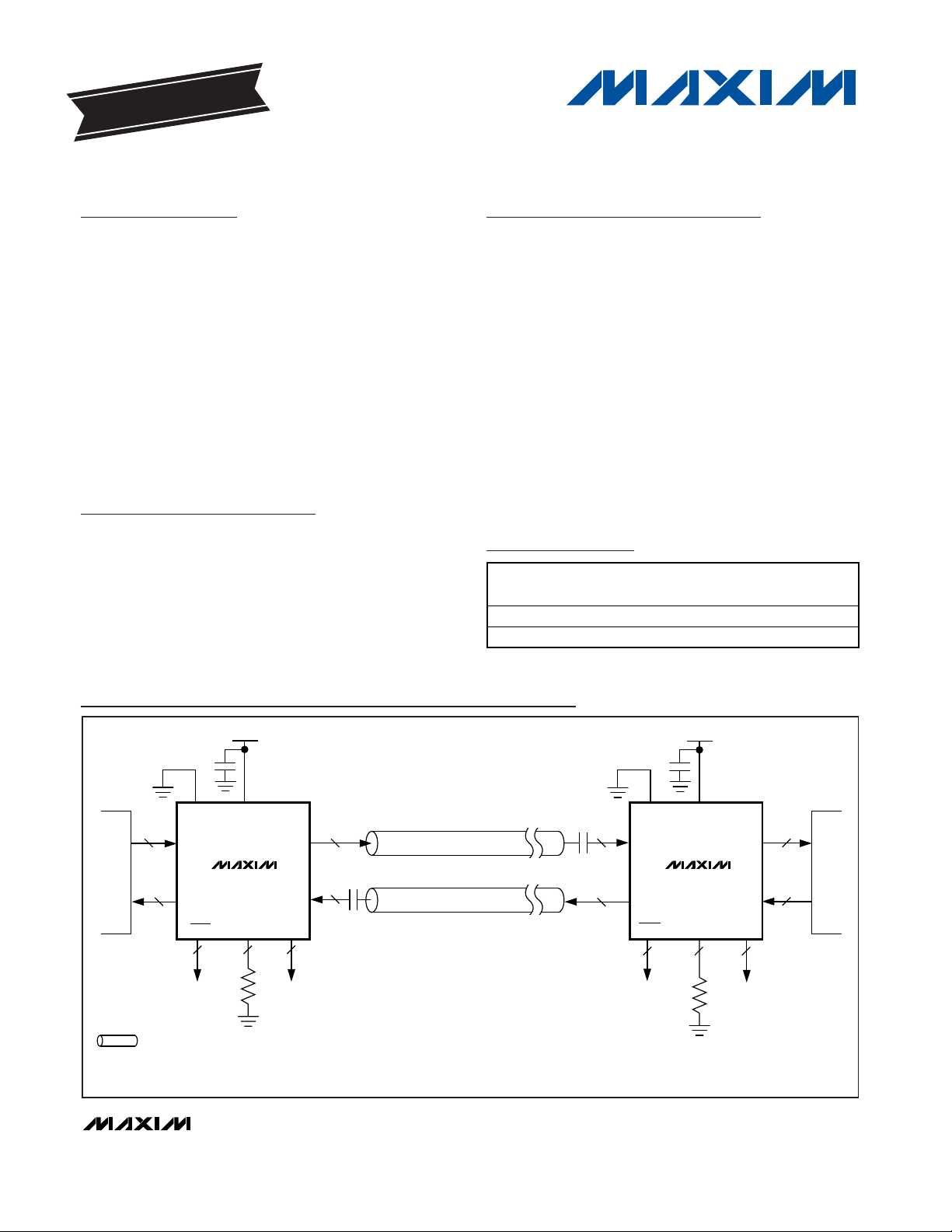
Typical Application Circuit
19-2289; Rev 2; 11/06
For pricing, delivery, and ordering information, please contact Maxim/Dallas Direct! at
1-888-629-4642, or visit Maxim’s website at www.maxim-ic.com.
Pin Configuration appears at end of data sheet.
+Denotes lead-free package.
EVALUATION KIT
AVAILABLE
PART
TEMP
RANGE
PIN-
PACKAGE
CODE
MAX3802UGK
68 QFN G6800-2
MAX3802UTK+
68 QFN T6800-4
DOUT_
EIN_
DIN_
EOUT_
MAX3802
DOUT_
EIN_
DIN_
THIS SYMBOL INDICATES A CONTROLLED-IMPEDANCE TRANSMISSION LINE.
EOUT_
RMOD_
CIM_
MAX3802
CARD 2
CARD 1
3.3V
LOS_
RMOD_
CIM_
LOS_
EP* V
CC
4
4
4
4
4
4
4 4 4
R
MOD_
COAX, TWIN-AX, OR PC BOARD x 4
COAX, TWIN-AX, OR PC BOARD x 4
*EP MUST BE SOLDERED TO GROUND FOR
PROPER THERMAL AND ELECTRICAL PERFORMANCE.
3.3V
EP* V
CC
R
MOD
_
4 4 4
4
4
PACKAGE
0°C to +85°C
0°C to +85°C
Page 2

MAX3802
3.2Gbps Quad Adaptive Cable Equalizer
with Cable Driver
2 _______________________________________________________________________________________
ABSOLUTE MAXIMUM RATINGS
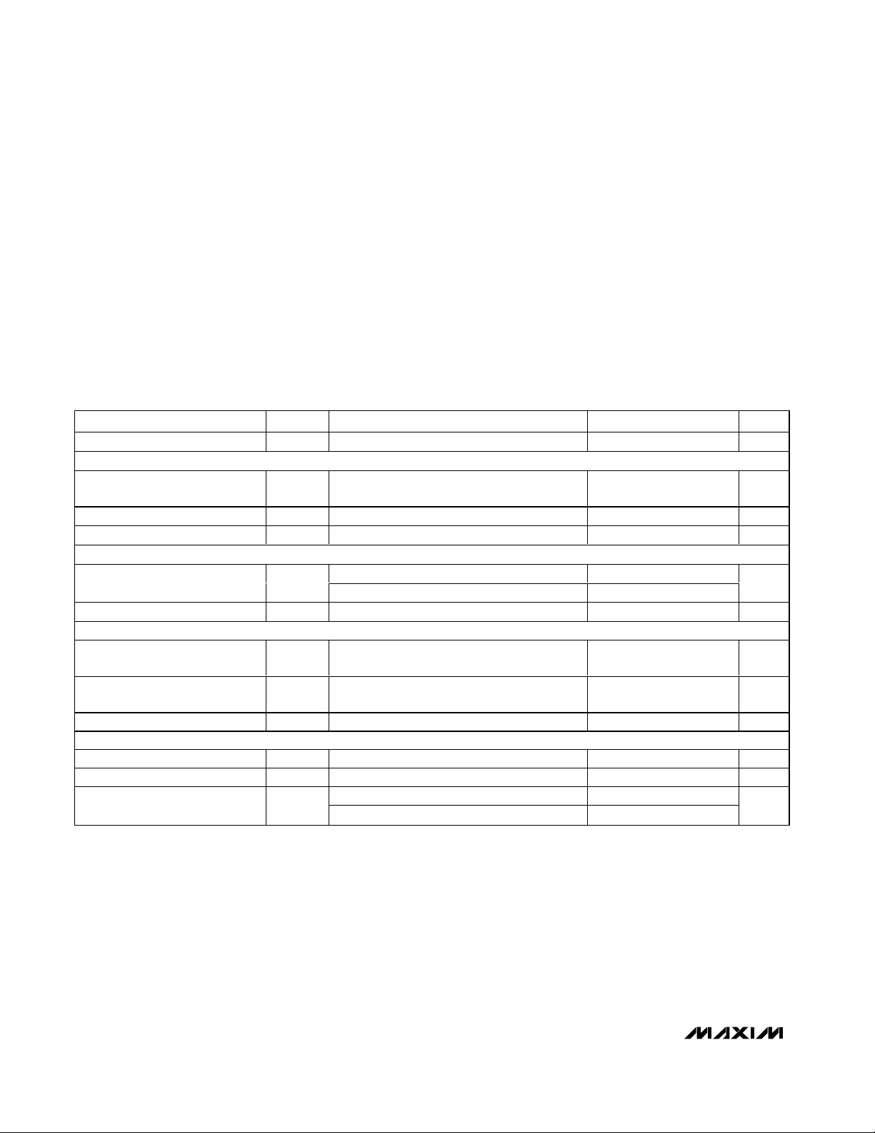
DC ELECTRICAL CHARACTERISTICS
(VCC= 3.14V to 3.46V, TA= 0°C to +85°C. Typical values are at VCC= 3.3V and TA= +25°C, unless otherwise noted.)
Stresses beyond those listed under “Absolute Maximum Ratings” may cause permanent damage to the device. These are stress ratings only, and functional
operation of the device at these or any other conditions beyond those indicated in the operational sections of the specifications is not implied. Exposure to
absolute maximum rating conditions for extended periods may affect device reliability.
Supply Voltage, VCC..............................................-0.5V to +6.0V
Voltage at LOS_, CIM_, and RMOD_ .........-0.5V to (V
CC
+ 0.5V)
Voltage at EIN_+, EIN_-,
DIN_+, and DIN_- ..........................(V
CC
- 1V) to (V
CC
+ 0.5V)
Current Out of EOUT_+, EOUT_-,
DOUT_+, and DOUT_- ...................................................25mA
Continuous Power Dissipation (T
A
= +85°C)
68-Pin QFN (derate 44.8mW/°C above +85°C) .............1.44W
Operating Ambient Temperature Range ................0°C to +85°C
Storage Ambient Temperature Range...............-55°C to +150°C
Lead Temperature (soldering, 10s) .................................+300°C
PARAMETER
CONDITIONS
UNITS
Supply Current I
CC
Includes external load current (Note 1)
mA
CABLE DRIVER INPUT SPECIFICATIONS
Input Voltage (Single Ended)
0.6
0.2
V
Input Voltage (Differential) V
DIN_
mV
P-P
Input Impedance Single ended 40 50 60 Ω
CABLE DRIVER OUTPUT SPECIFICATIONS
RMOD_ = 10kΩ (Note 2)
Output Voltage (Differential)
RMOD_ = 20kΩ (Note 2)
mV
P-P
Output Impedance Single ended 50
75 Ω
CABLE EQUALIZER INPUT SPECIFICATIONS
Minimum Cable Input
(Differential)
3.2Gbps, 30dB cable loss (Note 3)
mV
P-P
Maximum Cable Input
(Differential)
mV
P-P
Input Impedance 40 50 60 Ω
CABLE EQUALIZER OUTPUT SPECIFICATIONS
Output Voltage (Differential) (Note 2)
mV
P-P
Output Impedance Single ended 50
75 Ω
Output high (Note 4) 2.4
Voltage at LOS_
Output low (Note 4) 0.4
V
SYMBOL
V
+,
DIN_
V
-
DIN_
MIN TYP MAX
220 345
-
V
CC
400 1100
V
CC
+
750 825 1000
400 445 550
62.5
600
500 1000
62.5
400
Page 3

MAX3802
3.2Gbps Quad Adaptive Cable Equalizer
with Cable Driver
_______________________________________________________________________________________ 3
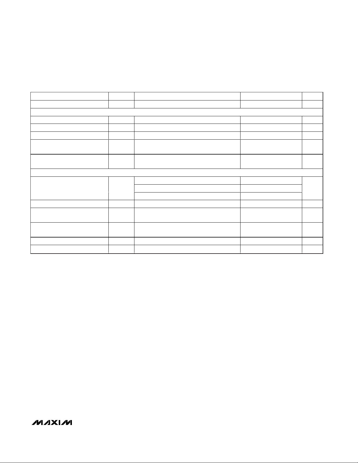
AC ELECTRICAL CHARACTERISTICS
(VCC= 3.14V to 3.46V, TA= 0°C to +85°C. Typical values are at VCC= 3.3V and TA= +25°C, unless otherwise noted.)
PARAMETER
SYMBOL
CONDITIONS
MIN
TYP
MAX
UNITS
Maximum Input Data Rate 3.2
Gbps
CABLE DRIVER SPECIFICATIONS
Random Jitter 3.2Gbps input 2.7 4
mUI
RMS
Deterministic Jitter (Notes 6, 9) 20 60
mUI
P-P
Output Edge Speed 20% to 80% 60 90 ps
Input Return Loss
(Differential)
≤ 2.5GHz -20 dB
Output Return Loss
(Differential)
≤ 2.5GHz -13 dB
EQUALIZER SPECIFICATIONS
0dB cable loss (Note 8)
24dB cable loss (Note 8)
Residual Jitter (Notes 7, 9)
30dB cable loss (Note 8)
UI
P-P
Output Edge Speed 20% to 80% 60 90 ps
Input Return Loss
(Differential)
≤ 2.5GHz -16 dB
Output Return Loss
(Differential)
≤ 2.5GHz -14 dB
Equalizer Compensation 1.6GHz (skin-effect losses only) 30 dB
Equalizer Time Constant (Note 10) 6 µs
Note 1: Equalizer total currents (equalizer with maximum equalization) and R
MOD
= 10kΩ (maximum driver swing).
Note 2: Input voltage within specification limits, 50Ω to V
CC
at each output.
Note 3: Minimum cable input for LOS_ to deassert high.
Note 4: 100kΩ load to ground. The minimum input signal level that turns off the LOS_ alarm depends on the data rate and cable length.
Note 5: AC electrical characteristics are guaranteed by design and characterization.
Note 6: V
DIN_
= 400mV
P-P
to 1100mV
P-P
(differential), 10kΩ≤R
MOD_
≤ 20kΩ, 3.2Gbps 213-1 PRBS plus 100 consecutive ones and
100 consecutive zeros.
Note 7: Includes random jitter and deterministic jitter for BER of 10
-12
.
Note 8: Differential cable input voltage = 400mV
P-P
, 3.2Gbps 213-1 PRBS plus 100 consecutive ones and 100 consecutive zeros.
Note 9: Isolation test: three channels driven with identical 3.2Gbps PRBS with maximum input signal to each equalizer and maxi-
mum input signal on driver. The measured channel meets the residual and random jitter specifications with an uncorrelated
3.2Gbps PRBS data at minimum input signal level on equalizer and maximum signal level on driver.
Note 10: Equalizer time constant measured from data on to closed-loop operation.
0.10 0.24
0.11 0.20
0.08 0.20
Page 4

MAX3802
3.2Gbps Quad Adaptive Cable Equalizer
with Cable Driver
4 _______________________________________________________________________________________
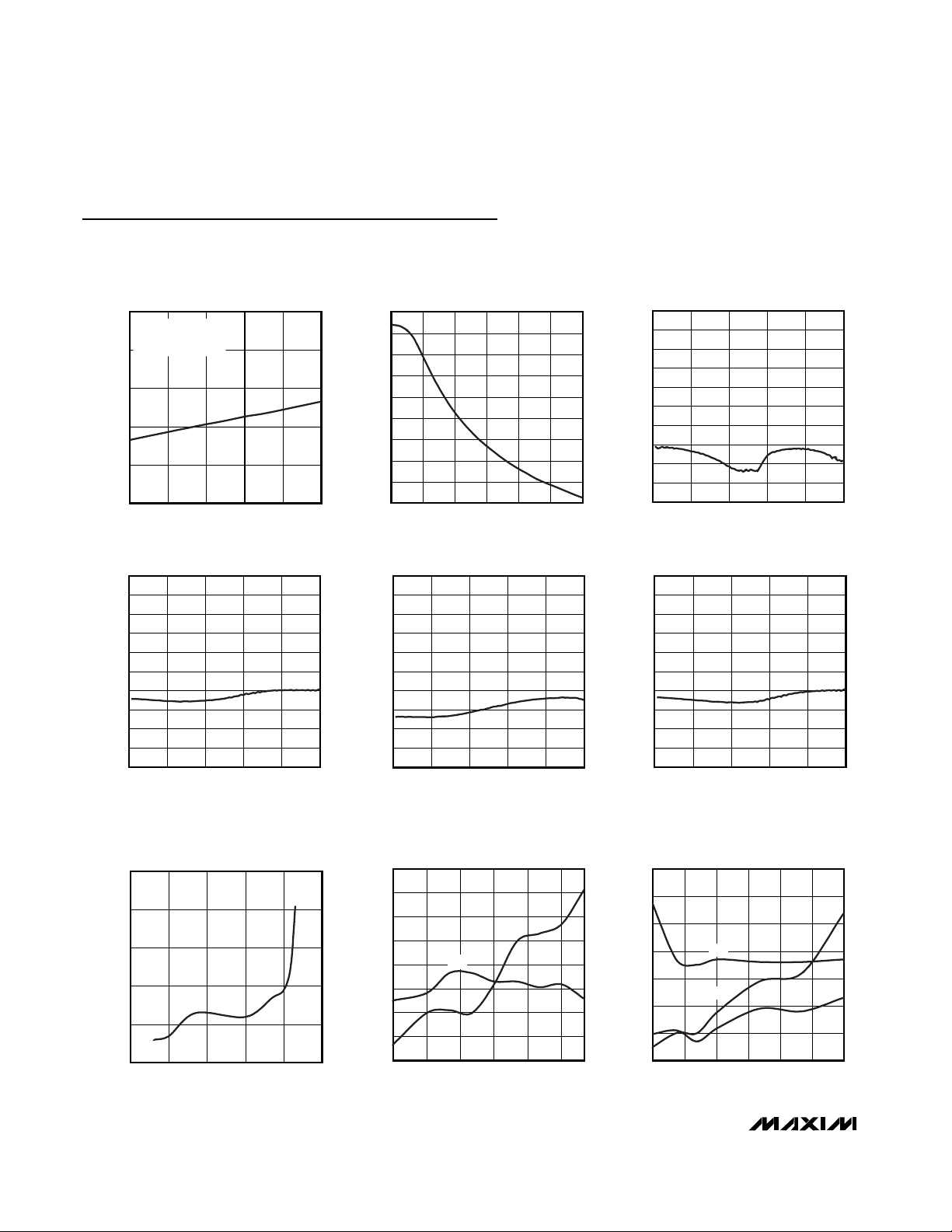
Typical Operating Characteristics
(VCC= 3.3V, TA= +25°C, all jitter measurements done at 3.2Gbps, 600mV cable input with 2
13
- 1 PRBS pattern with 100 consecutive ones and
100 consecutive zeros substituted. Note: Test pattern produces near-worst-case jitter results. Results vary with pattern, unless otherwise noted.)
150
180
240
210
270
300
-10 3010 50 70 90
SUPPLY CURRENT vs. TEMPERATURE
MAX3802 toc01
TEMPERATURE (°C)
SUPPLY CURRENT (mA)
RMOD = 15kΩ
ALL CHANNELS AT
MAX EQUALIZATION
400
600
500
900
800
700
1200
1100
1000
1300
4107 13161922
CABLE DRIVER OUTPUT vs. R
MOD
MAX3802 toc02
R
MOD
(kΩ)
DRIVER OUTPUT VOLTAGE (mV)
-50
-20
-30
-40
-10
0
10
20
30
40
50
01.60.8 2.4 3.2 4.0
DRIVER INPUT RETURN LOSS (S11)
MAX3802 toc03
FREQUENCY (GHz)
GAIN (dB)
-50
-20
-30
-40
-10
0
10
20
30
40
50
01.60.8 2.4 3.2 4.0
DRIVER OUTPUT RETURN LOSS (S22)
MAX3802 toc04
FREQUENCY (GHz)
GAIN (dB)
-50
-20
-30
-40
-10
0
10
20
30
40
50
01.60.8 2.4 3.2 4.0
EQUALIZER INPUT RETURN LOSS (S11)
MAX3802 toc05
FREQUENCY (GHz)
GAIN (dB)
-50
-20
-30
-40
-10
0
10
20
30
40
50
01.60.8 2.4 3.2 4.0
EQUALIZER OUTPUT RETURN LOSS (S22)
MAX3802 toc06
FREQUENCY (GHz)
GAIN (dB)
45
55
75
65
85
95
0.001 0.10.01 1 10 100
EQUALIZER RESIDUAL JITTER vs. POWER-SUPPLY
NOISE (100mV
P-P
SINE WAVE) (40ft OF TENSOLITE
TWIN-AX, 400mV
P-P
DIFFERENTIAL INPUT)
MAX3802 toc07
NOISE FREQUENCY (MHz)
JITTER (ps
P-P
)
45
55
65
75
85
95
105
115
125
150 450300 600 750 900
EQUALIZER RESIDUAL JITTER vs. CABLE
INPUT AMPLITUDE (RG179B 75Ω COAXIAL
CABLE, SINGLE ENDED)
MAX3802 toc08
CABLE INPUT AMPLITUDE (mV
P-P
)
JITTER (ps
P-P
)
25ft
72ft
35
55
45
75
65
95
85
105
300 600 750450 900 1050 1200
EQUALIZER RESIDUAL JITTER vs. CABLE
INPUT AMPLITUDE (TENSOLITE
TWIN-AX–DIFFERENTIAL)
MAX3802 toc09
CABLE DIFFERENTIAL INPUT AMPLITUDE (mV
P-P
)
JITTER (ps
P-P
)
70ft
10ft
40ft
Page 5

MAX3802
3.2Gbps Quad Adaptive Cable Equalizer
with Cable Driver
_______________________________________________________________________________________ 5
25
45
35
65
55
75
85
EQUALIZER RESIDUAL JITTER vs. CABLE
LENGTH (TENSOLITE TWIN-AX, 400mV
P-P
DIFFERENTIAL INPUT)
MAX3802 toc10
CABLE LENGTH (ft)
JITTER (ps
P-P
)
10 30 4020 50 60 70
3.2Gbps
2.5Gbps
622Mbps
40
50
70
60
80
90
25 4535 55 65
EQUALIZER RESIDUAL JITTER vs. CABLE
LENGTH (RG179B 75Ω COAXIAL, 300mV
P-P
SINGLE ENDED)
MAX3802 toc11
CABLE LENGTH (ft)
JITTER (ps
P-P
)
3.2Gbps
2.5Gbps
622Mbps
40
60
50
80
70
90
100
40 90
EQUALIZER RESIDUAL JITTER vs. LINE
LENGTH (FR-4 6mil STRIPLINE, 300mV
P-P
SINGLE ENDED)
MAX3802 toc12
LINE LENGTH (in)
JITTER (ps
P-P
)
6050 70 80
3.2Gbps
2.5Gbps
622Mbps
0
0.10
0.05
0.20
0.15
0.25
0.30
CIM VOLTAGE vs. CABLE LENGTH (TENSOLITE
TWIN-AX, 400mV
P-P
DIFFERENTIAL)
MAX3802 toc13
CABLE LENGTH (ft)
CIM VOLTAGE (V
CC
- V
CIM
) (V)
10 30 4020 50 60 70
EQUALIZER INPUT AFTER 115ft OF
CABLE (TOP) EQUALIZER OUTPUT (BOTTOM)
MAX3802 toc14
48ps/div (3.2Gbps)
EQUALIZER OUTPUT EYE DIAGRAM AFTER
155ft OF 50Ω GORE-89 CABLE (400mV
P-P
)
MAX3802 toc15
60ps/div (2.5Gbps)
CABLE OUTPUT EYE DIAGRAM AFTER 70ft
OF TENSOLITE TWIN-AX CABLE (2
7
- 1 PRBS
NO EQUALIZATION)
MAX3802 toc16
60ps/div (2.5Gbps)
EQUALIZER OUTPUT EYE DIAGRAM AFTER 70ft
OF TENSOLITE TWIN-AX CABLE (2
7
- 1 PRBS)
MAX3802 toc17
48ps/div (3.2Gbps)
EQUALIZER OUTPUT EYE DIAGRAM AFTER 72ft
OF 75Ω RG179 CABLE
(300mV
P-P
SINGLE ENDED, 223 - 1 PRBS)
MAX3802 toc18
Typical Operating Characteristics (continued)
(VCC= 3.3V, TA= +25°C, all jitter measurements done at 3.2Gbps, 600mV cable input with 2
13
- 1 PRBS pattern with 100 consecutive ones and
100 consecutive zeros substituted. Note: Test pattern produces near-worst-case jitter results. Results vary with pattern, unless otherwise noted.)
Page 6

MAX3802
3.2Gbps Quad Adaptive Cable Equalizer
with Cable Driver
6 _______________________________________________________________________________________
60ps/div (2.5Gbps)
EQUALIZER OUTPUT EYE DIAGRAM AFTER 60in OF
FR-4 6mil STRIPLINE (DIFFERENTIAL, 2
7
- 1 PRBS)
MAX3802 toc19
60ps/div (2.5Gbps)
EQUALIZER OUTPUT EYE DIAGRAM AFTER 288ft
OF RG59 CABLE (300mV
P-P
SINGLE ENDED,
2
23
- 1 PRBS)
MAX3802 toc20
60ps/div (2.5Gbps)
EQUALIZER OUTPUT EYE DIAGRAM AFTER 50ft
OF MADISON 14887 SHIELDED TWISTED-PAIR
CABLE (2
7
- 1 PRBS)
MAX3802 toc21
Typical Operating Characteristics (continued)
(VCC= 3.3V, TA= +25°C, all jitter measurements done at 3.2Gbps, 600mV cable input with 2
13
- 1 PRBS pattern with 100 consecutive ones and
100 consecutive zeros substituted. Note: Test pattern produces near-worst-case jitter results. Results vary with pattern, unless otherwise noted.)
Pin Description
PIN NAME FUNCTION
1, 4, 6, 9 V
CCE
1 3.3V Supply Voltage for Equalizer 1
2 EIN1- Negative Equalizer 1 Input, CML
3 EIN1+ Positive Equalizer 1 Input, CML
5 CIM1 Cable Integrity Monitor 1 Output
7 EOUT1- Negative Equalizer 1 Output, CML
8 EOUT1+ Positive Equalizer 1 Output, CML
10 RMOD1 Driver 1 Output Modulation Adjust
11, 14 V
CCD
1 3.3V Supply Voltage for Driver 1
12 DOUT1- Negative Driver 1 Output, CML
13 DOUT1+ Positive Driver 1 Output, CML
15 DIN1- Negative Driver 1 Input, CML
16 DIN1+ Positive Driver 1 Input, CML
17 LOS1 Equalizer 1 Loss-of-Signal, TTL, Active Low
V
CCE
2 3.3V Supply Voltage for Equalizer 2
19 EIN2- Negative Equalizer 2 Input, CML
20 EIN2+ Positive Equalizer 2 Input, CML
22 CIM2 Cable Integrity Monitor 2 Output
24 EOUT2- Negative Equalizer 2 Output, CML
25 EOUT2+ Positive Equalizer 2 Output, CML
27 RMOD2 Driver 2 Output Modulation Adjust
28, 31 V
CCD
2 3.3V Supply Voltage for Driver 2
29 DOUT2- Negative Driver 2 Output, CML
30 DOUT2+ Positive Driver 2 Output, CML
18, 21, 23, 26
Page 7

MAX3802
3.2Gbps Quad Adaptive Cable Equalizer
with Cable Driver
_______________________________________________________________________________________ 7
Pin Description (continued)
PIN NAME FUNCTION
32 DIN2- Negative Driver 2 Input, CML
33 DIN2+ Positive Driver 2 Input, CML
34 LOS2 Equalizer 2 Loss-of-Signal, TTL, Active Low
35, 38, 40, 43
V
CCE
3 3.3V Supply Voltage for Equalizer 3
36 EIN3- Negative Equalizer 3 Input, CML
37 EIN3+ Positive Equalizer 3 Input, CML
39 CIM3 Cable Integrity Monitor 3 Output
41 EOUT3- Negative Equalizer 3 Output, CML
42 EOUT3+ Positive Equalizer 3 Output, CML
44 RMOD3 Driver 3 Output Modulation Adjust
45, 48 V
CCD
3 3.3V Supply Voltage for Driver 3
46 DOUT3- Negative Driver 3 Output, CML
47 DOUT3+ Positive Driver 3 Output, CML
49 DIN3- Negative Driver 3 Input, CML
50 DIN3+ Positive Driver 3 Input, CML
51 LOS3 Equalizer 3 Loss-of-Signal, TTL, Active Low
52, 55, 57, 60
V
CCE
4 3.3V Supply Voltage for Equalizer 4
53 EIN4- Negative Equalizer 4 Input, CML
54 EIN4+ Positive Equalizer 4 Input, CML
56 CIM4 Cable Integrity Monitor 4 Output
58 EOUT4- Negative Equalizer 4 Output, CML
59 EOUT4+ Positive Equalizer 4 Output, CML
61 RMOD4 Driver 4 Output Modulation Adjust
62, 65 V
CCD
4 3.3V Supply Voltage for Driver 4
63 DOUT4- Negative Driver 4 Output, CML
64 DOUT4+ Positive Driver 4 Output, CML
66 DIN4- Negative Driver 4 Input, CML
67 DIN4+ Positive Driver 4 Input, CML
68 LOS4 Equalizer 4 Loss-of-Signal, TTL, Active Low
EP
Exposed
Pad
Ground. Must be soldered to the circuit board ground for proper thermal and electrical
performance (see EP Package).
Page 8

MAX3802
Detailed Description
The MAX3802 has four independent adaptive equalizers (receivers) and four independent drivers. Disconnecting the power pins of unused equalizers and
drivers lowers the power consumption of the MAX3802.
Equalizer and driver descriptions apply to the four identical sections.
Cable Driver
The cable driver accepts differential or single-ended
CML input data at rates up to 3.2Gbps. The maximum
CML output of the driver can be adjusted over a typical
range of 445mV to 825mV by changing the value of the
R
MOD_
resistor between 10kΩ and 20kΩ (resistor con-
nected between RMOD_ pin and ground).
Adaptive Cable Equalizer
The adaptive cable equalizer is capable of equalizing
differential or single-ended CML input data at rates up
to 3.2Gbps. It automatically adjusts to attenuation levels of 30dB at 1.6GHz (due to skin-effect losses in copper cable). The equalizer consists of a CML input
buffer, a flat-response amplifier, a skin-effect compensation amplifier, a current-steering network, a dual
power-detector feedback loop, an output limiting amplifier, and a CML output buffer (Figure 1).
General Theory of Operation
The shape of the power spectrum of a random bit
stream can be described by the square of the wellknown sinc function, where sinc(f) = sin(πf)/(πf) for f ≠ 0.
For sufficiently long bit patterns (nonrandom bit
stream), sinc
2
(f) is a good approximation. From the
shape of the sinc2(f) function, the ratio of the power
densities at any two frequencies can be estimated. The
MAX3802 adaptive equalizer employs this principle by
incorporating a feedback loop that continuously monitors the power at high- and low-frequency bands and
3.2Gbps Quad Adaptive Cable Equalizer
with Cable Driver
8 _______________________________________________________________________________________
MAX3802
VARIABLE
ATTENUATOR
VARIABLE
ATTENUATOR
CURRENT-STEERING NETWORK
Σ
FLAT
RESPONSE
AMP
CML
CML
CML CML
SKINEFFECT
COMP
AMP
|H(f)|
POWER
DETECTOR
EIN_
DOUT_
2
2
LOS_
CABLE
DRIVER
|H(f)|
√
f
RMOD_
R
MOD_
2
DIN_
2
EOUT_
LIMITING
AMP
600MHz
PWR DETECTOR
200MHz
PWR DETECTOR
LOOP
FILTER
Figure 1. MAX3802 Functional Diagram
Page 9

dynamically adjusts the equalizer to maintain the correct power ratio.
CML Input and Output Buffers
The input and output buffers are implemented using
CML. Equivalent circuits are shown in Figures 2 and 3.
For details on interfacing with CML, refer to Maxim
Application Note HFAN-01.0, Interfacing Between CML,
PECL, and LVDS.
Flat-Response and Skin-Effect
Compensation Amplifiers
The buffered input waveform is fed equally to two
amplifiers—the flat-response amplifier and the skineffect compensation amplifier. The flat-response amplifier has a constant gain over the entire frequency range
of the device, and the skin-effect compensation amplifier has a gain characteristic that approximates the
inverse of the skin-effect attenuation in copper cable.
The skin-effect attenuation, in dB per unit length, is proportional to the square root of the frequency. The output currents from the amplifiers are supplied to the
current-steering network.
Current-Steering Network
The function of the current-steering network is to combine adjustable quantities of the output currents from
the flat-response and skin-effect compensation amplifiers in order to achieve a desired current ratio. The
ratio adjustment is controlled by the dual power-detector feedback loop.
The current-steering network is implemented with a pair
of variable attenuators that feed into a current-summing
node. The variable attenuators are used to attenuate
the output currents of the flat-response and skin-effect
compensation amplifiers under control of the dual
power-detector feedback loop. The outputs of the two
attenuators are combined at the summing node and
then fed to the output-limiting amplifier and the feedback loop.
Dual Power-Detector Feedback Loop
The outputs of the current-steering network are applied
to the inputs of 200MHz and 600MHz power detectors.
The outputs of the power detectors are applied to the
loop-filter amplifier. This amplifier controls the variable
attenuators in the current-steering network.
Output Limiting Amplifier
The output limiting amplifier amplifies the signal from
the current-steering network to achieve the specified
output voltage swing.
Applications Information
Refer to Maxim Application Note HFDN-10.0,
Equalizing Gigabit Copper Cable Links with the
MAX3800 (available at www.maxim-ic.com) for addi-
tional application information.
Selecting R
MOD
The cable driver output amplitude can be adjusted by
connecting a resistor (R
MOD
) with a value from 10kΩ to
20kΩ between the RMOD_ pin and ground. The exact
output amplitude of the driver is dependent on several
MAX3802
3.2Gbps Quad Adaptive Cable Equalizer
with Cable Driver
_______________________________________________________________________________________ 9
_IN_-
_IN_+
ESD
STRUCTURES
V
CC
50Ω
50Ω
MAX3802
Figure 2. CML Input Structure
ESD
STRUCTURES
62.5Ω 62.5Ω
_OUT_-
_OUT_+
V
CC
MAX3802
Figure 3. CML Output Structure
Page 10

MAX3802
factors. See the Typical Operating Characteristics Cable
Driver Output Voltage vs. R
MOD
for typical values.
Cable Integrity Monitor
The CIM_ output voltage is directly proportional to the
output current of the loop amplifier (which controls the
current-steering network; see Detailed Description).
This is an analog voltage output that indicates the
amount of equalization being applied.
The amount of equalization (and thus the CIM_ output
level) is affected by cable type, cable length, signal
bandwidth, etc. See the Typical Operating Char-
acteristics CIM Voltage vs. Cable Length for typical values under specific conditions.
Loss-of-Signal (
LOS_
) Output
Loss of signal is indicated by the LOS_ output. A low
level on LOS_ indicates that the equalizer input power
has dropped below a threshold. When there is sufficient input voltage to the channel (typically greater than
250mV), LOS_ is high. The LOS_ output is suitable for
indicating problems with the transmission link caused
by, for example, a broken cable or a defective driver.
Data Spectrum for Equalizer
The MAX3802 equalizer design requires the data
stream be scrambled or coded to provide a rich frequency spectrum for the adaptation algorithm.
Scrambled patterns or coded patterns with scrambled
content, such as 64b/66b or SONET PRBS, are ideal.
Some coded patterns, such as 8b/10b, lack low-frequency energy and can be nonoptimal, requiring the
user to characterize the specific application. In the
absence of an input signal (nonstandard application),
amplified noise may appear at the output due to the
large gain of the device.
Single-Ended Operation
For single-ended operation of the cable driver or equalizer, connect the unused input to ground through a
series combination of a capacitor (of equal value to
other AC-coupling capacitors) and a 50Ω resistor. Note
that the MAX3802 is specified for differential operation.
Layout Considerations
The MAX3802’s performance can be significantly
affected by circuit board layout and design. Use good
high-frequency design techniques, including minimizing ground inductance and using controlled-impedance transmission lines for the high-frequency data
signals. Power-supply decoupling capacitors should be
placed as close as possible to VCC.
Exposed-Pad Package
The EP on the 68-pin QFN provides a very low thermal
resistance path for heat removal from the IC. The pad is
the electrical ground on the MAX3802 and must be soldered to the circuit board ground for proper thermal and
electrical performance. Refer to Maxim Application Note
HFAN-08.1, Thermal Considerations for QFN and Other
Exposed-Pad Packages (available at www.maximic.com) for additional application information.
Chip Information
TRANSISTOR COUNT: 5408
PROCESS: Bipolar (silicon germanium)
3.2Gbps Quad Adaptive Cable Equalizer
with Cable Driver
10 ______________________________________________________________________________________
MAX3802
V
CCD
1
RMOD1
V
CCE
1
EOUT1+
EOUT1-
V
CCE
1
DIN1+
DIN1-
V
CCD
1
DOUT1+
DOUT1-
CIM1
V
CCE
1
EIN1+
EIN1-
V
CCE
1
11
10
9
8
7
6
5
4
3
2
16
15
14
13
12
1
17LOS1
EIN2-
QFN*
V
CCE
2
V
CCE
2
EIN2+
V
CCE
2
CIM2
EOUT2+
EOUT2-
RMOD2
V
CCE
2
DOUT2-
V
CCD
2
V
CCD
2
DOUT2+
DIN2-
2322212019 2726252418 2928 323130
DIN2+
3433
*THE EXPOSED PAD OF THE QFN PACKAGE MUST BE SOLDERED TO GROUND
FOR PROPER THERMAL AND ELECTRICAL OPERATION OF THE MAX3802.
LOS2
38
39
40
41
42
43
44
45
46
47
DOUT3+
DOUT3-
V
CCD
3
RMOD3
V
CCE
3
EOUT3+
EOUT3-
V
CCE
3
CIM3
V
CCE
3
35
36
37
EIN3+
EIN3-
V
CCE
3
48 V
CCD
3
49
50
DIN3+
DIN3-
51 LOS3
5859606162 5455565763
DOUT4-
TOP VIEW
V
CCD
4
RMOD4
V
CCE
4
EOUT4+
EOUT4-
V
CCE
4
CIM4
V
CCE
4
EIN4+
5253
EIN4-
V
CCE
4
64
DOUT4+
656667
DIN4+
DIN4-
V
CCD
4
68
LOS4
Pin Configuration
Page 11

MAX3802
3.2Gbps Quad Adaptive Cable Equalizer
with Cable Driver
______________________________________________________________________________________ 11
68L QFN.EPS
C
1
2
21-0122
PACKAGE OUTLINE, 68L QFN, 10x10x0.9 MM
Package Information
(The package drawing(s) in this data sheet may not reflect the most current specifications. For the latest package outline information
go to www.maxim-ic.com/packages
.)
Page 12

MAX3802
3.2Gbps Quad Adaptive Cable Equalizer
with Cable Driver
Maxim cannot assume responsibility for use of any circuitry other than circuitry entirely embodied in a Maxim product. No circuit patent licenses are
implied. Maxim reserves the right to change the circuitry and specifications without notice at any time.
12 ____________________Maxim Integrated Products, 120 San Gabriel Drive, Sunnyvale, CA 94086 408-737-7600
© 2006 Maxim Integrated Products is a registered trademark of Maxim Integrated Products.
C
1
2
21-0122
PACKAGE OUTLINE, 68L QFN, 10x10x0.9 MM
Package Information (continued)
(The package drawing(s) in this data sheet may not reflect the most current specifications. For the latest package outline information
go to www.maxim-ic.com/packages
.)
Revision History
Rev 0; 1/02: Initial data sheet release.
Rev 1; 5/03: Added package code to Ordering Information table (page 1); updated package outline
(pages 11–12).
Rev 2; 11/06: Added lead-free package to Ordering Information table (page 1).
 Loading...