Page 1
General Description
The MAX3787 is a 1Gbps to 12.5Gbps equalization
network that compensates for transmission medium losses encountered with FR4 and cables. The equalization
network is composed entirely of passive components
and functions equally well for 8b/10b or scrambled signals. It is packaged in a small 1.5mm x 1.5mm chipscale package (UCSP™) that can be placed anywhere
along the transmission medium to increase jitter margin
for high-speed interconnects. Roughly the size of two
0603 components, the MAX3787 easily provides placement and routing flexibility.
At 8.5Gbps, the MAX3787 compensates for spans up to
18in of FR4 and 7m of cable. At 12.5Gbps, the MAX3787
compensates for spans up to 12in of FR4 and 3m of
cable. Input and output impedance is 100Ω differential.
The MAX3787 requires no power and operates over a
-40°C to +125°C temperature range.
Applications
Backplane Interconnect Compensation
Cable Interconnect Compensation
Chip-to-Chip Link Extensions
Ethernet and Fibre-Channel Serial Modules
Chassis Life Extension
Features
♦ No Power Supply Required
♦ Small 1.5mm x 1.5mm Chip-Scale Package
♦ Passive Equalization Reduces ISI
♦ Operates from 1Gbps to 12.5Gbps
♦ Extends Board Link
♦ Extends Cable Link
♦ Coding Independent, 8b/10b or Scrambled
MAX3787
1Gbps to 12.5Gbps
Passive Equalizer for Backplanes and Cables
________________________________________________________________
Maxim Integrated Products
1
19-0406; Rev 2; 2/08
EVALUATION KIT
AVAILABLE
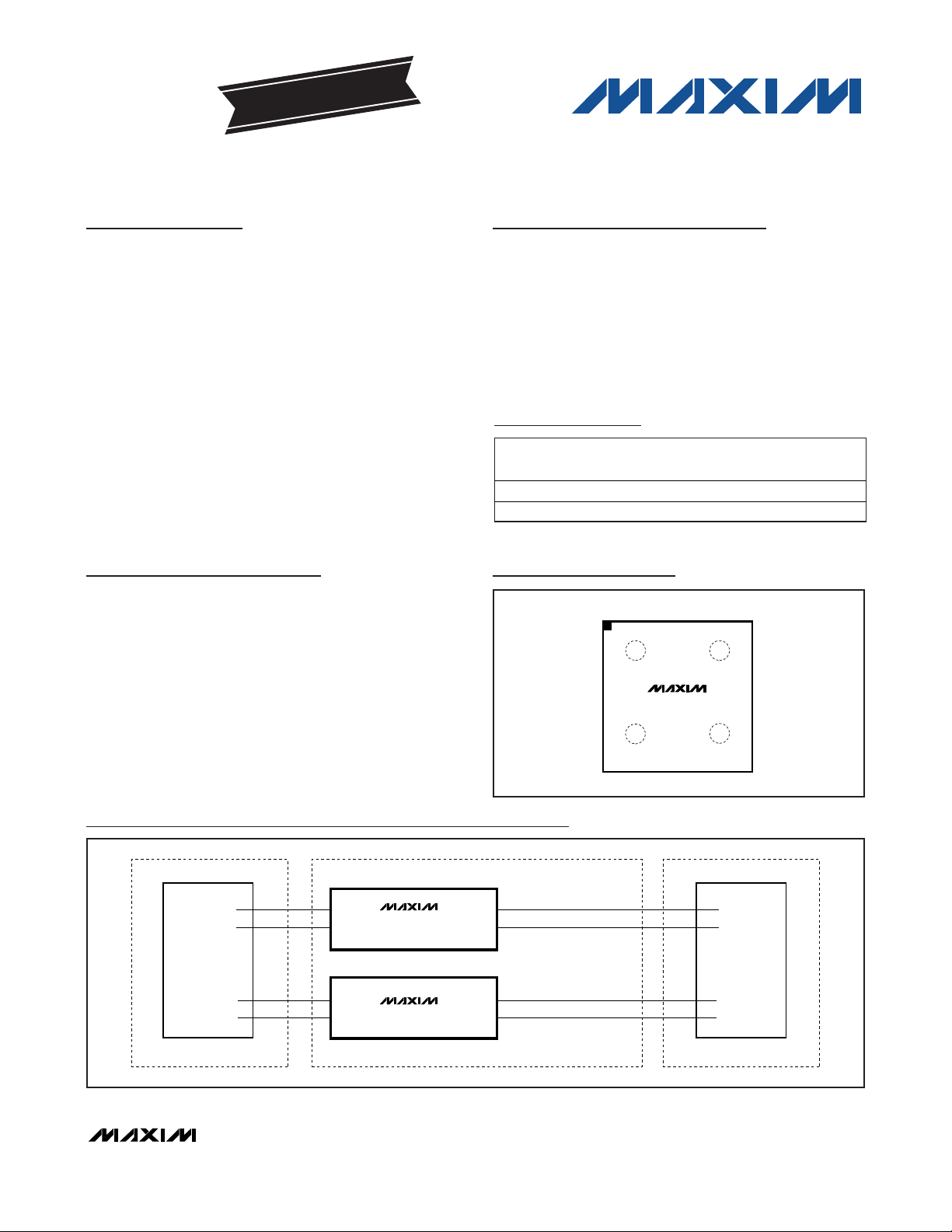
Pin Configuration
Ordering Information
UCSP is a trademark of Maxim Integrated Products, Inc.
Typical Application Circuits continued at end of data sheet.
Typical Application Circuits
+
Denotes a lead-free package.
For pricing, delivery, and ordering information, please contact Maxim Direct at 1-888-629-4642,
or visit Maxim’s website at www.maxim-ic.com.
PART TEMP RANGE
MAX3787ABL -40°C to +125°C 4 UCSP B9-7
MAX3787AWL+ -40°C to +125°C 4 WLP W91B1+3
PINPACKAGE
PKG
CODE
TOP VIEW
A
B
21
3
IN+
MAX3787
OUT+
C
IN- OUT-
UCSP/WLP
LINE CARD
Tx(100Ω) (100Ω)
(100Ω)
Rx
IN- OUT-
OUT- IN-
ALL PASSIVE BACKPLANE INTERCONNECT
OUT+IN+
MAX3787
IN+OUT+
MAX3787
100Ω FR4
100Ω FR4
SWITCH CARD
Rx
(100Ω)
Tx
Page 2

MAX3787
2 _______________________________________________________________________________________
ELECTRICAL CHARACTERISTICS
(Specifications guaranteed over specified operating conditions. Typical values measured at TA = +25°C.)
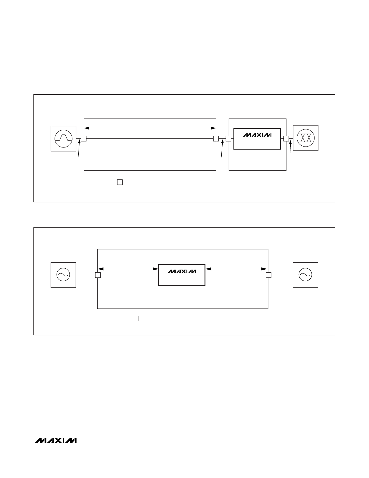
Note 1: Signal applied differentially at point A as shown in Figure 1. The deterministic jitter at point B is from media-induced loss,
not from clock-source modulation. Deterministic jitter is measured at the 50% vertical level of the signal at point C.
Note 2: Difference in deterministic jitter between reference points A and C in Figure 1. Stress pattern: 2
7
PRBS, 100 zeros, 1, 0, 1, 0,
27 PRBS, 100 ones, 0, 1, 0, 1.
1Gbps to 12.5Gbps
Passive Equalizer for Backplanes and Cables
ABSOLUTE MAXIMUM RATINGS
Stresses beyond those listed under “Absolute Maximum Ratings” may cause permanent damage to the device. These are stress ratings only, and functional
operation of the device at these or any other conditions beyond those indicated in the operational sections of the specifications is not implied. Exposure to
absolute maximum rating conditions for extended periods may affect device reliability.
Voltage between (IN+ and OUT+) or (IN- and OUT-) ..............+2V
Voltage between (IN+ and IN-) or (OUT+ and OUT-) ..............+4V
Voltage between (IN+ and OUT-) or (IN- and OUT+) ..............+4V
Continuous Power Dissipation (T
A
= +70°C)
4-Bump UCSP (derate 3.0mW/°C above +70°C).........238mW
Operating Junction Temperature........................................+150°C
Storage Ambient Temperature Range .................-55°C to +150°C
OPERATING CONDITIONS
Operating Ambient Temperature
Bit Rate NRZ data 1 12.5 Gbps
CID Tolerance Consecutive identical digits 100 Bits
Supply Current 0.0 mA
PARAMETER SYM B O L CONDITIONS MIN TYP MAX UNITS
T
A
PARAMETER SYM B O L CONDITIONS MIN TYP MAX UNITS
-40 +25 +125 °C
Input Swing Measured differentially at point A in Figure 1 3600 mV
Compensation 5GHz relative to 100MHz 6 dB
Input Impedance Differential, Z
Output Impedance Differential, Z
Through Response Relative to ideal load, see Figure 2 for setup See Figure 3 for limits
Input Return Loss 100MHz to 6GHz 15 dB
Output Return Loss 100MHz to 6GHz 15 dB
Resistance IN+ to IN- and OUT+
to OUT-
Resistance IN+ to OUT+ and
IN- to OUT-
Resistance IN+ to OUT- and
IN- to OUT+
DC Gain (OUT/IN) Z
Residual Deterministic Jitter
(Table 1, Notes 1, 2)
No load, high impedance on all ports 112 152 Ω
No load, high impedance on all ports 32 44 Ω
No load, high impedance on all ports 112 152 Ω
= 100Ω 0.5
LOAD
3.125Gbps and 6.25Gbps, 18in of 6mil
microstrip FR4
8.5Gbps, 10.0Gbps, and 12.5Gbps,
18in of 6mil microstrip FR4
= 100Ω 100 Ω
LOAD
= 100Ω 100 Ω
SOURCE
0.05
0.10
P-P
UI
Page 3
MAX3787
Figure 1. Residual Deterministic Jitter Test Circuit
Figure 2. Frequency Response Test Circuit Using Vector Network Analyzer (VNA)
1Gbps to 12.5Gbps
Passive Equalizer for Backplanes and Cables
_______________________________________________________________________________________ 3
FR4 TEST BOARD
SIGNAL SOURCE
A
VNA SOURCE
1in DUAL 50Ω
MICROSTRIP LINE
0in ≤ L ≤ 18in
SEE TABLE 1 FOR PCB PARAMETERS.
REPRESENTS EDGE-MOUNTED SMA CONNECTOR.
ROGERS 4350 BOARD
MAX3787
B
1in DUAL 50Ω
MICROSTRIP LINE
ROGERS 4350 BOARD
OSCILLOSCOPE
MAX3787
C
VNA DETECTOR
REPRESENTS EDGE-MOUNTED SMA CONNECTOR.
Page 4
MAX3787
4 _______________________________________________________________________________________
1Gbps to 12.5Gbps
Passive Equalizer for Backplanes and Cables
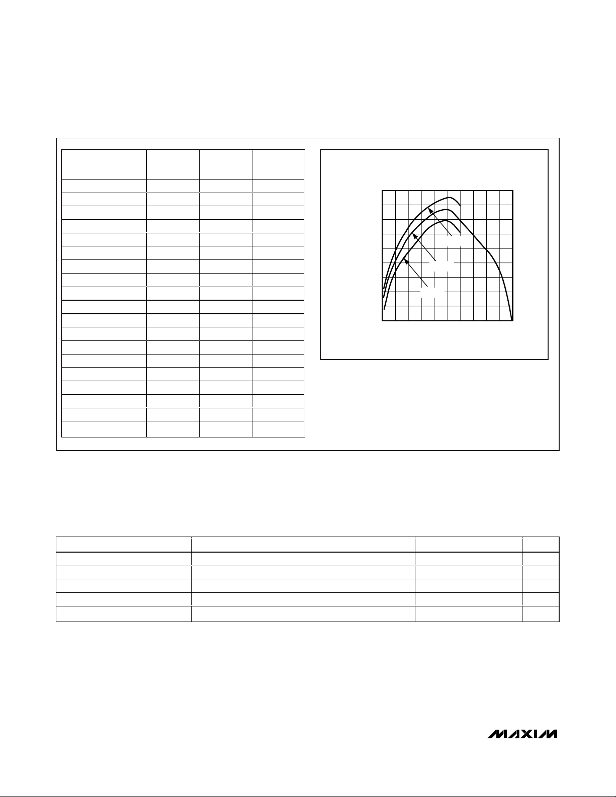
Figure 3. Through Response Limits
Table 1. PCB Assumptions (Board Material is FR4)
FREQUENCY
100MHz -8.2 -7.4 -6.8
200MHz -7.9 -7.0 -6.4
300MHz -7.5 -6.6 -6.0
500MHz -6.8 -6.0 -5.3
1.0GHz -5.5 -4.8 -4.2
2.0GHz -4.2 -3.2 -2.5
3.0GHz -3.1 -2.2 -1.5
4.0GHz -2.3 -1.5 -0.8
5.0GHz -2.1 -1.3 -0.5
5.5GHz -2.4 -1.6 -0.6
6.0GHz -2.9 -2.1 -1.1
6.5GHz — -2.6 —
7.0GHz — -3.1 —
7.5GHz — -3.6 —
8.0GHz — -4.1 —
8.5GHz — -4.7 —
9.0GHz — -5.5 —
9.5GHz — -7.0 —
10.0GHz — -9.0 —
MIN
(dB)
TYP
(dB)
MAX
(dB)
THROUGH-RESPONSE LIMITS
(RELATIVE TO IDEAL LOAD)
0
-1
-2
-3
-4
S21 (dB)
-5
-6
-7
-8
-9
010
MAX
TYP
MIN
986723451
FREQUENCY (GHz)
PARAMETER CONDITIONS MIN TYP MAX UNITS
Transmission Line Edge-coupled microstrip line 6 mil
Relative Permittivity at 1GHz FR4 or similar 4.0 —
Loss Tangent FR4 or similar 0.02 —
Metal Thickness 1oz copper 1.4 mil
Impedance Differential 90 100 110 Ω
Page 5
MAX3787
1Gbps to 12.5Gbps
Passive Equalizer for Backplanes and Cables
_______________________________________________________________________________________
5
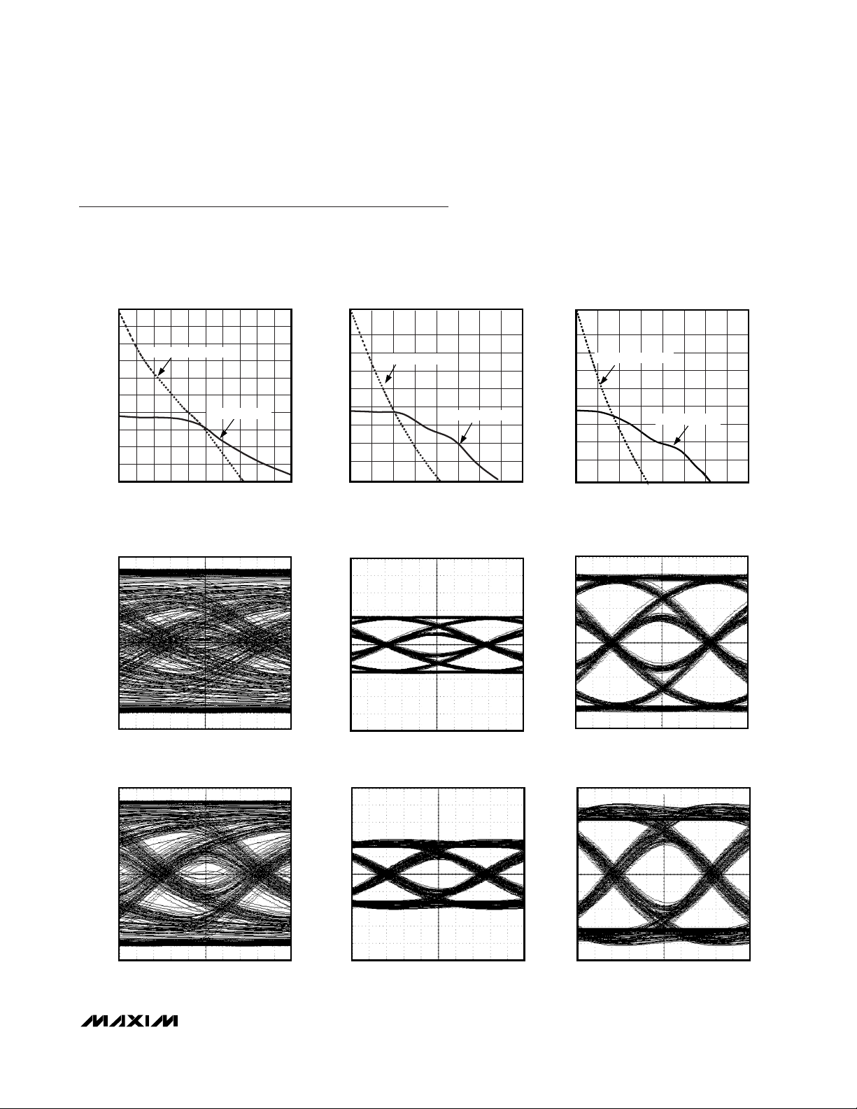
Typical Operating Characteristics
(TA= +25°C, unless otherwise noted. All measurements were done with 1V
P-P
at the source. Stress pattern: 27PRBS, 100 zeros, 1, 0, 1,
0, 2
7
PRBS, 100 ones, 0, 1, 0, 1. Residual deterministic jitter graphs were measured using Tektronix’s FrameScan®. Deterministic jitter of
the system was subtracted from the measured value. Eye diagrams acquired by FrameScan include deterministic jitter of the system
(approximately 9ps) but not random jitter. Twin-ax cable: Amphenol Spectra-Strip
®
Skewclear®100Ω 24AWG.)
FrameScan is a registered trademark of Tektronix.
Spectra-Strip and Skewclear are registered trademarks of Amphenol.
VERTICAL EYE OPENING vs. LENGTH
(4.25Gbps, STRESS PATTERN)
1000
900
)
800
P-P
700
600
500
400
300
VERTICAL EYE OPENING (mV
200
100
WITHOUT EQUALIZER
WITH EQUALIZER
0
01015205 253035 4540 50
FR4 BOARD LENGTH (in)
EYE DIAGRAM OF UNEQUALIZED SIGNAL
(18in FR4, 12.5Gbps, STRESS PATTERN)
MAX3787toc01
MAX3787toc04
VERTICAL EYE OPENING vs. LENGTH
(8.5Gbps, STRESS PATTERN)
900
800
)
P-P
700
600
500
400
300
200
VERTICAL EYE OPENING (mV
100
0
WITHOUT EQUALIZER
01015205 25303540
FR4 BOARD LENGTH (in)
EYE DIAGRAM OF EQUALIZED SIGNAL
(18in FR4, 12.5Gbps, STRESS PATTERN)
VERTICAL EYE OPENING vs. LENGTH
(10.3125Gbps, STRESS PATTERN)
900
800
)
MAX3787toc02
P-P
WITH EQUALIZER
700
600
500
400
300
200
VERTICAL EYE OPENING (mV
100
WITHOUT EQUALIZER
WITH EQUALIZER
0
01015205 25303540
FR4 BOARD LENGTH (in)
EYE DIAGRAM OF EQUALIZED SIGNAL (ZOOM)
(18in FR4, 12.5Gbps, STRESS PATTERN)
MAX3787toc05
MAX3787toc03
MAX3787toc06
120mV/div
14ps/div
EYE DIAGRAM OF UNEQUALIZED SIGNAL
(12in FR4, 12.5Gbps, STRESS PATTERN)
120mV/div
14ps/div
120mV/div
14ps/div
EYE DIAGRAM OF EQUALIZED SIGNAL
(12in FR4, 12.5Gbps, STRESS PATTERN)
MAX3787toc07
120mV/div
14ps/div
50mV/div
14ps/div
EYE DIAGRAM OF EQUALIZED SIGNAL (ZOOM)
(12in FR4, 12.5Gbps, STRESS PATTERN)
MAX3787toc08
60mV/div
14ps/div
MAX3787toc09
Page 6

MAX3787
1Gbps to 12.5Gbps
Passive Equalizer for Backplanes and Cables
6 _______________________________________________________________________________________
Typical Operating Characteristics (continued)
(TA= +25°C, unless otherwise noted. All measurements were done with 1V
P-P
at the source. Stress pattern: 27PRBS, 100 zeros, 1, 0, 1,
0, 2
7
PRBS, 100 ones, 0, 1, 0, 1. Residual deterministic jitter graphs were measured using Tektronix’s FrameScan. Deterministic jitter of
the system was subtracted from the measured value. Eye diagrams acquired by FrameScan include deterministic jitter of the system
(approximately 9ps) but not random jitter. Twin-ax cable: Amphenol Spectra-Strip Skewclear 100Ω 24AWG.)
EYE DIAGRAM OF UNEQUALIZED SIGNAL
(18in FR4, 10.3125Gbps, STRESS PATTERN)
EYE DIAGRAM OF EQUALIZED SIGNAL
(18in FR4, 10.3125Gbps, STRESS PATTERN)
EYE DIAGRAM OF EQUALIZED SIGNAL (ZOOM)
(18in FR4, 10.3125Gbps, STRESS PATTERN)
120mV/div
18ps/div
EYE DIAGRAM OF UNEQUALIZED SIGNAL
(12in FR4, 10.3125Gbps, STRESS PATTERN)
120mV/div
18ps/div
MAX3787toc10
MAX3787toc13
120mV/div
18ps/div
EYE DIAGRAM OF EQUALIZED SIGNAL
(12in FR4, 10.3125Gbps, STRESS PATTERN)
120mV/div
18ps/div
MAXt3787toc11
50mV/div
18ps/div
EYE DIAGRAM OF EQUALIZED SIGNAL (ZOOM)
(12in FR4, 10.3125Gbps, STRESS PATTERN)
MAX3787toc14
60mV/div
18ps/div
MAX3787toc12
MAX3787toc15
EYE DIAGRAM OF UNEQUALIZED SIGNAL
(18in FR4, 8.5Gbps, STRESS PATTERN)
120mV/div
22ps/div
EYE DIAGRAM OF EQUALIZED SIGNAL
(18in FR4, 8.5Gbps, STRESS PATTERN)
MAX3787toc16
120mV/div
22ps/div
EYE DIAGRAM OF EQUALIZED SIGNAL (ZOOM)
(18in FR4, 8.5Gbps, STRESS PATTERN)
MAX3787toc17
50mV/div
22ps/div
MAX3787toc18
Page 7

MAX3787
1Gbps to 12.5Gbps
Passive Equalizer for Backplanes and Cables
_______________________________________________________________________________________ 7
Typical Operating Characteristics (continued)
(TA= +25°C, unless otherwise noted. All measurements were done with 1V
P-P
at the source. Stress pattern: 27PRBS, 100 zeros, 1, 0, 1,
0, 2
7
PRBS, 100 ones, 0, 1, 0, 1. Residual deterministic jitter graphs were measured using Tektronix’s FrameScan. Deterministic jitter of
the system was subtracted from the measured value. Eye diagrams acquired by FrameScan include deterministic jitter of the system
(approximately 9ps) but not random jitter. Twin-ax cable: Amphenol Spectra-Strip Skewclear 100Ω 24AWG.)
EYE DIAGRAM OF UNEQUALIZED SIGNAL
(12in FR4, 6.25Gbps, STRESS PATTERN)
MAX3787toc25
120mV/div
28ps/div
EYE DIAGRAM OF EQUALIZED SIGNAL (ZOOM)
(12in FR4, 6.25Gbps, STRESS PATTERN)
MAX3787toc27
60mV/div
28ps/div
EYE DIAGRAM OF EQUALIZED SIGNAL
(12in FR4, 6.25Gbps, STRESS PATTERN)
MAX3787toc26
28ps/div
120mV/div
EYE DIAGRAM OF UNEQUALIZED SIGNAL
(12in FR4, 8.5Gbps, STRESS PATTERN)
MAX3787toc19
120mV/div
22ps/div
EYE DIAGRAM OF UNEQUALIZED SIGNAL
(18in FR4, 6.25Gbps, STRESS PATTERN)
MAX3787toc22
EYE DIAGRAM OF EQUALIZED SIGNAL
(12in FR4, 8.5Gbps, STRESS PATTERN)
120mV/div
22ps/div
EYE DIAGRAM OF EQUALIZED SIGNAL
(18in FR4, 6.25Gbps, STRESS PATTERN)
EYE DIAGRAM OF EQUALIZED SIGNAL (ZOOM)
(12in FR4, 8.5Gbps, STRESS PATTERN)
MAX3787toc20
60mV/div
22ps/div
EYE DIAGRAM OF EQUALIZED SIGNAL (ZOOM)
(18in FR4, 6.25Gbps, STRESS PATTERN)
MAX3787toc23
MAX3787toc21
MAX3787toc24
120mV/div
28ps/div
120mV/div
28ps/div
50mV/div
28ps/div
Page 8

MAX3787
8 _______________________________________________________________________________________
1Gbps to 12.5Gbps
Passive Equalizer for Backplanes and Cables
EYE DIAGRAM OF UNEQUALIZED SIGNAL
(5m TWIN-AX CABLE, 10.3125Gbps,
STRESS PATTERN)
MAX3787toc34
120mV/div
18ps/div
EYE DIAGRAM OF EQUALIZED SIGNAL (ZOOM)
(5m TWIN-AX CABLE, 10.3125Gbps,
STRESS PATTERN)
MAX3787toc36
50mV/div
18ps/div
EYE DIAGRAM OF EQUALIZED SIGNAL
(5m TWIN-AX CABLE, 10.3125Gbps,
STRESS PATTERN)
MAX3787toc35
120mV/div
18ps/div
EYE DIAGRAM OF UNEQUALIZED SIGNAL
(18in FR4, 4.25Gbps, STRESS PATTERN)
MAX3787toc28
120mV/div
40ps/div
EYE DIAGRAM OF EQUALIZED SIGNAL
(18in FR4, 4.25Gbps, STRESS PATTERN)
MAX3787toc29
120mV/div
40ps/div
EYE DIAGRAM OF EQUALIZED SIGNAL (ZOOM)
(18in FR4, 4.25Gbps, STRESS PATTERN)
MAX3787toc30
40ps/div
50mV/div
EYE DIAGRAM OF UNEQUALIZED SIGNAL
(12in FR4, 4.25Gbps, STRESS PATTERN)
MAX3787toc31
120mV/div
40ps/div
EYE DIAGRAM OF EQUALIZED SIGNAL
(12in FR4, 4.25Gbps, STRESS PATTERN)
MAX3787toc32
120mV/div
40ps/div
EYE DIAGRAM OF EQUALIZED SIGNAL (ZOOM)
(12in FR4, 4.25Gbps, STRESS PATTERN)
MAX3787toc33
60mV/div
40ps/div
Typical Operating Characteristics (continued)
(TA= +25°C, unless otherwise noted. All measurements were done with 1V
P-P
at the source. Stress pattern: 27PRBS, 100 zeros, 1, 0, 1,
0, 2
7
PRBS, 100 ones, 0, 1, 0, 1. Residual deterministic jitter graphs were measured using Tektronix’s FrameScan. Deterministic jitter of
the system was subtracted from the measured value. Eye diagrams acquired by FrameScan include deterministic jitter of the system
(approximately 9ps) but not random jitter. Twin-ax cable: Amphenol Spectra-Strip Skewclear 100Ω 24AWG.)
Page 9

MAX3787
1Gbps to 12.5Gbps
Passive Equalizer for Backplanes and Cables
_______________________________________________________________________________________ 9
Typical Operating Characteristics (continued)
(TA= +25°C, unless otherwise noted. All measurements were done with 1V
P-P
at the source. Stress pattern: 27PRBS, 100 zeros, 1, 0, 1,
0, 2
7
PRBS, 100 ones, 0, 1, 0, 1. Residual deterministic jitter graphs were measured using Tektronix’s FrameScan. Deterministic jitter of
the system was subtracted from the measured value. Eye diagrams acquired by FrameScan which include deterministic jitter of the system (approximately 9ps) but not random jitter. Twin-ax cable: Amphenol Spectra-Strip Skewclear 100Ω 24AWG.)
EYE DIAGRAM OF UNEQUALIZED SIGNAL
(5m TWIN-AX CABLE, 8.5Gbps,
STRESS PATTERN)
MAX3787toc43
120mV//div
22ps/div
EYE DIAGRAM OF EQUALIZED SIGNAL (ZOOM)
(5m TWIN-AX CABLE, 8.5Gbps,
STRESS PATTERN)
MAX3787toc45
50mV/div
22ps/div
EYE DIAGRAM OF EQUALIZED SIGNAL
(5m TWIN-AX CABLE, 8.5Gbps,
STRESS PATTERN)
MAX3787toc44
120mV//div
22ps/div
EYE DIAGRAM OF UNEQUALIZED SIGNAL
(3m TWIN-AX CABLE, 10.3125Gbps,
STRESS PATTERN)
MAX3787toc37
120mV/div
18ps/div
EYE DIAGRAM OF UNEQUALIZED SIGNAL
(7m TWIN-AX CABLE, 8.5Gbps,
STRESS PATTERN)
MAX3787toc40
EYE DIAGRAM OF EQUALIZED SIGNAL
(3m TWIN-AX CABLE, 10.3125Gbps,
STRESS PATTERN)
120mV/div
18ps/div
EYE DIAGRAM OF EQUALIZED SIGNAL
(7m TWIN-AX CABLE, 8.5Gbps,
STRESS PATTERN)
EYE DIAGRAM OF EQUALIZED SIGNAL (ZOOM)
(3m TWIN-AX CABLE, 10.3125Gbps,
STRESS PATTERN)
MAX3787toc38
60mV/div
18ps/div
EYE DIAGRAM OF EQUALIZED SIGNAL (ZOOM)
(7m TWIN-AX CABLE, 8.5Gbps,
STRESS PATTERN)
MAX3787toc41
MAX3787toc39
MAX3787toc42
120mV/div
22ps/div
120mV/div
22ps/div
50mV/div
22ps/div
Page 10

MAX3787
10 ______________________________________________________________________________________
1Gbps to 12.5Gbps
Passive Equalizer for Backplanes and Cables
Typical Operating Characteristics (continued)
(TA= +25°C, unless otherwise noted. All measurements were done with 1V
P-P
at the source. Stress pattern: 27PRBS, 100 zeros, 1, 0, 1,
0, 2
7
PRBS, 100 ones, 0, 1, 0, 1. Residual deterministic jitter graphs were measured using Tektronix’s FrameScan. Deterministic jitter of
the system was subtracted from the measured value. Eye diagrams acquired by FrameScan include deterministic jitter of the system
(approximately 9ps) but not random jitter. Twin-ax cable: Amphenol Spectra-Strip Skewclear 100Ω 24AWG.)
EYE DIAGRAM OF EQUALIZED SIGNAL
(0in FR4, 1Gbps, STRESS PATTERN)
100mV/div
160ps/div
MAX3787toc52
EYE DIAGRAM OF EQUALIZED SIGNAL
(0in FR4, 5Gbps, STRESS PATTERN)
100mV/div
34ps/div
MAX3787toc53
EYE DIAGRAM OF EQUALIZED SIGNAL
(0in FR4, 10Gbps, STRESS PATTERN)
100mV/div
18ps/div
MAX3787toc54
EYE DIAGRAM OF UNEQUALIZED SIGNAL
(7m TWIN-AX CABLE, 4.25Gbps,
STRESS PATTERN)
EYE DIAGRAM OF EQUALIZED SIGNAL
(7m TWIN-AX CABLE, 4.25Gbps,
STRESS PATTERN)
EYE DIAGRAM OF EQUALIZED SIGNAL (ZOOM)
(7m TWIN-AX CABLE, 4.25Gbps,
STRESS PATTERN)
MAX3787toc46
MAX3787toc47
MAX3787toc48
120mV/div
40ps/div
EYE DIAGRAM OF UNEQUALIZED SIGNAL
(5m TWIN-AX CABLE, 4.25Gbps,
STRESS PATTERN)
120mV/div
40ps/div
MAX3787toc49
120mV/div
40ps/div
EYE DIAGRAM OF EQUALIZED SIGNAL
(5m TWIN-AX CABLE, 4.25Gbps,
STRESS PATTERN)
120mV/div
40ps/div
50mV/div
40ps/div
EYE DIAGRAM OF EQUALIZED SIGNAL (ZOOM)
(5m TWIN-AX CABLE, 4.25Gbps,
STRESS PATTERN)
MAX3787toc50
50mV/div
40ps/div
MAX3787toc51
Page 11

MAX3787
1Gbps to 12.5Gbps
Passive Equalizer for Backplanes and Cables
______________________________________________________________________________________ 11
MAX3787toc59
Typical Operating Characteristics (continued)
(TA= +25°C, unless otherwise noted. All measurements were done with 1V
P-P
at the source. Stress pattern: 27PRBS, 100 zeros, 1, 0, 1,
0, 2
7
PRBS, 100 ones, 0, 1, 0, 1. Residual deterministic jitter graphs were measured using Tektronix’s FrameScan. Deterministic jitter of
the system was subtracted from the measured value. Eye diagrams acquired by FrameScan include deterministic jitter of the system
(approximately 9ps) but not random jitter. Twin-ax cable: Amphenol Spectra-Strip Skewclear 100Ω 24AWG.)
DIFFERENTIAL S11 vs. FREQUENCY
0
-5
-10
-15
-20
DIFFERENTIAL S11 (dB)
-25
-30
04312 5678910
FREQUENCY (GHz)
MAX3787toc55
DIFFERENTIAL S22 vs. FREQUENCY
0
-5
-10
-15
-20
DIFFERENTIAL S22 (dB)
-25
-30
04312 5678910
FREQUENCY (GHz)
RESIDUAL DETERMINISTIC JITTER
vs. FR4 BOARD LENGTH
30
STRESS PATTERN
25
20
15
10
5
RESIDUAL DETERMINISTIC JITTER (ps)
4.25Gbps
3.125Gbps
2.125Gbps
1Gbps
MAX3787toc58
DIFFERENTIAL S21 vs. FREQUENCY
0
-1
MAX3787toc56
-2
-3
-4
-5
-6
-7
DIFFERENTIAL S21 (dB)
-8
-9
-10
04312 5678910
FREQUENCY (GHz)
RESIDUAL DETERMINISTIC JITTER
vs. FR4 BOARD LENGTH
30
STRESS PATTERN
25
20
15
10
5
RESIDUAL DETERMINISTIC JITTER (ps)
12.5Gbps
10.3125Gbps
8.5Gbps
6.25Gbps
MAX3787toc57
0
530
1510 20 25
FR4 BOARD LENGTH (in)
RESIDUAL DETERMINISTIC JITTER
vs. FR4 BOARD LENGTH
30
RPAT PATTERN
25
20
15
10
RESIDUAL DETERMINISTIC JITTER (ps)
4.25Gbps
3.125Gbps
5
0
530
2.125Gbps
1Gbps
1510 20 25
FR4 BOARD LENGTH (in)
MAX3787toc60
0
530
1510 20 25
FR4 BOARD LENGTH (in)
RESIDUAL DETERMINISTIC JITTER
vs. FR4 BOARD LENGTH
30
RPAT PATTERN
25
20
15
10
5
RESIDUAL DETERMINISTIC JITTER (ps)
0
530
12.5Gbps
10.3125Gbps
8.5Gbps
6.25Gbps
1510 20 25
FR4 BOARD LENGTH (in)
MAX3787toc61
Page 12

MAX3787
12 ______________________________________________________________________________________
1Gbps to 12.5Gbps
Passive Equalizer for Backplanes and Cables
Typical Operating Characteristics (continued)
(TA= +25°C, unless otherwise noted. All measurements were done with 1V
P-P
at the source. Stress pattern: 27PRBS, 100 zeros, 1, 0, 1,
0, 2
7
PRBS, 100 ones, 0, 1, 0, 1. Residual deterministic jitter graphs were measured using Tektronix’s FrameScan. Deterministic jitter of
the system was subtracted from the measured value. Eye diagrams acquired by FrameScan include deterministic jitter of the system
(approximately 9ps) but not random jitter. Twin-ax cable: Amphenol Spectra-Strip Skewclear 100Ω 24AWG.)
RESIDUAL DETERMINISTIC JITTER
RESIDUAL DETERMINISTIC JITTER
vs. TWIN-AX CABLE LENGTH
30
STRESS PATTERN
25
20
15
10
1Gbps
5
RESIDUAL DETERMINISTIC JITTER (ps)
0
17
2.125Gbps
32456
TWIN-AX CABLE LENGTH (m)
4.25Gbps
3.125Gbps
MAX3787toc62
RESIDUAL DETERMINISTIC JITTER
30
STRESS PATTERN
25
20
15
10
5
RESIDUAL DETERMINISTIC JITTER (ps)
0
17
RESIDUAL DETERMINISTIC JITTER
vs. TWIN-AX CABLE LENGTH
30
RPAT PATTERN
25
20
15
10
1Gbps
5
RESIDUAL DETERMINISTIC JITTER (ps)
2.125Gbps
MAX3787toc64
4.25Gbps
3.125Gbps
30
RPAT PATTERN
25
20
6.25Gbps
15
10
5
RESIDUAL DETERMINISTIC JITTER (ps)
vs. TWIN-AX CABLE LENGTH
12.5Gbps
10.3125Gbps
8.5Gbps
6.25Gbps
32456
TWIN-AX CABLE LENGTH (m)
vs. TWIN-AX CABLE LENGTH
8.5Gbps
10.3125Gbps
12.5Gbps
MAX3787toc63
MAX3787toc65
0
17
32456
TWIN-AX CABLE LENGTH (m)
0
17
32456
TWIN-AX CABLE LENGTH (m)
Page 13

MAX3787
1Gbps to 12.5Gbps
Passive Equalizer for Backplanes and Cables
______________________________________________________________________________________ 13
Detailed Description
The MAX3787 is an entirely passive network composed
of both resistive and reactive components (Figure 4).
Two symmetric-T networks with bypassing for highpass characteristics are used to create a differential
symmetric-H network. The entire network acts as a filter
specifically tuned to compensate for transmission medium losses encountered with FR4 and cables.
Input and Output Terminations
The MAX3787 input impedance is 100Ω differential with
the output connected to a 100Ω differential load. The
network is designed for 100Ω-balanced differential signals and is not intended for single-ended transmission.
ESD Protection Diodes
The MAX3787 contains ESD diodes that bypass
the equalization network in case of static discharge
(Figure 5).
Applications Information
Equalizer Integration and Placement
The MAX3787 is packaged in a small 1.5mm x 1.5mm
UCSP that can be placed anywhere along the transmission medium. The small size allows placement and
routing flexibility.
Due to the symmetry of the equalization network, signals can pass from IN to OUT or OUT to IN with the
same compensation. The equalizer can also be placed
at the beginning or end of the transmission medium
and provide the same compensation at the receiving
circuit. For example, two equalizers can be placed in
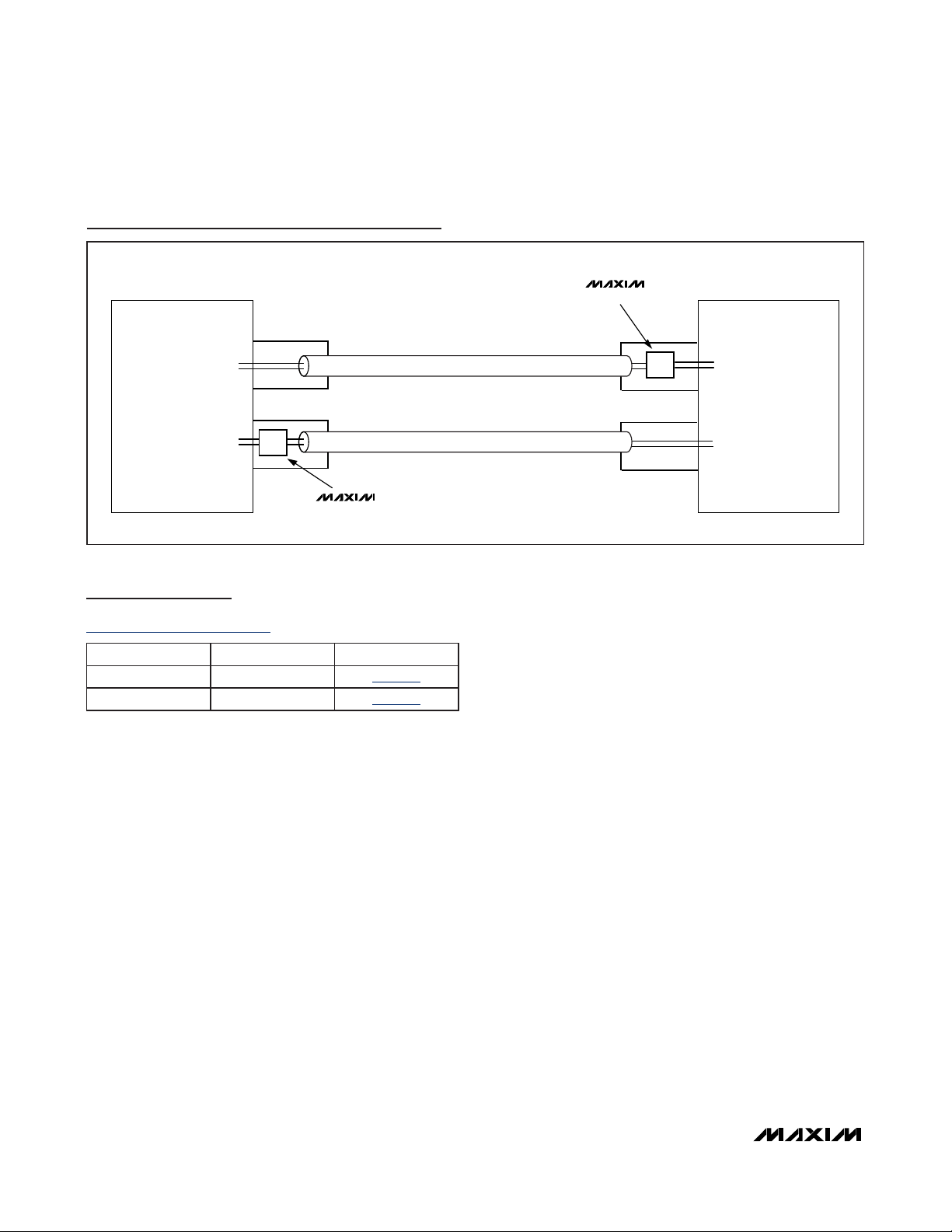
one transceiver module, one for the transmit path and
one for the receive path (see
Typical Application
Circuits
).
UCSP Assembly Considerations
For the latest application details on UCSP construction,
dimensions, tape carrier information, PCB techniques,
bump-pad layout, and recommended reflow temperature profile, as well as the latest information on reliability
testing results, refer to Application Note 1891:
UCSP–A
Wafer-Level Chip-Scale Package
available on Maxim’s
website at www.maxim-ic.com/ucsp.
Chip Information
TRANSISTOR COUNT: 0
PROCESS: SiGe BiPOLAR
Pin Description
Figure 4. Functional Diagram
Figure 5. ESD Protection Diodes
PIN NAME FUNCTION
A1 IN+ Positive Data Input
A3 OUT+ Positive Data Output
C1 IN- Negative Data Input
C3 OUT- Negative Data Output
IN+
MAX3787
IN-
Z1
OUT+
AT 0Hz (DC)
1 = OPEN, Z2 = 0Ω
Z2
Z1
Z
OUT-
MAX3787
IN+
EQUALIZATION
NETWORK
IN-
ESD DIODES
OUT+
OUT-
ESD DIODES
Page 14
MAX3787
14 ______________________________________________________________________________________
1Gbps to 12.5Gbps
Passive Equalizer for Backplanes and Cables
Typical Application Circuits (continued)
Package Information
(For the latest package outline information, go to
www.maxim-ic.com/packages
.)
PACKAGE TYPE PACKAGE CODE DOCUMENT NO.
4 UCSP B9-7
21-0093
4 WLP W91B1+3
21-0067
FIBRE-CHANNEL
HOST BUS ADAPTER
(100Ω) (100Ω)
Rx
EQ
MAX3787
ALL PASSIVE COPPER-CABLE ASSEMBLY
100Ω 24AWG TWIN-AX CABLE
100Ω 24AWG TWIN-AX CABLE
MAX3787
FIBRE-CHANNEL
FABRIC SWITCH
EQ
RxTx(100Ω) (100Ω)
Tx
Page 15

MAX3787
1Gbps to 12.5Gbps
Passive Equalizer for Backplanes and Cables
Maxim cannot assume responsibility for use of any circuitry other than circuitry entirely embodied in a Maxim product. No circuit patent licenses are
implied. Maxim reserves the right to change the circuitry and specifications without notice at any time.
Maxim Integrated Products, 120 San Gabriel Drive, Sunnyvale, CA 94086 408-737-7600 ____________________
15
© 2008 Maxim Integrated Products is a registered trademark of Maxim Integrated Products, Inc.
Revision History
REVISION
NUMBER
0 7/05 Initial release. —
1 12/05 Added lead-free package to Ordering Informat ion table. 1
2 2/08
REVISION
DATE
DESCRIPTION
In the Ordering Information table, changed lead-free part number from ABL+ to
AWL+; added WLP package information.
PAGES
CHANGED
1, 14
 Loading...