

Page 1
MAX3785
6.25Gbps, 1.8V PC Board Equalizer
________________________________________________________________
Maxim Integrated Products
1
19-2630; Rev 4; 10/08
For pricing, delivery, and ordering information, please contact Maxim Direct at 1-888-629-4642,
or visit Maxim’s website at www.maxim-ic.com.
General Description
The MAX3785 6.25Gbps equalizer operates from a single 1.8V supply and compensates for transmissionmedium losses encountered with FR-4 transmission
lines. Optimized for low-voltage, high-density, DC-coupled interconnections between the line card and switch
card, the MAX3785 enables a system upgrade path
while maintaining a legacy rate of 2.5Gbps to
3.125Gbps. Roughly the size of two 0603 passive components, the MAX3785 easily provides placement and
routing flexibility.
The MAX3785 is composed of an equalizer, limiting
amplifier, and output driver. For data rates of 3.2Gbps
and lower, the MAX3785 equalizes signals for spans up
to 40in of FR-4 board material. For data rates up to
6.25Gbps, the MAX3785 compensates for 30in of FR-4
board material. The MAX3785 is coding independent,
functioning equally well for 8b/10b or scrambled signals.
The MAX3785 features DC-coupled current-mode logic
(CML) data inputs and outputs. It is packaged in a tiny
1.5mm ×1.5mm chip-scale package (UCSP™) and a
6-pin TDFN package.
Applications
HSBI for ≤ 6.4Gbps
Double IEEE 802.3ae XAUI
Double STM-16/OC-48
Features
♦ Single 1.8V Supply
♦ Very Low Power, 60mW
♦ Spans 30in with FR-4 at 6.25Gbps
♦ Operates from 1.0Gbps to 6.4Gbps
♦ Coding Independent, 8b/10b or Scrambled
♦ DC-Coupled CML Inputs and Outputs
♦ Small 1.5mm × 1.5mm Footprint
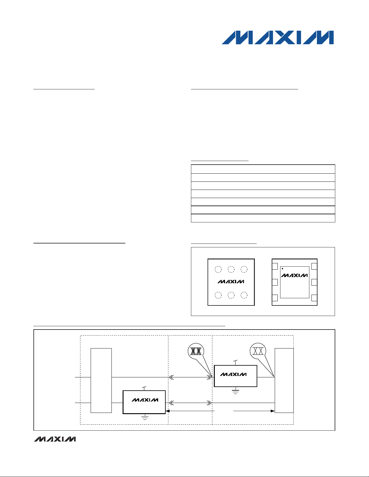
Ordering Information
Typical Application Circuit
UCSP is a trademark of Maxim Integrated Products, Inc.
+
Denotes a lead-free/RoHS-compliant package.
*
EP = Exposed pad.
Pin Configurations
PART TEMP RANGE PIN-PACKAGE
MAX3785UBL 0°C to +85°C 6 UCSP (3 3)
MAX3785UWL+ 0°C to +85°C 6 WLP
MAX3785UTT 0°C to +85°C 6 TDFN-EP*
MAX3785UTT+ 0°C to +85°C 6 TDFN-EP*
MAX3785ITT -20°C to +85°C 6 TDFN-EP*
MAX3785ITT+ -20°C to +85°C 6 TDFN-EP*
TOP VIEW (BUMPS ON BOTTOM OF DIE)
Δ
A1 A2 A3
IN- GND OUT-
MAX3785UBL
C1 C2 C3
IN+ V
3 x 3 UCSP TDFN
OUT+
CC
1 6 IN+
IN-
MAX3785UTT
2
GND
34
5V
CC
OUT+OUT-
LINE CARD
MAC
RxRxTx
1.8V
V
CC
Tx
OUT IN
MAX3785
BACKPLANE
6.25Gbps
IN OUT
MAX3785
30in (0.75m)
1.8V
V
CC
SWITCH CARD
SWITCH
ASIC WITH
SERDES
Rx
Tx
Page 2
MAX3785
6.25Gbps, 1.8V PC Board Equalizer
2 _______________________________________________________________________________________
ABSOLUTE MAXIMUM RATINGS
Stresses beyond those listed under “Absolute Maximum Ratings” may cause permanent damage to the device. These are stress ratings only, and functional
operation of the device at these or any other conditions beyond those indicated in the operational sections of the specifications is not implied. Exposure to
absolute maximum rating conditions for extended periods may affect device reliability.
Supply Voltage, V
CC
to GND.................................-0.5V to +6.0V
Continuous Output Current (OUT+, OUT-) .......-25mA to +25mA
Input Voltage (IN+, IN-) ..............................-0.5V to (V
CC
+ 0.5V)
Operating Ambient Temperature Range
(UBL, UTB)......................................................... 0°C to +85°C
Operating Ambient Temperature Range (ITT).....-20°C to +85°C
Storage Ambient Temperature Range...............-55°C to +150°C
Continuous Power Dissipation (T
A
= +70°C)
6-Pin TDFN (derate 24.4mW above +70°C)..................1.95W
ELECTRICAL CHARACTERISTICS
(Typical values measured at VCC= 1.8V and TA= +25°C. Specifications guaranteed over specified operating conditions.)
(See
Operating Conditions
table.)
Note 1: Guaranteed by design and characterization.
Note 2: Using input pattern 0000011111 at 6.25Gbps.
Note 3: Difference in deterministic jitter between data source and equalizer output, evaluated at 2.5Gbps, 3.2Gbps, 5Gbps, and
6.25Gbps. Pattern used: PRBS (2
7
), ninety-six 0s, 1, 0, 1, 0, PRBS (27), ninety-six 1s, 0, 1, 0, 1.
Note 4: Signal is applied differentially at input to a 6-mil wide, loosely coupled stripline. Deterministic jitter at the output of the
transmission line is from media-induced loss, not from clock source modulation (see Figure 1).
Supply Current 35 55 mA
Input Swing (IN)
Input Common-Mode Voltage Range (Note 1)
Input Return Loss 100MHz to 3.2GHz, power off 15 dB
Differentia l Input Resistance IN+ and IN- 85 100 115
Output Swing
Output Resistance OUT+ or OUT- 42 50 58
Output Return Loss 100MHz to 3.2GHz, IN+ = high 14 dB
Output Transition Time (tr, tf) 20% to 80% (Note 2) 30 40 55 ps
Residual Deterministic Jitter
(Notes 1, 3, 4)
Output Random J itter (Notes 1, 2) 0.75 1.0 ps
Low-Frequency Cutoff Frequenc y 50 kHz
Latency 200 ps
Max imum B it Rate (Note 1) 6.25 6.4 Gbps
Min imum Bit Rate (Note 1) 1.0 2.5 Gbps
PARAMETER CONDITIONS MIN TYP MAX UNITS
Measured differentially at data source before
encountering loss (Point A in Figure 1) (Note 1)
Measured differentially at OUT+ and OUT- with 50
±1% load at each side
2.5Gbps, 3.2Gbps, 5.0Gbps; 0in to 30in FR-4
400mV
2.5Gbps, 3.2Gbps; 40in FR-4
400mV
6.25Gbps; 0in to 30in FR-4
600mV
6.25Gbps; 0in to 30in FR-4
IN = 400mV
IN 1600mV
P-P
IN 1600mV
P-P
IN 1600mV
P-P
P-P
P-P
P-P
P-P
400 1600 mV
(IN
V
CC
MIN
-
/4)
V
-
CC
/4)
(IN
MAX
450 800 mV
0.10 0.15
0.15 0.20
0.15 0.25
0.20 0.30
P-P
V
P-P
UI
RMS
Page 3
MAX3785
6.25Gbps, 1.8V PC Board Equalizer
_______________________________________________________________________________________ 3
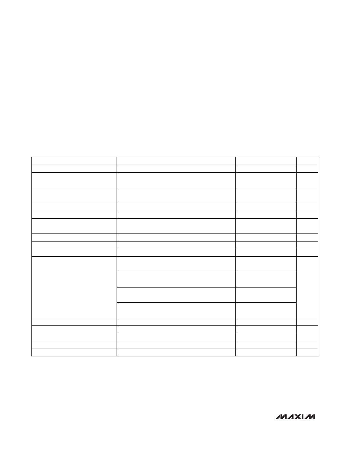
Operating Conditions
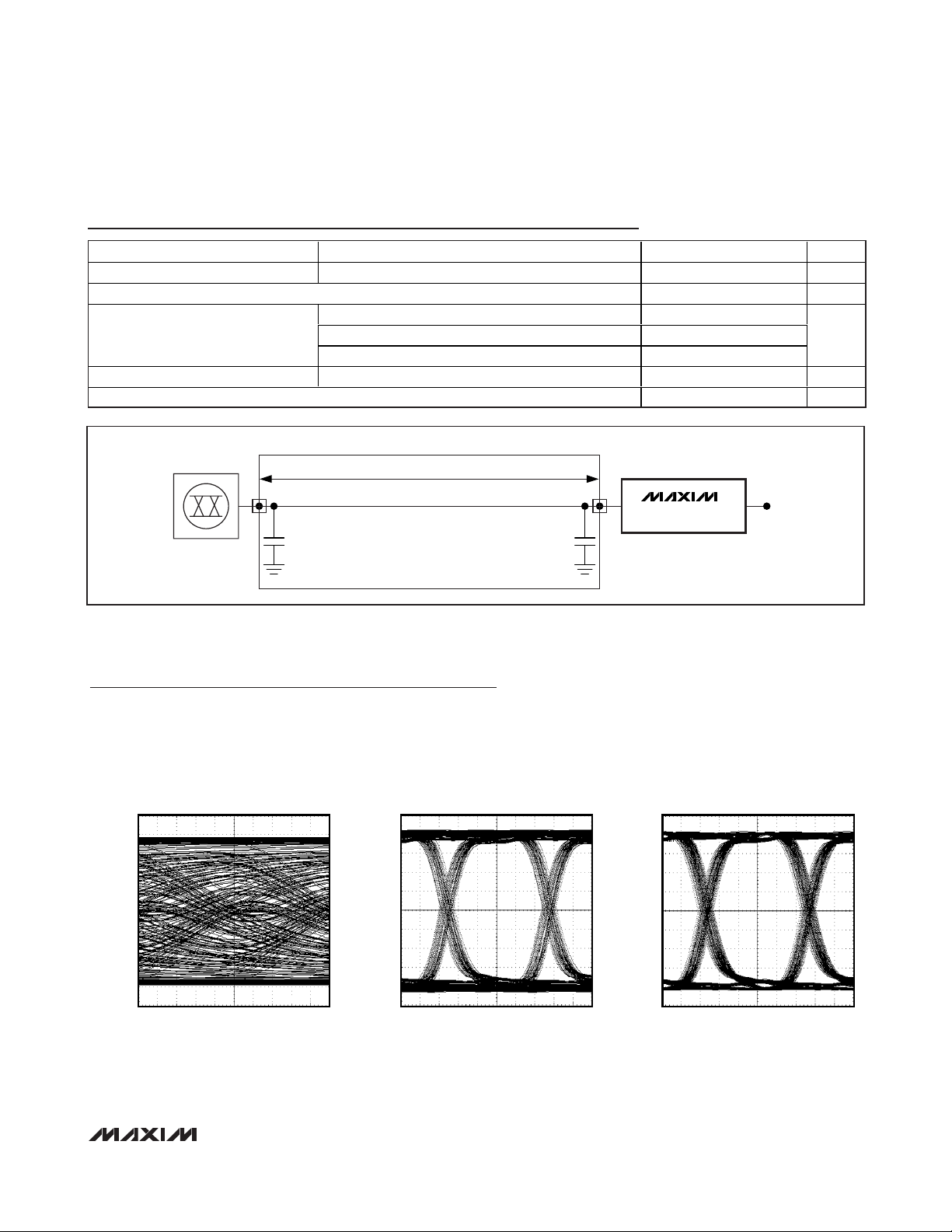
Typical Operating Characteristics
(VCC= +1.8V, TA= +25°C, unless otherwise noted. Measurements done at 6.25Gbps, 500mV
P-P
at the source with a test pattern:
PRBS (2
7
), ninety-six 0s, 1, 0, 1, 0, PRBS (27), ninety-six 1s, 0, 1, 0, 1. Deterministic jitter of the MAX3785 and the board was measured using Tektronix’s FrameScan™. Deterministic jitter of the system was subtracted from the measured value. Eye diagrams were
acquired by FrameScan, which includes system jitter but eliminates random jitter.)
Figure 1. Conditions of Testing
FrameScan is a trademark of Tektronix.
EYE DIAGRAM OF UNEQUALIZED
SIGNAL AFTER 30in OF FR-4
MAX3785 toc01
30ps/div
70mV/div
TEST PATTERN, 6.25Gbps,
WITHOUT RANDOM JITTER,
INCLUDING 13ps SYSTEM JITTER
EYE DIAGRAM OF EQUALIZED
SIGNAL AFTER 30in OF FR-4
MAX3785 toc02
30ps/div
70mV/div
TEST PATTERN, 6.25Gbps,
WITHOUT RANDOM JITTER,
INCLUDING 13ps SYSTEM JITTER
EYE DIAGRAM OF EQUALIZED
SIGNAL AFTER 30in OF FR-4
MAX3785 toc03
30ps/div
70mV/div
2
10
- 1 PRBS, 6.25Gbps,
WITHOUT RANDOM JITTER,
INCLUDING 13ps SYSTEM JITTER
PARAMETER CONDITIONS MIN TYP MAX UNITS
Supply Voltage (VCC) 1.71 1.8 1.89 V
Operating Ambient Temperature (UBL, UTT) 0 25 85 °C
10Hz ≤ f < 100Hz 100
100Hz ≤ f < 1MHz 40Supply Noise Tolerance
1MHz ≤ f ≤ 1GHz 10
Bit Rate NRZ data 2.50 6.25 Gbps
Operating Ambient Temperature (ITT) -20 25 85 °C
PC BOARD
SIGNAL SOURCE
AB
<1.0pF SMA
CONNECTOR
3in ≤ L ≤ 30in
<1.0pF SMA
CONNECTOR
IN OUT
MAX3785
FR-4
< 4.4
4.0 < ε
r
tanδ = 0.022
C
mV
P-P
Page 4

MAX3785
6.25Gbps, 1.8V PC Board Equalizer
4 _______________________________________________________________________________________
Typical Operating Characteristics (continued)
(VCC= +1.8V, TA= +25°C, unless otherwise noted. Measurements done at 6.25Gbps, 500mV
P-P
at the source with a test pattern:
PRBS (2
7
), ninety-six 0s, 1, 0, 1, 0, PRBS (27), ninety-six 1s, 0, 1, 0, 1. Deterministic jitter of the MAX3785 and the board was measured
using Tektronix’s FrameScan. Deterministic jitter of the system was subtracted from the measured value. Eye diagrams were acquired
by FrameScan, which includes system jitter but eliminates random jitter.)
EYE DIAGRAM OF UNEQUALIZED
SIGNAL AFTER 30in OF FR-4
MAX3785 toc04
50ps/div
70mV/div
TEST PATTERN, 3.125Gbps,
WITHOUT RANDOM JITTER,
INCLUDING 13ps SYSTEM JITTER
EYE DIAGRAM OF EQUALIZED
SIGNAL AFTER 30in OF FR-4
MAX3785 toc05
50ps/div
70mV/div
TEST PATTERN, 3.125Gbps,
WITHOUT RANDOM JITTER,
INCLUDING 13ps SYSTEM JITTER
EYE DIAGRAM OF EQUALIZED
SIGNAL AFTER 30in OF FR-4
MAX3785 toc06
50ps/div
70mV/div
CRPAT, 3.125Gbps,
WITHOUT RANDOM JITTER,
INCLUDING 13ps SYSTEM JITTER
EQUALIZER OPERATING CURRENT
vs. TEMPERATURE
MAX3785 toc07
TEMPERATURE (°C)
CURRENT (mA)
807050 6020 30 4010
10
20
30
40
50
60
70
80
90
100
0
0
DETERMINISTIC JITTER
vs. BOARD LENGTH (FR-4)
(INPUT LEVEL OF 500mV
P-P
, TEST PATTERN)
MAX3785 toc08
BOARD LENGTH (in)
JITTER (ps)
3530252015
10
15
20
25
30
35
40
45
50
55
60
65
5
10 40
2.5Gbps
6Gbps
3.125Gbps
5Gbps
DETERMINISTIC JITTER vs. SIGNAL LEVEL
(TEST PATTERN, 30in OF FR-4 BOARD)
MAX3785 toc09
DIFFERENTIAL SIGNAL LEVEL (V
P-P
)
JITTER (ps)
1.81.61.41.21.00.80.6
5
10
15
20
0
0.4 2.0
3.125Gbps
2.5Gbps
6.4Gbps
5Gbps
Page 5

MAX3785
6.25Gbps, 1.8V PC Board Equalizer
_______________________________________________________________________________________
5
Typical Operating Characteristics (continued)
(VCC= +1.8V, TA= +25°C, unless otherwise noted. Measurements done at 6.25Gbps, 500mV
P-P
at the source with a test pattern:
PRBS (2
7
), ninety-six 0s, 1, 0, 1, 0, PRBS (27), ninety-six 1s, 0, 1, 0, 1. Deterministic jitter of the MAX3785 and the board was measured
using Tektronix’s FrameScan. Deterministic jitter of the system was subtracted from the measured value. Eye diagrams were acquired
by FrameScan, which includes system jitter but eliminates random jitter.)
DETERMINISTIC JITTER vs. DATA RATE
FOR 10in OF FR-4 BOARD
(INPUT LEVEL OF 500mV
P-P
)
MAX3785 toc10
DATA RATE (Gbps)
JITTER (ps)
6.55.54.53.5
5
10
15
20
25
30
0
2.5
210 - 1
27 - 1
TEST
PATTERN
K28.5
CRPAT
DETERMINISTIC JITTER vs. DATA RATE
FOR 20in OF FR-4 BOARD
(INPUT LEVEL OF 500mV
P-P
)
MAX3785 toc11
DATA RATE (Gbps)
JITTER (ps)
6.55.54.53.5
5
10
15
20
25
30
0
2.5
210 - 1
27 - 1
TEST
PATTERN
K28.5
CRPAT
DETERMINISTIC JITTER vs. DATA RATE
FOR 30in OF FR-4 BOARD
(INPUT LEVEL OF 500mV
P-P
)
MAX3785 toc12
DATA RATE (Gbps)
JITTER (ps)
6.55.54.53.5
5
10
15
20
25
30
0
2.5
210 - 1
27 - 1
TEST PATTERN
K28.5
CRPAT
EQUALIZER INPUT RETURN GAIN (SDD11)
(INPUT SIGNAL LEVEL = -40dBm, POWER OFF)
MAX3785 toc13
FREQUENCY (MHz)
GAIN (dB)
1000
-30
-20
-10
0
10
20
30
-40
100 10,000
EQUALIZER INPUT RETURN GAIN (SDD22)
(INPUT SIGNAL LEVEL = -40dBm, IN+ HIGH)
MAX3785 toc14
FREQUENCY (MHz)
GAIN (dB)
1000
-30
-20
-10
0
10
20
30
-40
100 10,000
Page 6

MAX3785
Functional Description
The MAX3785 6.25Gbps PC board equalizer consists
of an equalizer, limiting amplifier, offset driver, and offset cancellation circuit (see Figure 2). The equalizer
block compensates for the attenuation caused by the
PC board. The limiting amplifier squares up the signal
at the output of the equalizer block. The offset cancellation circuit corrects for internal offset in the limiting
amplifier to minimize pulse-width distortion. This introduces a low-frequency cutoff. The data must achieve a
50% mark/space ratio in less than 100µs. The specified
minimum differential input must be maintained to avoid
oscillation.
Input and Output Structures
An equivalent DC input circuit is shown in Figure 3. It
has an equivalent DC differential input resistance of
100Ω. The output buffer is implemented using currentmode logic (CML), as shown in Figure 4.
Package Description
The chip-scale package (UCSP) has a bump pitch of
0.5mm (19.7 mils) and a bump diameter of 0.3mm (12
mils). Lay out the solder pad spacing on 0.5mm (19.7
mils), a pad size of 0.25mm (10 mils) and a solder
mask opening of 0.33mm (13 mils). Round or square
pads are permissible. For detailed information on UCSP
layout and handling, go to Maxim’s website,
www.maxim-ic.com
. The enclosed package description was accurate at the time of publication. For the
MAX3785, all the balls shown in row B of the drawing
are unpopulated. See the
Package Information
section
for the latest package information.
6.25Gbps, 1.8V PC Board Equalizer
6 _______________________________________________________________________________________
MAX3785UBL Pin Description
MAX3785UTT Pin Description
Figure 2. Functional Diagram of the MAX3785
PIN NAME FUNCTION (MAX3785UBL)
A1 IN- Negative Data Input, CML
A2 GND Supply Ground
A3 OUT- Negative Data Output, CML
C1 IN+ Positive Data Input, CML
C2 VCC Supply Voltage
C3 OUT+ Positive Data Output, CML
IN+
IN-
PIN NAME FUNCTION (MAX3785UTT)
1 IN- Negative Data Input (CML)
2 GND Supply Ground
3 OUT- Negative Data Output (CML)
4 OUT+ Posit ive Data Output (CML)
5 VCC Supply Voltage
6 IN+ Positive Data Input (CML)
— EP Exposed Pad
EQUALIZER
MAX3785
LIMITER
OFFSET
ADJUST
OUTPUT
BUFFER
OUT+
OUT-
Page 7

MAX3785
6.25Gbps, 1.8V PC Board Equalizer
_______________________________________________________________________________________ 7
Figure 3. Equalizer Input DC Equivalent Circuit
Figure 4. CML Output Equivalent Circuit
Package Information
For the latest package outline information and land patterns, go
to www.maxim-ic.com/packages
.
PACKAGE TYPE PACKAGE CODE DOCUMENT NO.
6 UCSP B9-3
21-0093
6 WLP W91B1+2
21-0067
6 TDFN T633-2
21-0137
IN+
IN-
ESD
STRUCTURES
V
CC
37Ω 37Ω
28Ω
37Ω 37Ω
V
CC
50Ω 50Ω
OFFSET
CORRECTION
50Ω 50Ω
OUT+
OUT-
ESD
STRUCTURES
Page 8

MAX3785
6.25Gbps, 1.8V PC Board Equalizer
Maxim cannot assume responsibility for use of any circuitry other than circuitry entirely embodied in a Maxim product. No circuit patent licenses are
implied. Maxim reserves the right to change the circuitry and specifications without notice at any time.
8
_____________________Maxim Integrated Products, 120 San Gabriel Drive, Sunnyvale, CA 94086 408-737-7600
© 2008 Maxim Integrated Products is a registered trademark of Maxim Integrated Products, Inc.
Revision History
REVISION
NUMBER
0 10/02 Initial release. —
1 8/03 Added the MAX3785UTT (6-pin TDFN) package. 1, 2, 6, 9
2 5/04 Added the MAX3785ITT (“I” temperature grade range for -20°C to +85°C). 1, 2, 3
REVISION
DATE
DESCRIPTION
PAGES
CHANGED
3 12/05 Updated the Ordering Information table to include lead-free packages. 1
4 10/08 Updated the Ordering Information table to include the WLP package. 1
 Loading...