

General Description
The MAX3784/MAX3784A 5Gbps equalizers provide
compensation for transmission-medium losses in up to
40in of FR-4. They are optimized for short-run length
and balanced codes such as 8b10b, as found in multiplexed 1.25Gbps Ethernet systems and 4.25Gbps
Fibre Channel.
The equalizers use differential CML data inputs and
outputs. A standby mode reduces power consumption
when the parts are not in use. The MAX3784/
MAX3784A are available in a 4mm × 4mm, 16-pin QFN
package that consumes only 185mW at +3.3V.
Features
♦ Spans 40in (1m) of FR-4 PCB
♦ 0.18UI Deterministic Jitter Up to 40in
♦ Low Power Consumption: 185mW (MAX3784)
♦ Equalization Reduces Intersymbol Interference
♦ Single +3.3V Supply
♦ Standby Mode
♦ Small 4mm × 4mm, 16-Pin QFN Package
MAX3784/MAX3784A
5Gbps PCB Equalizer
________________________________________________________________
Maxim Integrated Products
1
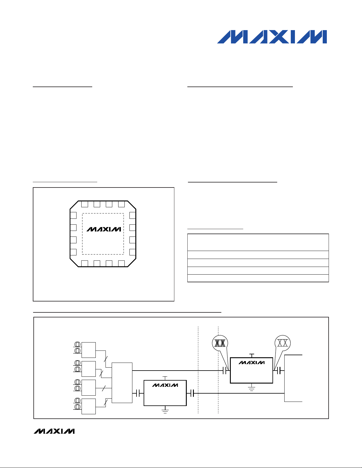
Pin Configurations
LINE CARD
+3.3V
5Gbps
+3.3V
T/R 1
Rx
Tx
T/R 2
Rx
Tx
T/R 3
Rx
Tx
T/R 4
Rx
Tx
T/R 1
T/R 2
T/R 3
T/R 4
Rx
Tx
1.25Gbps
1.25Gbps
1.25Gbps
1.25Gbps
SWITCH
Rx
Tx
SWITCH CARD
PCB
BACKPLANE
MAX3784/
MAX3784A
EQUALIZER
IN OUT
MAX3784/
MAX3784A
EQUALIZER
OUT IN
Typical Application Circuit
19-2565; Rev 4; 10/07
For pricing, delivery, and ordering information, please contact Maxim Direct at 1-888-629-4642,
or visit Maxim’s website at www.maxim-ic.com.
Ordering Information
Applications
Chassis Life Extension
4.25Gbps Fibre Channel
4x Multiplexed 1.25Gbps Ethernet (5Gbps)
+
Denotes a lead-free package.
*Exposed pad.
1
23
4
5
6
7
8
9
10
11
16
12
13
14
15
V
CC
V
CC
V
CC
IN+
IN-
GND
GND
GND
N.C.
N.C.
N.C.
N.C.
N.C.
EN
OUT+
OUT-
* THE EXPOSED PAD MUST BE SOLDERED TO SUPPLY GROUND
FOR CORRECT THERMAL AND ELECTRICAL PERFORMANCE.
MAX3784/
MAX3784A
TOP VIEW
QFN
*EP
Pin Configurations continued at end of data sheet.
PART
TEMP
RANGE
MAX3784UGE 0°C to +85°C 16 QFN-EP* G1644-1
MAX3784UTE+ 0°C to +85°C 16 TQFN-EP* T1644-3
MAX3 784AUGE 0°C to +85°C 16 QFN-EP* G1644-1
MAX3784AUTE+ 0°C to +85°C 16 TQFN-EP* T1644-3
PINPACKAGE
PKG
CODE
MAX3784/MAX3784A
5Gbps PCB Equalizer
2 _______________________________________________________________________________________
ABSOLUTE MAXIMUM RATINGS
ELECTRICAL CHARACTERISTICS
(VCC= +3V to +3.6V, TA= 0°C to +85°C. Typical values are at VCC= +3.3V and TA= +25°C, unless otherwise noted.)
Stresses beyond those listed under “Absolute Maximum Ratings” may cause permanent damage to the device. These are stress ratings only, and functional
operation of the device at these or any other conditions beyond those indicated in the operational sections of the specifications is not implied. Exposure to
absolute maximum rating conditions for extended periods may affect device reliability.
Supply Voltage, VCC.................................................-0.5V to +6V
Input Voltage............................................(-0.5V) to (V
CC
+ 0.5V)
Continuous Output Current ...............................-25mA to +25mA
Continuous Power Dissipation (T
A
= +85°C)
16-Pin QFN (derate 25mW/°C above +85°C) ............1600mW
Operating Ambient Temperature Range ................0°C to +85°C
Storage Temperature Range .............................-55°C to +150°C
Lead Temperature (soldering, 10s) .................................+300°C
Supply Power
PARAMETER SYMBOL CONDITIONS MIN TYP MAX UNITS
EN = low 30
EN = high 185 250
Latency From input to output 200 ps
CML RECEIVER INPUT
Input Voltage Swing V
Return Loss 100MHz to 2.5GHz 15 dB
Input Resistance Differential 80 100 120 Ω
EQUALIZATION
Residual Deterministic Jitter,
5Gbps
Residual Deterministic Jitter,
2.5Gbps
Residual Deterministic Jitter,
1.25Gbps
Random Jitter (Notes 5, 6) 1.3 1.9 ps
CML TRANSMITTER OUTPUT (into 100Ω ±1Ω)
Output Voltage Swing V
Transition Time t
Output Resistance Single ended 40 50 60 Ω
f, tr
Measured differentially at point A in Figure 1 400 1000 mV
IN
Table 1 (Notes 2–5)
Table 1 (Notes 2–5)
Table 1 (Notes 2–5)
Differential swing, measured
O
differentially at point C in Figure 1
20% to 80% (Notes 5, 8) 30 45 60 ps
10Hz < f < 100Hz 100
100Hz < f < 1MHz 40Supply-Noise Tolerance (Note 1)
1MHz < f < 2.5GHz 10
20in 0.13 0.21
40in 0.18 0.23
20in 0.08 0.14
40in 0.13 0.28
20in 0.04 0.07
40in 0.07 0.15
MAX3784 400 600
MAX3784A 550 750
mV
UI
UI
UI
mV
mW
P-P
P-P
P-P
P-P
P-P
RMS
P-P
MAX3784/MAX3784A
5Gbps PCB Equalizer
_______________________________________________________________________________________ 3
ELECTRICAL CHARACTERISTICS (continued)
(VCC= +3V to +3.6V, TA= 0°C to +85°C. Typical values are at VCC= +3.3V and TA= +25°C, unless otherwise noted.)
Note 1: Allowed supply noise during jitter tests.
Note 2: Test pattern. This is a combination of K28.5± characters running at the full bit rate and at one-quarter the bit rate. This simu-
lates the multiplexing of four each 1.25Gbps Ethernet data streams.
Pattern (hex) 100 bits
00 FFFF F0F0 FF 0000 0F0F (quarter rate K28.5+, quarter rate K28.5-)
3EB05 (K28.5± 00 1111 1010 11 0000 0101)
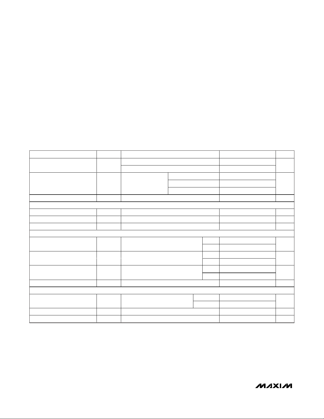
Note 3: Difference in deterministic jitter between reference points A and C in Figure 1.
Note 4: Signal source amplitude range is 400mV
P-P
to 1000mV
P-P
differential. Signal is applied differentially at point A as shown in
Figure 1. The deterministic jitter at point B must be from media-induced loss and not from clock-source modulation.
Deterministic jitter is measured at the 50% vertical level of the signal at point C.
Note 5: Guaranteed by design and characterization.
Note 6: Test pattern is K28.5 with 40in trace.
Note 7: On-chip pullup resistor of 40kΩ (typ). Negative current indicates equalizer sources current.
Note 8: Using 00 0001 1111 or equivalent pattern. Measured over entire input voltage range, max and min media loss and within 2in
of output pins.
Figure 1. Test Conditions
Table 1. PCB Assumptions (PCB material is FR-4)
ENABLE CONTROL PIN
Input High Voltage 1.5 V
Input Low Voltage 0.5 V
Input High Current (Note 7) -150 +10 µA
Input Low Current (Note 7) -150 +10 µA
PARAMETER SYMBOL CONDITIONS MIN TYP MAX UNITS
SIGNAL
SOURCE
A
SMA CONNECTOR
BACKPLANE PCB
6mil LINE
L ≤ 40in
SMA CONNECTOR
BC
MAX3784/MAX3784A
EQUALIZER
IN OUT
PARAMETER CONDITIONS MIN TY P MAX UNITS
Transm issi on Line Edge-coupled stripline 6 mi ls
Relative Permitti vity FR-4 or sim ilar 4.4 4.5 —
Los s Tangent FR-4 or simi lar 0.02 0.022 —
Metal Thickne ss 0.7 mi ls (0.5o z copper) 0.7 mils
Impedance Different ia l 90 100 110

MAX3784/MAX3784A
5Gbps PCB Equalizer
4 _______________________________________________________________________________________
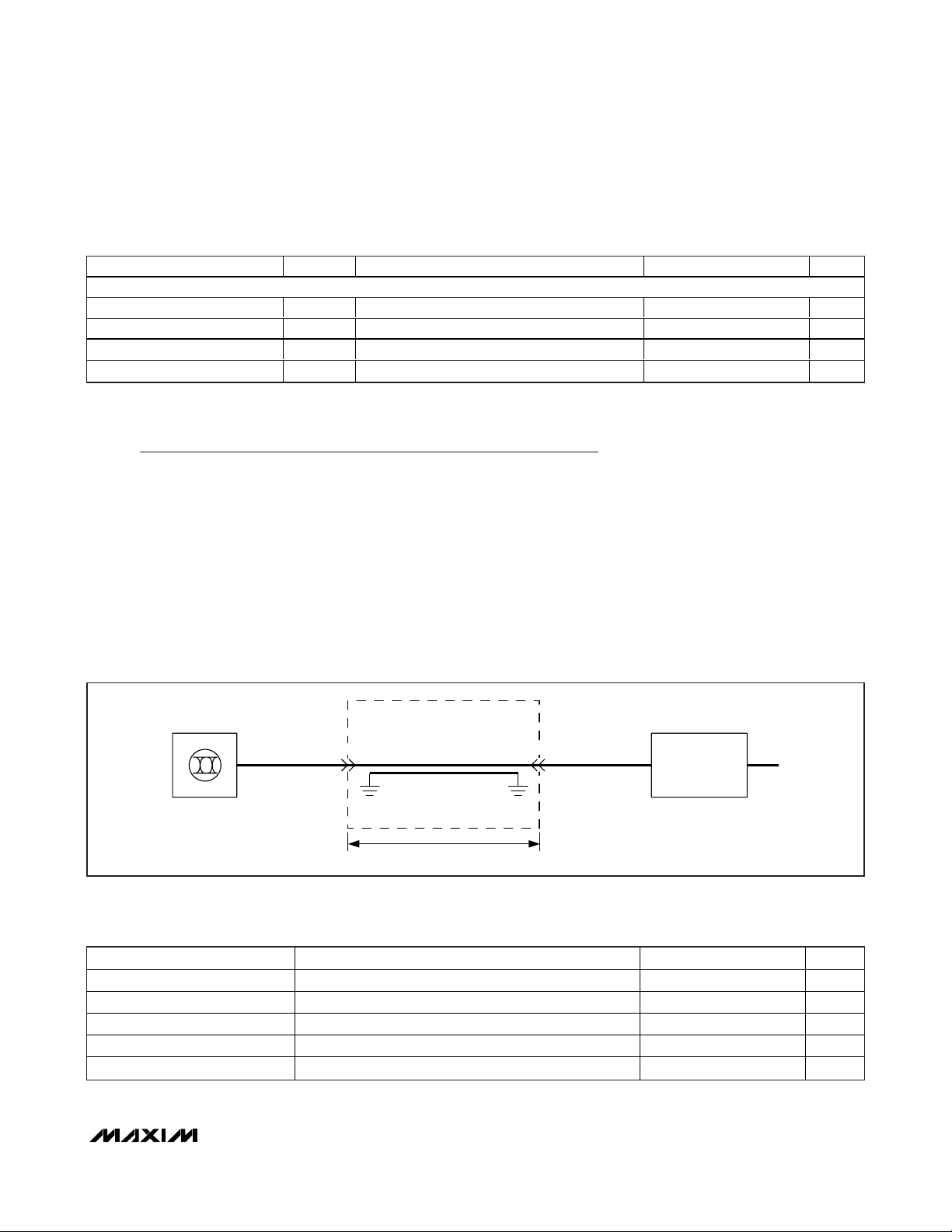
Typical Operating Characteristics
(VCC= +3.3V, measurements done at 5Gbps, 800mV
P-P
board input with 100-bit pattern from Note 2 of the
EC Table
,TA= +25°C,
unless otherwise noted.)
55mV/
div
EQUALIZER INPUT EYE DIAGRAM
BEFORE EQUALIZATION AT 5Gbps
(40in, FR-4, 6-mil STRIPLINE)
MAX3784/4A toc01
32ps/div
80mV/
div
EQUALIZER OUTPUT EYE DIAGRAM
AFTER EQUALIZATION AT 5Gbps
(40in, FR-4, 6-mil STRIPLINE, MAX3784)
MAX3784/4A toc02
35ps/div
80mV/
div
EQUALIZER OUTPUT EYE DIAGRAM
AFTER EQUALIZATION AT 5Gbps
(40in, FR-4, 6-mil STRIPLINE, MAX3784A)
MAX3784/4A toc03
35ps/div
0
10
5
20
15
25
30
05
DIFFERENTIAL RETURN LOSS
MAX3784/4A toc04
FREQUENCY (GHz)
RETURN LOSS (dB)
2134
0
30
20
10
40
50
60
70
80
90
100
02010 30 40 50 60
DETERMINISTIC JITTER
vs. LINE LENGTH
MAX3784/4A toc05
LINE LENGTH (in)
(FR-4 6-mil STRIPLINE)
DETERMINISTIC JITTER (ps)
1.25GHz
2.5GHz
5GHz
0
30
20
10
40
50
60
70
80
90
100
200 600400 800 1000 1200
DETERMINISTIC JITTER vs. AMPLITUDE
(20in FR-4 STRIPLINE)
MAX3784/4A toc06
INPUT AMPLITUDE (mV
P-P
)
(FIGURE 1, POINT A)
DETERMINISTIC JITTER (ps)
1.25GHz
2.5GHz
5GHz
0
30
20
10
40
50
60
70
80
90
100
200 600400 800 1000 1200
DETERMINISTIC JITTER vs. AMPLITUDE
(40in FR-4 STRIPLINE)
MAX3784/4A toc07
INPUT AMPLITUDE (mV
P-P
)
(FIGURE 1, POINT A)
DETERMINISTIC JITTER (ps)
1.25GHz
2.5GHz
5GHz
0
100
300
200
400
500
LATENCY vs. TEMPERATURE
MAX3784/4A toc08
TEMPERATURE (°C)
LATENCY (ps)
05025 75 100
0
10
20
30
40
50
60
70
80
0255075
SUPPLY CURRENT vs. TEMPERATURE
MAX3784/4A toc09
TEMPERATURE (°C)
SUPPLY CURRENT (mA)
I
CC
MAX3784
I
CC
MAX3784A
I
SHUTDOWN
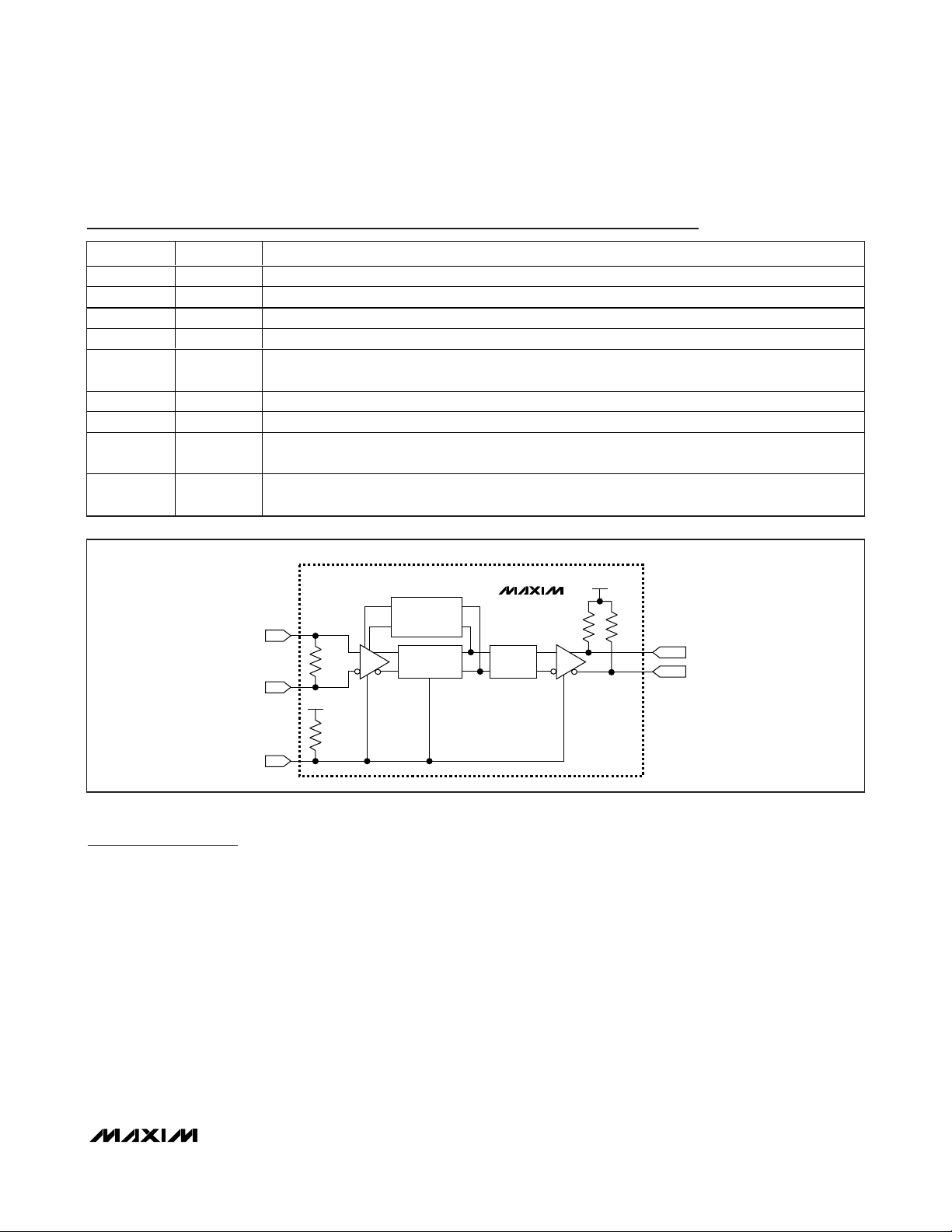
Detailed Description
General Theory of Operation
The MAX3784/MAX3784A adaptive equalizers extend
the reach of transmission lines in high-frequency backplane interconnect applications. They can be used for
4.25Gbps Fibre Channel, 4x 1.25Gbps Ethernet (5Gbps)
and other NRZ, 8b10b or short (≤ 20 bits) CID data
types. Internally, the MAX3784/MAX3784A are comprised of an equalizer control loop and limiting output
driver. The equalizer block reduces intersymbol interference (ISI), compensating for frequency-dependent
media-induced loss. The equalization control detects the
spectral contents of the input signal and provides a control voltage to the equalizer core, adapting it to different
media. The equalizer operation is optimized for short-run,
DC-balanced transmission codes.
Standby Mode
Standby saves power when the equalizer is not in use.
The EN logic input must be set high or open for normal
operation. Logic low at EN forces the equalizer into the
standby state.
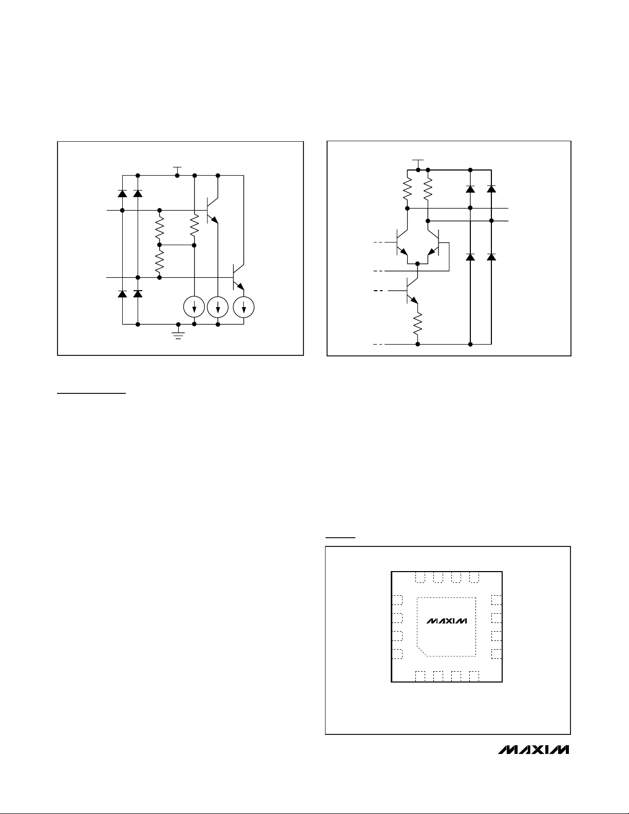
CML Input and Output Buffers
The input and output buffers are implemented using current-mode logic (CML). Equivalent circuits are shown in
Figures 3 and 4. For details on interfacing with CML,
refer to Maxim Application Note HFAN-01.0:
Introduction
to LVDS, PECL, and CML
. The common-mode voltage
of the input and output is above +2.5V. AC-coupling
capacitors are required when interfacing this part with
devices terminated in voltages such as +1.8V. Values of
0.10µF or greater are recommended.
MAX3784/MAX3784A
5Gbps PCB Equalizer
_______________________________________________________________________________________________________ 5
Pin Description
Figure 2. Functional Diagram
PIN NAME FUNCTION
1, 7, 12 V
2 IN+ Positive Input, CML
3 IN- Negative Input, CML
4, 6, 9 GND Supply Ground
5, 8, 14, 15,
16
10 OUT- Negative Output, CML
11 OUT+ Positive Output, CML
13 EN
EP
CC
N.C. No Connection. Leave unconnected.
Exposed
Pad
+3.3V Supply Voltage
Enable Equalizer. A logic high or open selects normal operation. A logic low selects low-power
standby mode.
Connect to Ground. The exposed pad must be soldered to the circuit board ground plane for proper
thermal and electrical performance.
5Gbps EQUALIZER
OFFSET
CANCELLATION
IN+
100Ω
IN-
V
CC
LOWPASS FILTER
EQUALIZER
MAX3784/
MAX3784A
LIMITER
50Ω
V
CC
50Ω
OUT+
OUT-
40kΩ
EN
MAX3784/MAX3784A
Applications Information
Alternate Data Rates
The MAX3784/MAX3784A is optimized for automatic
operation at 5Gbps. Equalization at other data rates,
such as 1.25Gbps and 2.5Gbps, is possible. See the
Typical Operating Characteristics
for Deterministic Jitter
vs. Line Length and Deterministic Jitter vs. Amplitude
for typical performance at these data rates.
Layout Considerations
Circuit board layout and design can significantly affect
the MAX3784/MAX3784As’ performance. Use good
high-frequency design techniques, including minimizing ground inductance and connections and using controlled-impedance transmission lines for the
high-frequency data signals. Route signals differentially
to reduce EMI susceptibility and crosstalk. Solder the
exposed pad to supply ground for proper thermal and
electrical operation.
Place power-supply decoupling capacitors as close as
possible to the VCCpins.
5Gbps PCB Equalizer
6 _______________________________________________________________________________________
Figure 3. CML Input Equivalent Circuit
Figure 4. CML Output Equivalent Circuit
15
16
14
13
6
5
7
IN+
GND
8
V
CC
OUT+
GND
V
CC
12
N.C.
4
12 11 9
N.C.
N.C.
N.C.
V
CC
GND
N.C.
MAX3784
MAX3784A
IN- OUT-
3
10
EN
TQFN
TOP VIEW
* THE EXPOSED PAD MUST BE SOLDERED TO SUPPLY GROUND
FOR CORRECT THERMAL AND ELECTRICAL PERFORMANCE.
*EP
+
Pin Configurations (continued)
V
CC
50Ω
50Ω
250μA
V
CC
50Ω 50Ω
OUT+
OUT-
21-0139
MAX3784/MAX3784A
5Gbps PCB Equalizer
Maxim cannot assume responsibility for use of any circuitry other than circuitry entirely embodied in a Maxim product. No circuit patent licenses are
implied. Maxim reserves the right to change the circuitry and specifications without notice at any time.
Maxim Integrated Products, 120 San Gabriel Drive, Sunnyvale, CA 94086 408-737-7600 _____________________
7
© 2007 Maxim Integrated Products is a registered trademark of Maxim Integrated Products.
Revision History
Pages changed at Rev 4: 1–7 (removed package drawings, replaced with table)
Package Information
For the latest package outline information, go to
www.maxim-ic.com/packages
.
PACKAGE TYPE DOCUMENT NO.
16 QFN
21-0106
16 TQFN
 Loading...