

Page 1
General Description
The MAX3783 is a dual serial multiplexer (mux) and
buffer with selectable line-side loopback for system
interconnect and serial backplane applications up to
2.7Gbps. Each independent channel consists of a transmitter with fanout of two and a receiver with a 2:1 input
mux. Selectable loopback paths support system testing.
Operating from a single 3.3V supply, this device has
current-mode logic (CML) inputs and outputs, which
can be AC-coupled for PECL compatibility, if desired.
The IC is packaged in a compact 48-pin TQFP-EP package with exposed pad. Typical power consumption is
1.12W.
Applications
2.7Gbps Serial Communications
System Interconnect
Serial Backplane
Fail-Over and Protection Switching
Features
♦ Provides Redundant Serial I/O
♦ 11ps Deterministic Jitter
♦ Selectable Loopback
♦ On-Chip 50Ω Termination Resistors
♦ 3.3V Power Supply
♦ Two-Port Integration
MAX3783
2.7Gbps Dual Mux/Buffer with Loopback
Pin Configuration
Ordering Information
19-2197; Rev 2; 1/08
Typical Application Circuit appears at end of data sheet.
EVALUATION KIT
AVAILABLE
*EP = Exposed pad.
+
Denotes a lead-free package.
________________________________________________________________
Maxim Integrated Products
1
For pricing, delivery, and ordering information, please contact Maxim Direct at 1-888-629-4642,
or visit Maxim’s website at www.maxim-ic.com.
PART TEMP RANGE PIN-PACKAGE
MAX3783UCM 0°C to +85°C 48 TQFP-EP*
MAX3783UCM+ 0°C to +85°C 48 TQFP-EP*
SELA
VCCSOA+
SOA-
4847464544434241403938
1
GND
2
SIA-
3
SIA+
4
V
CC
5
LB1A
6
LB2A
7
LB1B
8
LB2B
9
V
CC
10
SIB+
11
SIB-
12
GND
1314151617181920212223
CC
V
SELB
SOB+
SOB-
TQFP-EP*
*EXPOSED PAD MUST BE SOLDERED TO SUPPLY GROUND ON THE CIRCUIT BOARD.
VCCLO1A+
LO1A-
VCCLO2A+
LO2A-
VCCGND
37
36
35
34
33
32
MAX3783
CC
V
LO1B+
LO1B-
CC
V
LO2B-
LO2B+
31
30
29
28
27
26
25
24
CC
V
GND
LI2A+
LI2AV
CC
LI1A+
LI1AGND
GND
LI1BLI1B+
V
CC
LI2BLI2B+
Page 2
MAX3783
2.7Gbps Dual Mux/Buffer with Loopback
2 _______________________________________________________________________________________
ABSOLUTE MAXIMUM RATINGS
ELECTRICAL CHARACTERISTICS
(VCC= 3.0V to 3.6V, serial data rate = 2.75Gbps, TA= 0°C to +85°C. Typical values at VCC= 3.3V, TA= +25°C, unless otherwise
noted.)
Stresses beyond those listed under “Absolute Maximum Ratings” may cause permanent damage to the device. These are stress ratings only, and functional
operation of the device at these or any other conditions beyond those indicated in the operational sections of the specifications is not implied. Exposure to
absolute maximum rating conditions for extended periods may affect device reliability.
Note 2: Tested using a repeating 1010 pattern at 500Mbps.
Note 3: AC specifications are guaranteed by design and characterization.
Note 4: Deterministic jitter is measured with a repeating K28.5 pattern.
Note 5: With the peak-to-peak input swing on the selected (transmitted) CML input equal to or greater than that on the nonselected
inputs.
Note 6: AC specifications are guaranteed by test.
Supply Voltage, V
CC
...............................................-0.5V to 4.0V
Continuous Current at Serial Outputs...............................±36mA
Voltage at SEL_, LB_ Pins ..........................-0.5V to (V
CC
+ 0.5V)
Common-Mode Input Voltage (SI_, LI_) .....-0.5V to (V
CC
+ 0.5V)
Differential Input Voltage (SI_, LI_) (Note 1) .......................±2.8V
Continuous Power Dissipation (T
A
= +85°C)
48-Pin TQFP-EP (derate 27mW/°C above +85°C) .........1.76W
Storage Ambient Temperature ..........................-55°C to +150°C
Lead Temperature (soldering, 10s) .................................+300°C
Note 1: The sum of the common-mode voltage and differential voltage on any input pin must be within -0.5V to (V
CC
+ 0.5V).
PARAMETER S YMBOL CONDITIONS MIN TYP MAX UNITS
Max imum Serial Data Rate 2.75 3.125 Gbps
Power Dis sipation AC-coupled inputs, outputs 1.12 1.68 W
Supply Current ICC 340 466 mA
CML Differential Output Voltage VOD RL = 50 to VCC, or 100 differential (Note 2) 1200 1500 2200 mVp-p
CML Differential Input Voltage VID 200 1600 2200 mVp-p
CML Output Impedance R
CML Input Impedance RIN Differential 85 100 116
Random Jitter (Note 3) 1 2 ps
Determin istic Jitter (Notes 3, 4, 5) 11 25 ps
CML Output Edge Speed
(20% to 80%)
Propagation Delay LI_ to SO_, SI_ to LO_, LI _ to LO_ (Note 3) 340 500 ps
Multiplexer Switch Time SEL_ or LB_ to valid output 9 ns
TTL Input Current High VIH = +2.0V to (VCC +0.3V) 180 μA
TTL Input Current Low VIL = -0.3V to +0.8V 440 μA
Single ended 42.5 50 57.5
OUT
t
, t
R
2.5Gbps input (Note 6) 70 135
F
1.25Gbps input (Note 3) 80 200
RMS
p-p
ps
Page 3
MAX3783
2.7Gbps Dual Mux/Buffer with Loopback
_______________________________________________________________________________________
3
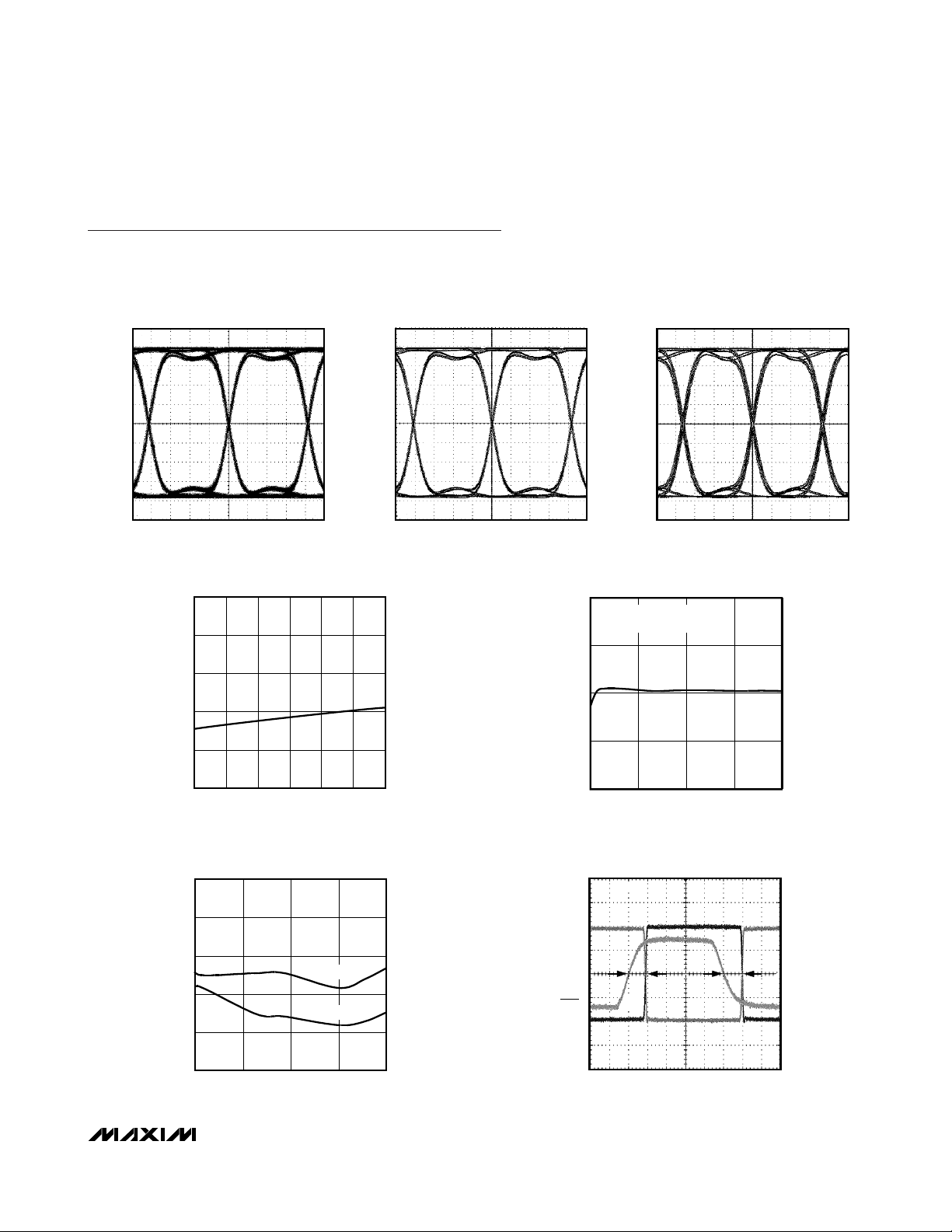
Typical Operating Characteristics
(VCC= 3.3V, TA = +25°C, unless otherwise noted.)
ELECTRICAL EYE DIAGRAM
23
- 1 PRBS PATTERN
MAX3783 toc01
195mV/
88ps/div
195mV/
2.75 Gbps, 2
div
SUPPLY CURRENT vs. TEMPERATURE
500
450
div
ELECTRICAL EYE DIAGRAM
2.75 Gbps, K28.5 PATTERN
88ps/div
MAX3783 toc04
ELECTRICAL EYE DIAGRAM
3.125 Gbps, K28.5 PATTERN
MAX3783 toc02
195mV/
div
88ps/div
CML DIFFERENTIAL OUTPUT VOLTAGE
vs. CML DIFFERENTIAL INPUT VOLTAGE
1.60
MEASURED USING 1010
PATTERN, 500Mbps
1.55
MAX3783 toc05
MAX3783 toc03
400
350
SUPPLY CURRENT (mA)
300
250
03015 45 60 75 90
TEMPERATURE (°C)
DETERMINISTIC JITTER vs. CML
DIFFERENTIAL INPUT VOLTAGE
25
20
15
DJ (ps)
10
5
0
200 1200700 1700 2200
3.125Gbps
2.75Gbps
VID (mV)
MAX3783 toc06
(V)
1.50
OD
V
1.45
1.40
200 1200700 1700 2200
VID (mV)
MULITPLEXER SWITCH TIME
LO2A+
10ns
9ns
LB2A
LO2A-
10ns/div
MAX3783 toc07
Page 4
MAX3783
2.7Gbps Dual Mux/Buffer with Loopback
4 _______________________________________________________________________________________
Pin Description
PIN NAME FUNCTION
1, 12, 24,
30, 31, 37
2 SIA- Serial Input A Negative, CML
3 SIA+ Serial Input A Positive, CML
4, 9, 14, 17,
20, 23, 27,
34, 38, 41,
44, 47
5 LB1A Line Out 1A Loopback Mode Select. TTL low selects loopback.
6 LB2A Line Out 2A Loopback Mode Select. TTL low selects loopback.
7 LB1B Line Out 1B Loopback Mode Select. TTL low selects loopback.
8 LB2B Line Out 2B Loopback Mode Select. TTL low selects loopback.
10 SIB+ Serial Input B Positive, CML
11 SIB- Serial Input B Negative, CML
13 SELB Serial Output B Input Select, TTL
15 SOB+ Serial Output B Positive, CML
16 SOB- Serial Output B Negative, CML
18 LO1B+ Line Out 1B Positive, CML
19 LO1B- Line Out 1B Negative, CML
21 LO2B+ Line Out 2B Positive, CML
22 LO2B- Line Out 2B Negative, CML
25 LI2B+ Line In 2B Positive, CML
26 LI2B- Line In 2B Negative, CML
28 LI1B+ Line In 1B Positive, CML
29 LI1B- Line In 1B Negative, CML
32 LI1A- Line In 1A Negative, CML
33 LI1A+ Line In 1A Positive, CML
35 LI2A- Line In 2A Negative, CML
36 LI2A+ Line In 2A Positive, CML
39 LO2A- Line Out 2A Negative, CML
40 LO2A+ Line Out 2A Positive, CML
42 LO1A- Line Out 1A Negative, CML
43 LO1A+ Line Out 1A Positive, CML
45 SOA- Serial Output A Negative, CML
46 SOA+ Serial Output A Positive, CML
48 SELA Serial Out A Input Select, TTL
EP
GND Supply Ground
+3.3V Supply
V
CC
Exposed
Pad
Ground. Must be soldered to the circuit board for proper thermal and electrical performance (see
the Exposed-Pad (EP) Package section).
Page 5
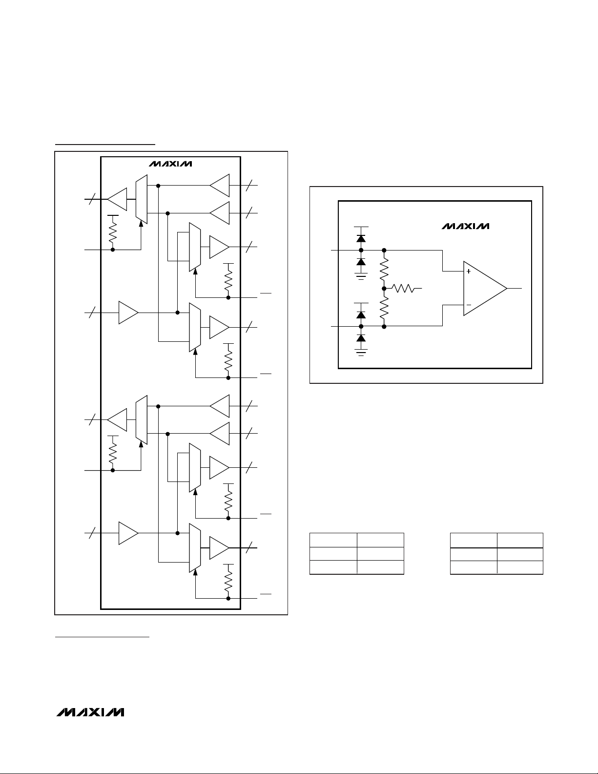
Detailed Description
The MAX3783 is a 2.7Gbps dual serial mux/buffer with
selectable line-side loopback for system test. Each half
of the MAX3783 provides a transmitter with a fanout of
two and a receiver with a 2:1 mux, as shown in the functional diagram.
Input Stages
The input amplifiers accept CML or AC-coupled PECL
signals and each input has an on-chip 100Ω differential
impedance for optimal termination, as shown in Figure 1.
Control Lines
TTL-compatible control lines are provided to select the
MAX3783’s operating mode (Table 1). SELA and SELB
set the mux for channels A and B, respectively, to
select LI1_ or LI2_ to connect to the SO_ output. LB1A,
LB1B, LB2A, and LB2B enable loopback mode for
each of the four LO_ outputs. All control lines are internally pulled high through 15kΩ resistors.
Output Buffers
The outputs are high-speed CML interfaces with 50Ω
back termination, as shown in Figure 2.
Exposed-Pad (EP) Package
The exposed pad on the 48-pin TQFP-EP provides a
very low thermal-resistance path for heat removal from
the IC. The pad is also electrical ground on the
MAX3783 and must be soldered to the circuit board for
proper thermal and electrical performance.
MAX3783
2.7Gbps Dual Mux/Buffer with Loopback
_______________________________________________________________________________________ 5
Figure 1. Input Structure
Functional Diagram
Table 1. Operating Modes
SOA
SELA
SOB
SELB
MAX3783
1
CML
2
V
CC
0
15kΩ
SIA
CML
2
1
CML
2
V
CC
0
15kΩ
CML
CML
1
CML
V
15kΩ
CML
15kΩ
CML
15kΩ
CML
CML
CC
V
CC
V
CC
0
1
0
1
0
LI1A
2
LI2A
2
LO2A
2
LB2A
LO1A
2
LB1A
LI1B
2
LI2B
2
LO2B
2
V
CC
MAX3783
IN+
50Ω
1.2kΩ
V
CC
IN-
50Ω
VCC - 0.5V
LB2B
SIB
CML
2
1
CML
V
0
CC
15kΩ
LO1B
2
LB1B
SEL_ SO_
0 LI2_
1 LI1_
LB_ LO_
0 LI_
1 SI_
Page 6

MAX3783
Chip Information
TRANSISTOR COUNT: 2816
PROCESS: BiPOLAR
2.7Gbps Dual Mux/Buffer with Loopback
6 _______________________________________________________________________________________
Figure 2. CML Output Structure
Package Information
(For the latest package outline information, go to
www.maxim-ic.com/packages
.)
PACKAGE TYPE DOCUMENT NO.
48 TQFP-EP
21-0065
V
CC
MAX3783
50Ω 50Ω
32mA
OUT+
OUT-
Page 7
MAX3783
2.7Gbps Dual Mux/Buffer with Loopback
_______________________________________________________________________________________ 7
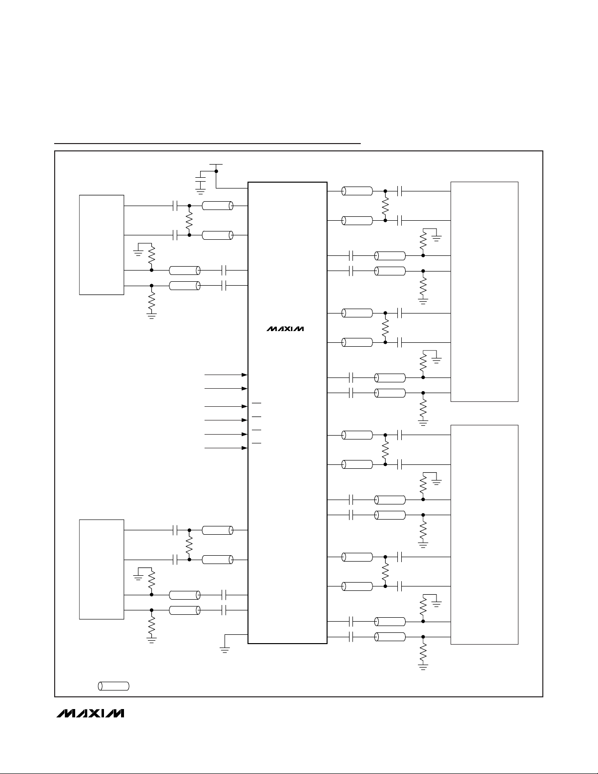
Typical Application Circuit
SERDES
A
OUT
V
CC
V
CC
SOA+
IN
SOA-
SIA+
SIA-
MAX3783
SELA
SELB
LB1A
LB2A
LB1B
LB2B
LO1A+
LO1A-
LI1A+
LI1A-
LO1B+
LO1B-
LI1B+
LI1B-
LO2A+
LO2A-
IN
OUT
IN
OUT
IN
SWITCH
1
SERDES
B
LI2A+
LI2A-
SOB+
IN
SOB-
OUT
NOTE: COUPLING CAPACITORS AND BIAS RESISTORS ARE OPTIONAL, SHOWN FOR LVPECL OPERATION.
REFER TO APPLICATION NOTES HFAN-01.0 AND HFAN-01.1 REGARDING LVPECL/CML INTERFACE.
THIS SYMBOL INDICATES A CONTROLLED-IMPEDANCE TRANSMISSION LINE OF CHARACTERISTIC IMPEDANCE Z
SIB+
SIB-
GND
LO2B+
LO2B-
LI2B+
LI2B-
= 50Ω.
0
OUT
IN
OUT
SWITCH
2
Page 8

MAX3783
2.7Gbps Dual Mux/Buffer with Loopback
Maxim cannot assume responsibility for use of any circuitry other than circuitry entirely embodied in a Maxim product. No circuit patent licenses are
implied. Maxim reserves the right to change the circuitry and specifications without notice at any time.
8
_____________________Maxim Integrated Products, 120 San Gabriel Drive, Sunnyvale, CA 94086 408-737-7600
© 2008 Maxim Integrated Products is a registered trademark of Maxim Integrated Products, Inc.
Revision History
REVISION
NUMBER
0 10/01 Initial release. —
1 3/06 Added lead-free device to the Ordering Information table. 1
2 1/08
REVISION
DATE
DESCRIPTION
In the Electrical Characteristics tab le, mod ified Note 2 and added Note 6 for t
t
; replaced package outl ine drawings with table.
F
PAGES
CHANGED
,
R
2, 8, 9
 Loading...