

________________General Description
The MAX3766 is a complete, easy-to-program laser
driver for fiber optic LAN transmitters, optimized for
operation at 622Mbps. It includes a laser modulator,
automatic power control (APC), and a failure indicator
with latched shutdown.
Laser modulation current can be programmed up to
60mA at 622Mbps. A programmable modulation temperature coefficient can be used to keep the transmitted extinction ratio nearly constant over a wide
temperature range. The modulator operates at data
rates up to 1.25Gbps at reduced modulation current.
APC circuitry uses feedback from the laser’s monitor
photodiode to adjust the laser bias current, producing
constant output power regardless of laser temperature
or age. The MAX3766 supports laser bias currents up
to 80mA.
The MAX3766 provides extensive laser safety features,
including a failure indicator with latched shutdown and
a smooth start-up bias generator. These features help
ensure that the transmitter output does not reach hazardous levels. The MAX3766 is available in a compact
20-pin QSOP and dice.
________________________Applications
622Mbps ATM Transmitters
1.25Gbps Fiber Optic LAN Transmitters
1.25Gbps Ethernet Transmitters
____________________________Features
♦ 60mA Modulation Current
♦ 80mA Bias Current
♦ 200ps Edge Speed
♦ Modulation-Current Temperature Compensation
♦ Automatic Power Control
♦ Laser-Fail Indicator with Latched Shutdown
♦ Smooth Laser Start-Up
MAX3766
622Mbps LAN/WAN Laser Driver with
Automatic Power Control and Safety Shutdown
________________________________________________________________
Maxim Integrated Products
1
19-1249; Rev 0b; 10/97
PART
MAX3766EEP
MAX3766E/D -40°C to +85°C
-40°C to +85°C
TEMP. RANGE PIN-PACKAGE
20 QSOP
Dice*
EVALUATION KIT
AVAILABLE
Ordering Information
*
Dice are designed to operate over this range, but are tested and
guaranteed at T
A
= +25°C only. Contact factory for availability.
Typical Application Circuits appear at end of data sheet.
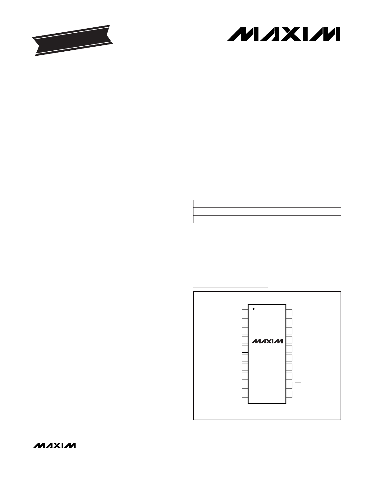
Pin Configuration
20
19
18
17
16
15
14
13
1
2
3
4
5
6
7
8
REF1
POWERSET
MD
GNDOUTMOD
REF2
TC
BIASMAX
TOP VIEW
BIAS
OUT+
OUTV
CCOUT
GND
IN+
IN-
GND
12
11
9
10
FAIL
SAFETYENABLE
V
CC
MAX3766
QSOP
For free samples & the latest literature: http://www.maxim-ic.com, or phone 1-800-998-8800.
For small orders, phone 408-737-7600 ext. 3468.

MAX3766
622Mbps LAN/WAN Laser Driver with
Automatic Power Control and Safety Shutdown
2 _______________________________________________________________________________________
ABSOLUTE MAXIMUM RATINGS
ELECTRICAL CHARACTERISTICS
Stresses beyond those listed under “Absolute Maximum Ratings” may cause permanent damage to the device. These are stress ratings only, and functional
operation of the device at these or any other conditions beyond those indicated in the operational sections of the specifications is not implied. Exposure to
absolute maximum rating conditions for extended periods may affect device reliability.
Supply Voltage, VCC, V
CC
OUT
.................................-0.5V to 7.0V
Voltage at IN+, IN-, ENABLE,
SAFETY,
FAIL ...........................................-0.5V to (VCC+ 0.5V)
Voltage at MOD, BIASMAX, POWERSET, TC..........-0.5V to 4.0V
Current out of REF1, REF2 .................................-0.1mA to 10mA
Current into OUT+, OUT- ....................................-5mA to 100mA
Current into BIAS.................................................-5mA to 130mA
Current into MD.......................................................-5mA to 5mA
Current into FAIL ...................................................-5mA to 30mA
Current into SAFETY..............................................-5mA to 10mA
Continuous Power Dissipation (T
A
= +85°C)
QSOP (derate 9.1mW/°C above +85°C).......................590mW
Operating Junction Temperature Range...........-40°C to +150°C
Processing Temperature (dice).......................................+400°C
Storage Temperature Range.............................-55°C to +150°C
Lead Temperature (soldering, 10sec).............................+300°C
CONDITIONS UNITSMIN TYP MAXPARAMETER
V4.5 5.0 5.5Supply Voltage, V
CC
(Note 1) °C-40 25 85Ambient Operating Temperature
Referenced to V
CC
V-1.4 -1.3 -1.19Input Common-Mode Voltage
V0.8Enable Input Low
V
IN+
- V
IN-
, common-mode input =
VCC- 1.3V, Figure 1
V2.0Enable Input High
mV500 1000 1800Differential Input Signal Amplitude
VVCC- 2.5Voltage at BIAS
While using APC %50Data Duty Cycle
GbpsDC to 1.25Data Rate
VVCC- 2.5Voltage at OUT+, OUT-
Not tested mA/mA0.001 to 0.1Laser to PIN Coupling
R
F AIL
= 5.1kΩ V4.3
FAIL Output High
(Note 3) mA0.5 80Bias-Current Range
ICC(Note 2)
IMD> 15µA, R
F AIL
= 5.1kΩ V0.33 0.44
FAIL Output Low
mA21 25 32Supply Current
µA0.1 10
Bias Current when Driver is
Disabled or Shut Down
Input data low (Note 2) µA1 200Modulation Current
Input data high (Note 3) mA2 60
Modulation-Current Programmable
Range
RTC= 0Ω ppm/°C-50
Minimum Modulation-Current
Temperature Compensation
µA10
Modulation Current when Driver is
Disabled or Shut Down
All DC testing uses 5.1kΩ load kΩ2.7 to 20
FAIL Load
RTC= open ppm/°C5600
Maximum Modulation-Current
Temperature Compensation
RECOMMENDED OPERATING CONDITIONS
DC PARAMETERS
MAX3766
622Mbps LAN/WAN Laser Driver with
Automatic Power Control and Safety Shutdown
_______________________________________________________________________________________ 3
ELECTRICAL CHARACTERISTICS (continued)
Note 1: Dice are tested at room temperature only (TA= +25°C).
Note 2: V
CC
= +5.5V, R
BIASMAX
= 887Ω, R
MOD
= 887Ω, R
POWERSET
= 287Ω, RTC= 0Ω, V
BIAS
= V
OUT+
= V
OUT-
= 3.0V. Supply
current excludes I
BIAS
, I
OUT+
, I
OUT-
, and I
FAIL
.
Note 3: Total output current must be reduced at high temperatures with packaged product to maintain maximum junction
temperature of T
j
= +150°C. See the
Design Procedure
section.
Note 4: All AC parameters are measured with a 25Ω load. I
MOD
is the AC current amplitude at either OUT pin. The AC voltage at
OUT is greater than V
CC
- 2.5V.
Note 5: Pulse-width distortion is measured at the 50% crossing point. Data input is a 155MHz square wave, with tR≈ 300ps.
Note 6: AC specifications are guaranteed by design and characterization.
V
CC
- V
MD
V1.5 2.1 2.3Monitor-Diode Bias Voltage
Referenced to V
CC
V-2.8Lower MD Voltage for Failure
Referenced to V
CC
V-1.2Upper MD Voltage for Failure
Referenced to nominal V
REF1
V0.5REF1 Voltage for Failure
TA= +25°C, V
REF2
V2.1 2.4 2.7REF2 Reference Voltage
Width of operating window, centered at
nominal V
MD
TA= +25°C, V
REF1
V
CONDITIONS
2.8 3.1 3.4REF1 Reference Voltage
mV300Range of MD for No Failure
I
MOD
= 60mA 210 400
Output Edge Speed (20% to 80%)
I
MOD
= 10mA
ps
125 250
I
MOD
= 30mA 160 300
I
MOD
= 30mA %10Output Aberrations
µA15 2000
Monitor-Diode Current
Programmable Range
UNITSMIN TYP MAXPARAMETER
I
MOD
= 60mA 5 80
I
MOD
= 30mA 20 80
I
MOD
= 10mA
ps
80 120
Pulse-Width Distortion
RMS, TA= +25°C, VCC= +5V, I
MOD
= 30mA ps2 3Random Jitter
AC PARAMETERS (Notes 4, 5, and 6)
MAX3766
622Mbps LAN/WAN Laser Driver with
Automatic Power Control and Safety Shutdown
4 _______________________________________________________________________________________
Typical Operating Characteristics
(Typical Operating Characteristics are measured on the MAX3766 evaluation kit, VCC= +5.0V, TA = +25°C, unless otherwise noted.)
0
20
10
30
40
-40 0
20
-20 40
60
80 100
SUPPLY CURRENT vs. TEMPERATURE
(EXCLUDES OUTPUT CURRENTS AND I
FAIL
)
MAX3766-01
AMBIENT TEMPERATURE (°C)
SUPPLY CURRENT (mA)
6000
4000
1 1k10 100 10k 100k 1M
MODULATION CURRENT TEMPCO
vs. R
TC
MAX3766-02
RTC (Ω)
TEMPCO (ppm/°C)
0
2000
100
1
1 1k10
100
10k
100k
DIE MODULATION CURRENT vs. R
MOD
(TJ = +25°C)
MAX3766-03
R
MOD
(Ω)
LASER MODULATION CURRENT (mAp-p)
10
TEMPCO = 0ppm/°C
TEMPCO = 5600ppm/°C
TEMPCO = 3000ppm/°C
100
1
1 1k10 100 10k 100k
MODULATION CURRENT vs. R
MOD
(20 QSOP, TA = +25°C)
MAX3766-04
R
MOD
(Ω)
LASER MODULATION CURRENT (mAp-p)
10
TEMPCO = 0ppm/°C
TEMPCO = 3000ppm/°C
TEMPCO = 5600ppm/°C
125µW/div
161ps/div
EYE DIAGRAM
(622Mbps, 1300nm LASER, 470MHz FILTER)
MAX3766-07
231- 1 PRBS
20
30
40
50
60
70
-40 0
20
-20 40
60
80 100
MODULATION CURRENT
vs. TEMPERATURE
MAX3766-05
AMBIENT TEMPERATURE (°C)
MODULATION CURRENT (mAp-p)
RTC = 100Ω
RTC = 330Ω
RTC = 1kΩ
RTC = 3.3kΩ
RTC = 10kΩ
RTC = 100kΩ
0
50
100
150
200
250
0 3010 20
40
50 60
MODULATION EDGE SPEED AND
PWD vs. AMPLITUDE
MAX3766-06
MODULATION CURRENT (mAp-p)
20% TO 80% EDGE SPEED (ps)
TA = +85°C
TA = +25°C
TA = -40°C
PULSE-WIDTH
DISTORTION (ps)
60mA/div
81ps/div
EYE DIAGRAM
(1.244Gbps, 25Ω LOAD, I
MOD
= 60mA)
MAX3766-08
231- 1 PRBS
0.01
10.1 10 100 1000
MONITOR CURRENT vs. R
POWERSET
MAX3766-09
R
POWERSET
(kΩ)
MD CURRENT (mA)
0.1
1
10
MAX3766
622Mbps LAN/WAN Laser Driver with
Automatic Power Control and Safety Shutdown
_______________________________________________________________________________________
5
100
1 1k10 100 10k 100k
BIAS CURRENT vs. R
BIASMAX
(NO APC, OPEN-LOOP CONFIGURATION)
MAX3766-10
R
BIASMAX
(Ω)
I
BIAS
(mA)
1
10
10
0.001
-40 -20 0 20 40 60 80 100
MONITOR CURRENT vs. TEMPERATURE
0.01
MAX3766-11
AMBIENT TEMPERATURE (°C)
I
MD
(mA)
0.1
1
NOMINAL = 1mA
NOMINAL = 200µA
NOMINAL = 20µA
NOMINAL = 2µA
100
260
240
220
200
180
160
140
120
DATA-DEPENDENT JITTER
vs. TEMPERATURE (CMD = 0.1µF)
MAX3766-12
AMBIENT TEMPERATURE (°C)
DDJ (ps)
-40 -20 0 20 40 60 80 100
2
13
PRBS PATTERN
72 CONSECUTIVE ZEROS
223- 1 PRBS PATTERN
10µs/div
UNSUCCESSFUL STARTUP
MAX3766-13
V
ENABLE
V
MD
V
SAFETY
(τ = 30µs)
FAIL
DATA OUT (AC COUPLED)
5µs/div
100µW/
div
ABRUPT SHUTDOWN
MAX3766-16
OPTICAL OUTPUT WITH DATA ON
OPTICAL OUTPUT WITH DATA OFF
50µs/div
SUCCESSFUL STARTUP
MAX3766-14
V
ENABLE
V
MD
FAIL
V
SAFETY
(τ = 1500µs)
DATA OUT (AC COUPLED)
5µs/div
100µW/
div
SMOOTH STARTUP
MAX3766-15
OPTICAL OUTPUT WITH DATA ON
OPTICAL OUTPUT WITH DATA OFF
2.00
2.80
2.60
2.40
2.20
3.20
3.00
3.40
-45 -5
20
-25 40
60
80 100
REFERENCE VOLTAGE
vs. TEMPERATURE
MAX3766-17
AMBIENT TEMPERATURE (°C)
VOLTAGE (V)
RTC = OPEN
V
REF1
V
REF2
Typical Operating Characteristics (continued)
(Typical Operating Characteristics are measured on the MAX3766 evaluation kit, VCC= +5.0V, TA = +25°C, unless otherwise noted.)

MAX3766
622Mbps LAN/WAN Laser Driver with
Automatic Power Control and Safety Shutdown
6 _______________________________________________________________________________________
Pin Description
ENABLE is a TTL-compatible input. When low or open, this pin disables the output modulation and bias
current.
ENABLE10
A capacitor to ground at SAFETY determines the turn-on delay for the safety circuits. If SAFETY is
grounded or TTL low, internal safety shutdown features are disabled. A TTL high at SAFETY enables the
internal safety shutdown features.
SAFETY11
The FAIL output asserts low if the voltage at MD is above or below nominal. FAIL also asserts if REF1 is
inadvertently tied to the positive supply. FAIL has TTL-compatible output voltage levels.
FAIL
12
Supply Voltage for the Output Current DriversV
CCOUT
13
Inverting Modulation-Current OutputOUT-14
Ground. All grounds must be connected.GND5, 8
Inverting Data InputIN-6
Noninverting Data InputIN+7
Positive Supply Voltage. All VCCpins must be connected.V
CC
9
The current into MOD programs the laser modulation current. Connect MOD to REF2 with a resistor or
potentiometer.
MOD4
REF2 is the reference voltage used to program the modulation current. The tempco of REF2 is programmed by RTC.
REF23
PIN
The resistance (RTC) between TC and REF1 programs the temperature coefficient of REF2. Connecting
TC directly to REF1 produces the minimum tempco. Leaving TC unconnected produces the maximum
tempco.
TC2
The current into BIASMAX sets the maximum laser bias current. Connecting BIASMAX directly to REF1
allows the largest possible bias current.
BIASMAX1
FUNCTIONNAME
Ground for the Output Current DriversGNDOUT17
Input for the laser monitor photodiode current. MD18
The current into POWERSET programs the average optical output power when automatic power
control is used.
POWERSET19
REF1 is a voltage reference used to program laser bias current and average power.REF120
Noninverting Modulation-Current OutputOUT+15
Connection for the DC Laser Bias CurrentBIAS16

MAX3766
622Mbps LAN/WAN Laser Driver with
Automatic Power Control and Safety Shutdown
_______________________________________________________________________________________ 7
_______________Detailed Description
Figure 2 is a functional block diagram of the MAX3766
laser driver. The major functional blocks are the reference generator, PECL input buffer, laser-bias circuit,
modulation-current driver, automatic power control
(APC), failure detection, and safety circuit.
Reference Generator
The MAX3766 provides adjustments for maximum
laser-bias current, laser modulation current, and average laser power. To program these adjustments, simply
use the currents obtained by inserting a resistor in
series with integrated voltage references REF1 and
REF2. The temperature coefficient (tempco) of REF1
compensates for the tempco of the bias, modulation,
and APC current mirrors. Therefore, a programming
current derived from REF1 is constant with temperature. REF2 provides a positive tempco, which can be
applied to the modulation current. A positive modulation-current tempco will compensate for the thermal
characteristics of typical laser diodes. The modulationcurrent tempco is programmed by an external resistor
(RTC), which is connected from REF1 to TC. RTCand
an internal 2kΩ resistor form a weighted sum of the
temperature-compensated reference (REF1) and the
temperature-increasing reference, which is buffered
and output at REF2. REF1 and REF2 are stable with no
bypass capacitance. Bypass filtering REF1 or REF2 is
not required.
PECL Input Buffer
The differential PECL input signals are connected to the
high-speed PECL input buffer at IN+ and IN-. The input
impedance at IN+ and IN- is greater than 100kΩ, and
the input bias current is less than 10µA. The
MAX3766’s data inputs are not self-biasing. The common-mode input should be set by the external PECL
termination circuitry. To obtain good AC performance,
inputs should always be greater than 2.2V and less
than VCC.
Laser Modulation-Current Driver
The laser modulation-current driver consists of a current mirror and an emitter coupled pair. The mirror has
a gain of +30mA/mA. Modulation-current amplitude is
programmed with external resistor R
MOD
connected
from REF2 to MOD. R
MOD
can be estimated as follows:
with RTC= 0Ω.
The MAX3766 AC output drives up to 60mA of laser
current. Pulse-width distortion and overshoot are lowest
between 30mA and 60mA. However, output edge
speed increases at lower currents. When the output
current is between 2mA and 60mA, the edge speed is
suitable for communications up to 622Mbps. Edge
speeds below 30mA are suitable for communications up
to 1.25Gbps (see
Typical Operating Characteristics
).
The modulation-current tempco can be programmed
with an external resistor RTC, as described in the
Reference Generator
section. An internal 520Ω resistor
is included to limit the maximum modulation current if
MOD is connected directly to REF2.
If the MAX3766 is shut down or disabled, the modulation programming current is shunted to ground. Any
remaining modulation current is switched to OUT-.
For optimum performance, the voltage at OUT+ and
OUT- must always exceed VCC- 2.5V.
Laser Bias Circuit
The laser bias circuit is a current mirror with a gain of
+40mA/mA. Redundant controls disable the bias current
during a shutdown or disable event: the programming
current is switched off, and any remaining bias output
current is switched away from the laser. Ensure that the
voltage at BIAS always remains above VCC- 2.5V. If the
bias circuit is not used, connect BIAS to VCC.
R =
1.55V 30
I
MOD
MOD
( )
− 520Ω
V
IN+
VOLTS
250mV MIN
900mV MAX
500mV MIN
1800mV MAX
500mV MIN
1800mV MAX
I
MOD
I
OUT+
TIME
V
IN-
V
IN-
V
IN+
- V
IN-
V
IN+
RESULTING SIGNAL
SINGLE-ENDED INPUT
DIFFERENTIAL INPUT
Figure 1. Required Input Signal and Output Polarity

MAX3766
The available laser bias current is programmed by
connecting external resistor R
BIASMAX
from REF1 to
BIASMAX. The BIASMAX programming current is
adjusted by the APC circuit and amplified by the laser
bias circuit.
An internal 520Ω resistor between BIASMAX and the
mirror input at internal node APC limits the maximum
laser bias current when BIASMAX is connected directly
to REF1. BIASMAX can be directly connected to REF1
in space-constrained designs, causing the maximum
programming current (about 2.5mA) to flow into
BIASMAX. Selecting a BIASMAX resistor saves power
and limits the transmitter’s maximum light output.
R
BIASMAX
can be estimated as follows:
This equation applies to maximum bias currents above
10mA.
R =
1.55V 40
I
520
BIASMAX
BIASMAX
( )
− Ω
622Mbps LAN/WAN Laser Driver with
Automatic Power Control and Safety Shutdown
8 _______________________________________________________________________________________
SAFETY
START-UP
CIRCUIT
FAILURE
DETECTION
REFERENCE
GENERATOR
2k
V
V
TEMP
BANDGAP
POWERSET
MIRROR
1X
AUTOMATIC
POWER CONTROL
V
CC
- 2V
MONITORDIODE
AMPLIFIER
LASER BIAS CIRCUIT
BIAS
MIRROR
40X
APC
I
LBP
I
BIASMAX
I
APC
TEMP
MODULATION
MIRROR
30X
PECL
INPUT
BUFFER
ENABLE
SHDN
SAFETY
V
CC
V
CC
FAIL MOD REF2 TC REF1 BIASMAX
C
MD
V
CC
V
CC
V
CC
MONITOR
PHOTODIODE
LASER
MD
BIAS
OUT+
OUT-
POWERSET
R
POWERSET
R
BIASMAX
R
TC
R
MOD
5.1k
520Ω
520Ω 300Ω
FAILURE
SHDN
GNDOUT VCCOUT
V
CC
IN+
IN-
MODULATIONCURRENT
DRIVER
MAX3766
Figure 2. Functional Diagram

Automatic Power Control
Transmitters employing a laser with monitor photodiode
can use the APC circuit to maintain constant power,
regardless of laser threshold changes due to temperature
and aging. The APC circuit consists of the POWERSET
current mirror and the monitor diode amplifier.
The POWERSET current mirror provides an accurate
method of programming the back facet monitor photodiode current, which is assumed to be proportional to
laser output power. An external resistor from REF1 to
POWERSET programs the current in the unity-gain current mirror. R
POWERSET
can be estimated as follows:
The monitor-diode amplifier senses the current from the
monitor photodiode at MD, provides gain, and adjusts
the laser bias programming current (I
LBP
). The monitordiode amplifier forces the monitor-diode current to
equal the current programmed at POWERSET. The
monitor-diode amplifier can reduce the laser bias programming current, but cannot increase it. Therefore,
the APC circuit can adjust laser bias current between 0
and the setting determined by R
BIASMAX
.
When the APC feedback loop is closed, the voltage at
MD is approximately 2V below VCC. If the loop cannot
close due to excess or insufficient photocurrent, a failure is detected by the failure-detection circuit. Internal
circuitry prevents the voltage at MD from dropping
below VCC- 3.2V.
The stability and time constant of the APC feedback
loop is determined by an external compensation
capacitor (CMD) of at least 0.1µF. Connect the compensation capacitor from VCCto MD, as shown in
Typical Application Circuits
, to ensure a smooth start-
up at power-on or transmitter enable.
If a monitor diode is not available, the APC feature can
be disabled by connecting R
POWERSET
to GND and
leaving MD unconnected.
Failure Detection
Figure 3 shows a simplified schematic of the failuredetection circuit. The failure-detection circuit senses
two conditions. First, if the APC control loop cannot
control the monitor current due to laser undercurrent,
overcurrent, or a fault condition, a window comparator
detects that VMDis above or below VCC- 2V and
asserts the failure signal. Second, if REF1 is shorted to
the positive supply (or any another voltage above the
normal operating level), a comparator detects this condition and asserts the failure signal. If left undetected,
the reference voltage would rise, the current at POWERSET would increase, and the APC loop would attempt to
add laser current beyond the intended value.
Either failure condition causes the FAIL output to assert
TTL low. The FAIL output buffer is an open-collector
output and is designed to operate with a 5.1kΩ external
pull-up resistor.
Safety/Start-Up Circuit
The safety circuit includes the digital logic needed to
provide a latched internal shutdown signal (SHDN) for
disabling the laser if a failure condition exists. The
MAX3766 produces less than 20µA of total laser current when disabled by safety features or by the
ENABLE input. Figure 4 is a simplified schematic of the
safety circuit.
If ENABLE is low or open, the laser bias and modulation outputs are disabled by SHDN, regardless of the
state of the safety logic. The TTL-compatible ENABLE
input is internally pulled low with a 100kΩ resistor.
There are two useful safety configurations: failure
indication and latched shutdown.
Failure-Indication Configuration
Select the failure-indication configuration by connecting
SAFETY to ground. In this configuration, a failure condition is reported at FAIL, but does not cause a latched
shutdown. This configuration requires no additional circuitry for start-up.
R =
1.55V
I
POWERSET
MOD
− 300Ω
MAX3766
622Mbps LAN/WAN Laser Driver with
Automatic Power Control and Safety Shutdown
_______________________________________________________________________________________ 9
V
MD
FAILURE
(INTERNAL)
200mV
200mV
2V
V
CC
0.5V
V
REF1
V
BANDGAP
Figure 3. Failure-Detection Circuit (Simplified)

MAX3766
Latched Shutdown Configuration
This configuration is shown in the
Typical Application
Circuits
(configured for best performance), and can
be selected by connecting a capacitor (C
SAFETY
) to
ground at SAFETY. In this configuration, the transmitter
is shut down when a failure is detected. It can be
restarted only by a power-on cycle or a toggle of the
ENABLE input.
During start-up, FAIL is asserted until laser power reaches the programmed level. The safety circuit must be disabled at power-on or at transmitter enable, providing
enough time for the APC circuit to reach the programmed
laser power level.
In space-constrained designs, C
SAFETY
can be selected to provide a shutdown delay. When power is initially
applied, or when the ENABLE signal is toggled from a
logic 0 to a logic 1, the voltage at SAFETY is low, and
rises with a time constant set by C
SAFETY
and an internal 200kΩ pull-up resistor. The SAFETY signal is inverted and resets the input of a reset-dominant RS flip-flop.
The internal signal FAILURE from the failure-detection
circuit is connected to the set input of the flip-flop. After
SAFETY has gone high (allowing time for the APC feedback loop to settle) and if internal signal FAILURE is low,
the flip-flop output is low, and the bias and modulation
outputs are allowed to remain on. Refer to Figure 5 for
a timing diagram of start-up in the latched shutdown
configuration.
The duration of t
SAFETY
must be about 10 times t
APC
for
a successful start-up. After start-up, the transmitter
operates normally until a failure is detected, causing
the output currents to be shut down. The laser-current
outputs remain off until the failure condition is eliminated and the ENABLE input is toggled, or until the power
is cycled. A potential problem with this transmitterenable method is that a slow-rising power supply may
not enable the transmitter.
622Mbps LAN/WAN Laser Driver with
Automatic Power Control and Safety Shutdown
10 ______________________________________________________________________________________
S
RESET DOMINATE
RS FLIP-FLOP
OPEN
COLLECTOR
FAIL
Q
ENABLE
C
SAFETY
SAFETY
OPEN
COLLECTOR
100k
200k
V
CC
FAILURE
(INTERNAL)
SHDN
(INTERNAL)
SIMPLIFIED
OPEN-COLLECTOR
OUTPUT CIRCUIT
OUT
IN
R
Figure 4. Simplified Safety Circuit Schematic
V
CC
VCC ON (OR ENABLE SWITCHED TO ON STATE)
LASER BIAS AND
MODULATION CURRENT
t
ON
t
APC
t
SAFETY
OUTPUT CURRENTS ENABLED AFTER A FIXED DELAY
FAIL DEASSERTS WHEN THE APC LOOP SETTLES
SAFETY FEATURES START CHECKING
THE FAILURE SIGNAL AFTER A TIME SET
BY A CAPACITOR ON THE SAFETY INPUT.
AFTER THIS TIME, THE LASER DRIVER IS
DISABLED IF A FAILURE OCCURS.
FAIL
OUTPUT
SAFETY
Figure 5. Start-Up Sequence Timing

If PC board space is not a constraint, Maxim recommends enabling the transmitter with a reset-pulse generator, such as the MAX809, which generates a reset
signal after VCCreaches 4.5V (Figure 6). This method
ensures that the transmitter starts correctly, even if the
supply ramps very slowly.
__________________Design Procedure
Select Laser
Select a communications-grade laser with a rise time of
0.5ns or better for 622Mbps applications. The voltage
swing at the OUT+ pin affects the output waveform,
and is largely determined by the laser resistance,
inductance, and modulation current. To obtain the
MAX3766’s AC specifications, the output voltage at
OUT+ must remain above VCC- 2.5V at all times.
An approximation for the minimum voltage at OUT+ is
given by the following equation (Table 1):
Select a laser that meets the output voltage criteria. A
high-efficiency laser requires low modulation current
and generates low voltage swing at OUT+. Laser package inductance can be reduced by trimming leads.
Typical package leads have inductance of 25nH per
inch (1nH/mm). A compensation filter network can also
be used to reduce ringing, edge speed, and voltage
swing.
V = V - V - I
OUT(MIN) CC(MIN) LASER MOD
( )
+ +
R R
L
t
L D
r
MAX3766
622Mbps LAN/WAN Laser Driver with
Automatic Power Control and Safety Shutdown
______________________________________________________________________________________ 11
MAX3766*
MAX809MEUR-T
SAFETY
C
SAFETY
RESET
V
CC
V
CC
OR
ENABLE
ENABLE
*IN LATCHED SHUTDOWN
CONFIGURATION
Figure 6. Reset Pulse Generator
Table 1. Output Voltage Approximation
Minimum power supplyV
CC(MIN)
4.5V
Laser dynamic resistanceR
L
3Ω
Laser forward voltage at operating powerV
LASER
1.3V
Any damping resistance or line termination in series with the laser
(but not in series with BIAS)
R
D
10Ω
20% to 80% rise time of the laser modulation current, filtered by a
compensation network
t
r
300ps
(20% to 80%)
Total series inductance of laser, laser package, and board traces to the
MAX3766
L 6nH
Laser modulation currentI
OUT
30mA
VARIABLE
Approximation for the lowest voltage at the OUT+ pinV
OUT(MIN)
DESCRIPTION TYPICAL VALUE
2.2V

MAX3766
Set Modulation-Current Tempco
Compute the required modulation tempco from the
slope efficiency of the laser at TA= +25°C and at a hot
temperature. Then select the value of RTCfrom the
Typical Operating Characteristics
.
For example, suppose a laser has a slope efficiency
(SE) of 0.021mW/mA at +25°C, which reduces to
0.018mW/mA at +85°C. The temperature coefficient is
given by the following:
From the
Typical Operating Characteristics
, the value
for RTC, which offsets the tempco of the laser, is 3kΩ. If
modulation temperature compensation is not desired,
connect TC directly to REF1.
Set Modulation Current
The modulation-current amplitude can be programmed
with a fixed resistor or adjusted with a potentiometer. A
small internal resistance is provided to prevent damage
if the potentiometer is adjusted to the end of its range.
The value of R
MOD
can be selected from the
Typical
Operating Characteristics
.
Example: A transmitter requires average power of
-8dBm (160µW), with an extinction ratio of 15. The optical signal output is 280µW (see
Optical Power
Relations
). If the slope efficiency is 0.021mW/mA at
+25°C, then the required modulation current is
0.280mW / 0.021mW/mA = 13.3mA. From the
Typical
Operating Characteristics
, the value of R
MOD
is select-
ed to be 3kΩ.
Set Average Laser Power
and Maximum Bias Current
When APC is used, the average power control is programmed by R
POWERSET
, which is typically a poten-
tiometer. The value of R
POWERSET
can be estimated
from the
Typical Operating Characteristics
.
Example: Suppose a transmitter’s output power will be
adjusted to -8dBm (160µW) average power during
manufacturing. The coupling efficiency from laser to
monitor photodiode varies from 0.4A/W to 0.8A/W for
the selected laser, causing monitor current to vary
between 64µA and 128µA. From the
Typical Operating
Characteristics
, R
POWERSET
should be adjustable
between 12kΩ and 24kΩ.
Select R
BIASMAX
to provide sufficient current for a hot
laser at its end of life. For example, if the expected
laser threshold at +85°C and end of life is 40mA, then
from the
Typical Operating Characteristics
, R
BIASMAX
should be 1kΩ or less.
If APC is not used, the laser bias current is pro-
grammed by R
BIASMAX
. Select R
BIASMAX
from the
Typical Operating Characteristics
.
Set APC Time Constant
Capacitor CMDdetermines the APC time constant, and
must be large enough not to cause data-dependent jitter. For 622Mbps SONET/ATM applications, Maxim recommends selecting CMD≥ 0.1µF.
Select C
SAFETY
When using the latched shutdown configuration, determine the minimum value of C
SAFETY
from the
Typical
Operating Characteristics
. Calculate C
SAFETY
as follows:
For example: If CMDis 0.1µF and typical monitor current (IMD) is 100µA, then the value of C
SAFETY
should
be 50nF or larger. This ensures that t
SAFETY
is at least
10 times the t
APC
.
Design Bias Filter
To reduce data-dependent jitter, add a filter at BIAS
(see
Typical Operating Circuit).
Maxim recommends a
1µH inductor or ferrite bead with a self-resonance frequency of 200MHz or more.
Design Laser-Compensation
Filter Network
Laser package lead inductance causes the laser
impedance to increase at high frequencies, which
leads to ringing, overshoot, and degradation of the output eye. A laser-compensation filter network can be
used to reduce the output load seen by the MAX3766
at high frequencies, thereby reducing output ringing
and overshoot.
The compensation components (R
COMP
and C
COMP
)
are most easily determined by experimentation. Begin
with a no-compensation network, and observe the ring
frequency (fn) of the laser and laser driver (Figure 7).
Begin with R
COMP
= 25Ω and C
COMP
= 1/(2πfnR
COMP
).
Increase C
COMP
until the desired transmitter eye is
obtained.
C
SAFETY
=•
C
20k I
MD
MD
Ω
Laser tempco
SE SE
SE 85 25
10
85 25
25
6
=
−
( )
• −
( )
•
= − °2380ppm C/
622Mbps LAN/WAN Laser Driver with
Automatic Power Control and Safety Shutdown
12 ______________________________________________________________________________________

Calculate Power Consumption
The MAX3766’s junction temperature must be kept
below +150°C at all times. Calculate total power dissipated on the MAX3766 by laser power as follows:
Power = VCC(ICC+ I
BIAS
+ I
MOD
)
- (I
MOD
/ 2 + I
BIAS
) V
LASER
.
where I
BIAS
is the maximum bias current allowed by
R
BIASMAX
, I
MOD
is the AC modulation current, V
LASER
is the typical laser forward voltage.
Junction temperature = power (Watts) • 110 (°C/W).
__________Applications Information
Optical Power Relations
Many MAX3766 specifications relate to output current
amplitude. When working with fiber optic transmitters,
the output is normally expressed in terms of average
optical power and extinction ratio (Figure 8). Table 2
lists relations that are helpful in converting optical
power to output signal amplitude when designing with
the MAX3766. The relations are true if the average duty
cycle of the input data is 50%.
Input Terminations
The MAX3766’s data inputs must be biased externally.
Refer to Figure 9 for common input terminations.
Laser Safety and IEC 825
The International Electrotechnical Commission (IEC)
determines standards for hazardous light emissions
from fiber optic transmitters. Specification IEC 825
defines the maximum light output for various hazard
levels. The MAX3766 provides features that aid compliance with IEC 825.
A common safety requirement is single-point fault tolerance, whereby one unplanned short, open, or resistive
connection does not cause excess light output. When
the MAX3766 is used in the latched shutdown configuration, as shown in
Typical Application Circuits
, the cir-
cuit responds as shown in Table 3.
Using the MAX3766 laser driver alone does not ensure
that a transmitter design is compliant with IEC 825. The
entire transmitter circuit and component selections must
be considered. Each customer must determine the level
of fault tolerance required by their application, recognizing that Maxim products are not designed or authorized
for use as components in systems intended for surgical
implant into the body, for applications intended to support or sustain life, or for any other application where the
failure of a Maxim product could create a situation
where personal injury or death may occur.
MAX3766
622Mbps LAN/WAN Laser Driver with
Automatic Power Control and Safety Shutdown
______________________________________________________________________________________ 13
500ps/div
CORRECTLY COMPENSATED
UNCOMPENSATED
OVERCOMPENSATED
Figure 7. Example Laser Compensation
TIME
P0
P1
OPTICAL
POWER
P
AVE
Figure 8. Optical Power Relations
SYMBOL RELATION
Average
Power
P
AVE
Extinction
Ratio
r
e
PARAMETER
Optical Power
of a “1”
P1
Optical Power
of a “0”
P0
Signal
Amplitude
P
INPUT
Table 2. Optical Power Definitions
P = P0 + P1
( )
AVE
r = 1 / P0
P
e
r
P P
1 21=
P P r
0 2 1= +
P P1 - P0 2P
INPUT AVE
e
AVE
r
+
e
/
( )
AVE e
= =
/2
r -1
e
r 1
e
+

MAX3766
622Mbps LAN/WAN Laser Driver with
Automatic Power Control and Safety Shutdown
14 ______________________________________________________________________________________
Table 3. MAX3766 Fault Response in Latched Shutdown Configuration
High voltage on REF1 causes a failure and latched
shutdown.
REF1
Normal condition for circuit operation.ENABLE
Modulation current is increased. Either the APC
circuit will reduce power levels, or an overcurrent
will be detected at MD, causing a failure signal
and latched shutdown.
REF2, TC, MOD
Normal condition for circuit operation.SAFETY
Normal condition for circuit operation.OUT-
No effect on circuit.
FAIL
Forces output to either constant 1 or 0. APC maintains the power level at the programmed level.
IN+, IN-
PIN
Depending upon the setting of R
POWERSET
,
there is either no effect, or a latched shutdown.
BIASMAX
CIRCUIT RESPONSE TO OVERVOLTAGE
OR SHORT TO V
CC
Modulation and bias currents are reduced or off;
no hazard exists.
Modulation and bias currents are shut down.
Modulation current is reduced; no hazard exists.
Safety shutdown features are disabled, but a
hazard is not created.
Forces output to be logic 1. APC maintains the
power level at the programmed level.
No effect on circuit.
Forces output to either constant 1 or 0. APC maintains the power level at the programmed level.
Bias current reduction causes a low laser output,
resulting in a latched shutdown.
CIRCUIT RESPONSE TO UNDERVOLTAGE
OR SHORT TO GROUND
Voltage increase at these pins will turn off the
laser.
OUT+, BIAS
High laser output asserts FAIL. A complete short
will destroy the laser, eliminating the hazard. A
resistive short may cause a hazard. External
circuitry combined with the FAIL signal may be
used to protect against a resistive short (Figure 10).
Laser output increases, but is limited by the setting
of R
BIASMAX
.
POWERSET Laser output decreases.
Voltage increase at MD causes a failure and output
current shutdown.
MD
Voltage decrease at MD causes a failure and
output current shutdown.

MAX3766
622Mbps LAN/WAN Laser Driver with
Automatic Power Control and Safety Shutdown
______________________________________________________________________________________ 15
Layout Considerations
The MAX3766 is a high-frequency product. The performance of the circuit is largely dependent upon the layout of the circuit board.
Use a multilayer circuit board with a dedicated ground
plane. Use short laser package leads placed close to
OUT+ and OUT- to keep output inductance low. Power
supplies should be capacitively bypassed to the
ground plane with surface-mount capacitors placed
near the power-supply pins.
Solutions to Common Problems
1) Laser output is ringing and contains overshoot.
This is often caused by inductive laser packaging.
Try reducing the lead length of the laser pins. Modify
the compensation network to reduce the driver’s output edge speed (see
Design Procedure
). This problem can also occur if the voltage at OUT+, OUT-, or
BIAS is below VCC- 2.5V. Test this by increasing the
supply voltage, or reducing the modulation current.
2) Low-frequency oscillation on the bias-current
output.
Ensure C
MD
≥ 0.1µF.
3) Modulation driver is not needed.
If only the bias-current driver and safety circuits are
needed, connect IN+ to VCC, and leave IN- unconnected. Connect OUT+ and OUT- to the supply.
Leave MOD, TC, and REF2 unconnected.
4) APC is not needed.
If only the high-speed modulation driver is used,
connect BIAS to VCC, and leave POWERSET, MD,
FAIL, and BIASMAX unconnected. Connect SAFETY
to ground.
5) Laser edge switching speed is low.
Refer to the
Design Bias Filter
section. It may be
necessary to select L
BIAS
with a higher self-resonat-
ing frequency.
Wire Bonding Die
The MAX3766 uses bondpads with gold metalization.
Make connections to the die with gold wire only, using
ball bonding techniques. Wedge bonding is not recommended. Pad size is 4 mils (0.1mm) square. Die thickness is typically 15 mils (0.38mm).
Interface Models
Figure 11 shows typical models for the inputs and outputs of the MAX3766, including package parasitics. If
dice are used, replace the package parasitic elements
with bondwire parasitic elements.
PECL
OUTPUT
IN
V
CC
- 2V
V
CC
V
CC
50Ω
68Ω
R2
2.87k
R3
11.8k
R1
10kΩ
180Ω
SINGLE-ENDED TERMINATION IS SHOWN. THE OTHER INPUT SHOULD BE
TERMINATED SIMILARLY, OR CONNECTED TO V
CC
- 1.3V.
MAX3766
RF OR NON-
PECL OUTPUT
IN
MAX3766
TTL OR
CMOS OUTPUT
IN
MAX3766
Figure 9. Input Terminations
FAIL
V
CC
V
CC
RESET
FAIL
OUT+
5.1k
5.1k
100k
V
CC
LASER
MAX3766
Figure 10. External Laser Shutdown Circuit

MAX3766
622Mbps LAN/WAN Laser Driver with
Automatic Power Control and Safety Shutdown
16 ______________________________________________________________________________________
V
IN+
0.2pF
0.4pF
Q1
Q2
Q3
Q4
0.2pF
Q1, Q2 INPUT BIAS CURRENT ≅ 1µA
Q1, Q2 INPUT RESISTANCE ≅ 1MΩ
Q3, Q4 OUTPUT RESISTANCE ≅ 100kΩ
Q5 OUTPUT RESISTANCE ≅ 100kΩ
0.4pF
250Ω
V
CC
1.5nH
1.5nH
V
CC
V
CC
1.5nH
1.5nH
1.5nH
0.2pF
0.2pF
1pF
1pF
0.2pF
2pF
Q5
I
BIAS
I
MOD
OUT+ OUT-
PACKAGE
PACKAGE
V
CC
- 2.5 VCC - 2.5
V
CC
- 2.5
INPUT
OUTPUT BIAS
V
IN-
250Ω
V
CC
V
CC
V
CC
PACKAGE
Figure 11. Interface Models

MAX3766
622Mbps LAN/WAN Laser Driver with
Automatic Power Control and Safety Shutdown
______________________________________________________________________________________ 17
V
CCOUT
CONFIGURED FOR MINIMUM COMPONENT COUNT.
FAILURE-INDICATION CONFIGURATION
LATCHED SHUTDOWN CONFIGURATION
CONFIGURED FOR BEST PERFORMANCE.
R
TC
SETS THE TEMPERATURE COEFFICIENT OF THE MODULATION CURRENT.
V
CC
REF2
IN+
IN-
BIASMAX
R
POWERSET
POWERSET
REF1
TC MOD
ENABLE
R
MOD
OUT-
V
CC
0.01µF
V
CC
C
MD
OUT+
BIAS
R
FAIL
5.1k
V
CC
FAIL
SAFETY
GNDOUT
GND
MD
V
CCOUT
V
CC
V
CC
ENABLE
REF2
IN+
IN-
BIASMAX
R
POWERSET
R
TC
POWERSET
REF1
TC MOD
R
MOD
OUT-
V
CC
C
MD
R
OUT-
R
D
C
COMP
V
CC
LASER
L
BIAS
R
COMP
R
FAIL
5.1k
OUT+
BIAS
FAIL
SAFETY
C
SAFETY
(OPTIONAL—SEE TEXT)
GNDOUT
GND
MD
MAX3766
MAX3766
0.01µF
LASER
R
BIASMAX
Typical Application Circuits

MAX3766
622Mbps LAN/WAN Laser Driver with
Automatic Power Control and Safety Shutdown
18 ______________________________________________________________________________________
___________________Chip Topography
0.056"
(1.422mm)
0.045"
(1.143mm)
OUT- OUT+ BIAS GNDOUT
REF2
TC
BIASMAX
REF1
POWERSET
MD
IN+ IN- GND MOD
GND
V
CC
ENABLE
SAFETY
V
CCOUT
FAIL
TRANSISTOR COUNT: 725
SUBSTRATE CONNECTED TO GND AND GNDOUT.

MAX3766
622Mbps LAN/WAN Laser Driver with
Automatic Power Control and Safety Shutdown
______________________________________________________________________________________ 19
________________________________________________________Package Information
QSOP.EPS

Maxim makes no warranty, representation or guarantee regarding the suitability of its products for any particular purpose, nor does Maxim assume any liability arising out of the application or use of any product or circuit and specifically disclaims any and all liability, including without limitation consequential or
incidental damages. “Typical” parameters can and do vary in different applications. All operating parameters, including “typicals” must be validated for
each customer application by customer’s technical experts. Maxim products are not designed, intended or authorized for use as components in systems
intended for surgical implant into the body, or other applications intended to support or sustain life, or for any other application in which the failure of the
Maxim product could create a situation where personal injury or death may occur.
20
____________________Maxim Integrated Products, 120 San Gabriel Drive, Sunnyvale, CA 94086 408-737-7600
© 1997 Maxim Integrated Products Printed USA is a registered trademark of Maxim Integrated Products.
MAX3766
622Mbps LAN/WAN Laser Driver with
Automatic Power Control and Safety Shutdown
NOTES
 Loading...