Page 1
现货库存、技术资料、百科信息、热点资讯,精彩尽在鼎好!
V
CC
V
CC
C
AZ
CAZ1 CAZ2
V
CC
V
CC
C
IN
0.01µF
0.01µF
0.01µF
C
IN
0.01µF
TH SQUELCH
N.C.
100Ω
IN-
IN+
OUT+
R
TERM
R
TERM
R
L
100Ω
OUT-
MAX3266
MAX3267
MAX3264CUE
MAX3265CUE
MAX3265EUE
LOS
LOSS
OF
SIGNAL
LOS
N.C.
R
TH
LEVEL
N.C.
General Description
The 1.25Gbps MAX3264/MAX3268/MAX3768 and the
2.5Gbps MAX3265/MAX3269/MAX3765 limiting amplifiers are designed for Gigabit Ethernet and Fibre
Channel optical receiver systems. The amplifiers accept
a wide range of input voltages and provide constantlevel output voltages with controlled edge speeds.
Additional features include RMS power detectors with
programmable loss-of-signal (LOS) indication, an
optional squelch function that mutes the data output signal when the input voltage falls below a programmable
threshold, and excellent jitter performance.
The MAX3264/MAX3265/MAX3765 feature current-mode
logic (CML) data outputs that are tolerant of inductive
connectors and a 16-pin TSSOP package, making these
circuits ideal for GBIC receivers. The MAX3268/
MAX3269/MAX3768 feature standards-compliant positive-referenced emitter-coupled logic (PECL) data outputs and are available in a tiny 10-pin µMAX package
that is ideal for small-form-factor (SFF) receivers.
Applications
Gigabit Ethernet Optical Receivers
Fibre Channel Optical Receivers
System Interconnect
ATM Optical Receivers
Features
♦ +3.0V to +5.5V Supply Voltage
♦ Low Deterministic Jitter
14ps (MAX3264)
11ps (MAX3265/MAX3765)
♦ 150ps (max) Edge Speed (MAX3265/MAX3765)
300ps (max) Edge Speed (MAX3264)
♦ Programmable Signal-Detect Function
♦ Choice of CML or PECL Output Interface
♦ 10-Pin µMAX or 16-Pin TSSOP Package
MAX3264/MAX3265/MAX3268/MAX3269/MAX3765/MAX3768
+3.0V to +5.5V, 1.25Gbps/2.5Gbps
Limiting Amplifiers
________________________________________________________________ Maxim Integrated Products 1
19-1523; Rev 6, 5/04
+Denotes lead-free package.
*EP = Exposed paddle.
**Dice are designed to operate from 0°C to +70°C, but are tested
and guaranteed only at T
A
= +25°C.
Ordering Information
Selector Guide appears at end of data sheet.
Pin Configurations appear at end of data sheet.
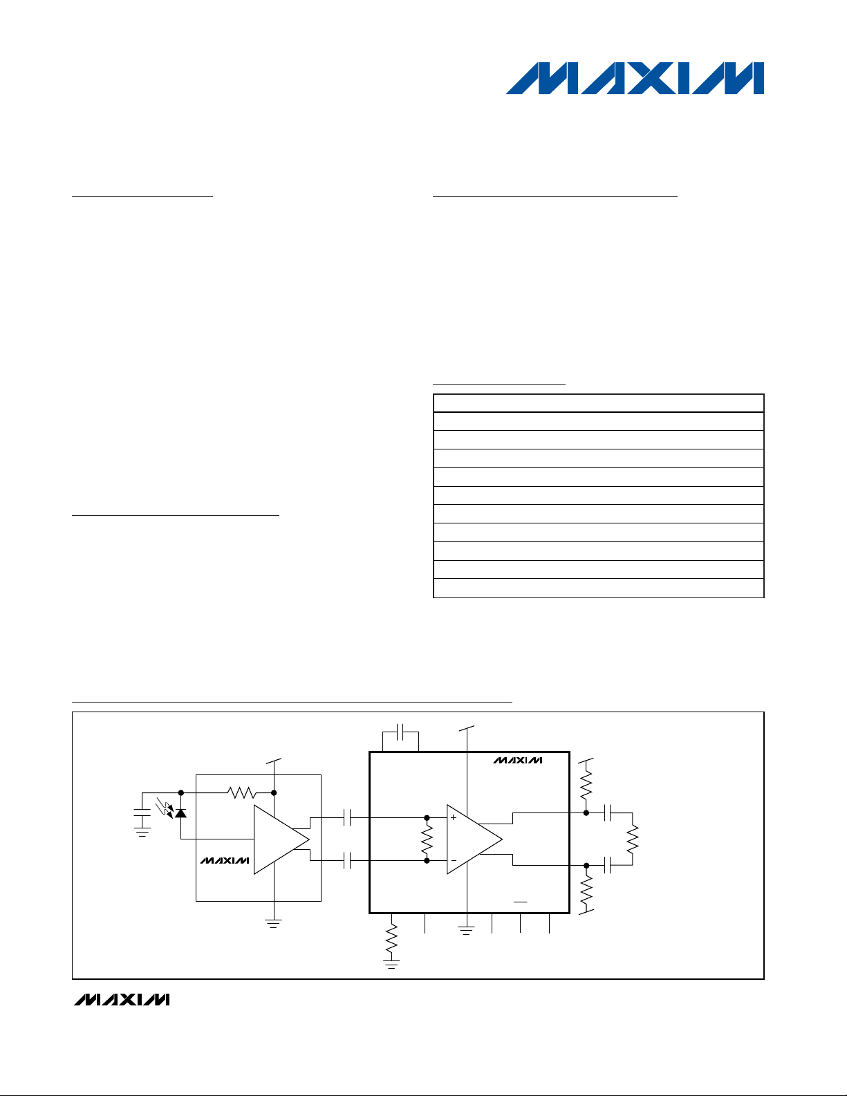
Typical Operating Circuits
Typical Operating Circuits continued at end of data sheet.
For pricing, delivery, and ordering information, please contact Maxim/Dallas Direct! at
1-888-629-4642, or visit Maxim’s website at www.maxim-ic.com.
PART TEMP RANGE
PIN-PACKAGE
MAX3264CUE 0°C to +70°C 16 TSSOP-EP*
MAX3264CUE+ 0°C to +70°C 16 TSSOP-EP*
MAX3264C/D 0°C to +70°C Dice**
MAX3265CUE 0°C to +70°C 16 TSSOP-EP*
MAX3265CUE+ 0°C to +70°C 16 TSSOP-EP*
MAX3265CUB 0°C to +70°C 10 µMAX-EP*
MAX3265CUB+ 0°C to +70°C 10 µMAX-EP*
MAX3265EUE -40°C to +85°C 16 TSSOP-EP*
MAX3265EUE+ -40°C to +85°C 16 TSSOP-EP*
MAX3265C/D 0°C to +70°C Dice**
Ordering Information continued at end of data sheet.
Page 2
MAX3264/MAX3265/MAX3268/MAX3269/MAX3765/MAX3768
+3.0V to +5.5V, 1.25Gbps/2.5Gbps
Limiting Amplifiers
2 _______________________________________________________________________________________
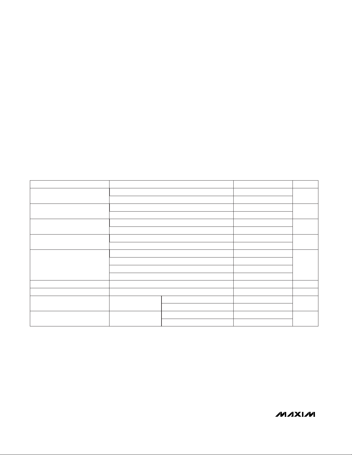
ABSOLUTE MAXIMUM RATINGS
ELECTRICAL CHARACTERISTICS
(Data outputs terminated per Figure 1, VCC= +3.0V to +5.5V, TA= 0°C to +70°C. Typical values are at V
CC
= +3.3V, TA= +25°C,
unless otherwise noted.) (Note 1)
Stresses beyond those listed under “Absolute Maximum Ratings” may cause permanent damage to the device. These are stress ratings only, and functional
operation of the device at these or any other conditions beyond those indicated in the operational sections of the specifications is not implied. Exposure to
absolute maximum rating conditions for extended periods may affect device reliability.
Supply Voltage (VCC)............................................-0.5V to +6.0V
Voltage at IN+, IN- ..........................(V
CC
- 2.4V) to (VCC+ 0.5V)
Voltage at SQUELCH, CAZ1,
CAZ2, LOS,
LOS, TH..................................-0.5V to (VCC+ 0.5V)
Voltage at LEVEL...................................................-0.5V to +2.0V
Current into LOS, LOS ..........................................-1mA to +9mA
Differential Input Voltage (IN+ - IN-) .....................................2.5V
Continuous Current at
CML Outputs (OUT+, OUT-)..........................-25mA to +25mA
Continuous Current at PECL Outputs (OUT+, OUT-) .........50mA
Continuous Power Dissipation (T
A
= +70°C)
16-Pin TSSOP (derate 27mW/°C above +70°C) .........2162mW
10-Pin µMAX (derate 20mW/°C above +70°C)...........1600mW
Operating Ambient Temperature Range.............-40°C to +85°C
Storage Temperature Range.............................-55°C to +150°C
Processing Temperature (dice).......................................+400°C
Lead Temperature (soldering, 10s).................................+300°C
Deterministic Jitter
MAX3265/MAX3269/MAX3765 (Notes 2, 3)
MAX3265/MAX3269/MAX3765
MAX3264/MAX3268/MAX3768
MAX3265/MAX3269/MAX3765
MAX3264/MAX3268/MAX3768
4.5
8.5
Low LOS Deassert Level mVRTH= 2.5kΩ
MAX3264/MAX3268/MAX3768 (Notes 2, 3)
PARAMETER MIN TYP MAX UNITS
10 1200
5 1200
Data Rate Gbps
Input Voltage Range mV
14 30
11 25
1.25
2.5
psp-p
15
Random Jitter
8
ps
RMS
80 175 300
100 150
80 150 300
Data Output Edge Speed
100 150
ps
LOS Hysteresis 2.5 4.4 dB
LOS Assert/Deassert Time 1 µs
1.20 2.6
2.20 4.8
Low LOS Assert Level mV
CONDITIONS
MAX3264/MAX3268/MAX3768 (Notes 2, 4)
MAX3265/MAX3269/MAX3765
MAX3264/MAX3268/MAX3768
MAX3265/MAX3269/MAX3765 (Notes 2, 4)
MAX3264 (Note 5)
MAX3265/MAX3765 (Note 6)
MAX3268/MAX3768 (Note 5)
MAX3269 (Note 6)
MAX3264/MAX3268/MAX3768
(Notes 2, 7)
MAX3265/MAX3269/MAX3765
(Notes 7, 8)
RTH= 2.5kΩ
Page 3
MAX3264/MAX3265/MAX3268/MAX3269/MAX3765/MAX3768
+3.0V to +5.5V, 1.25Gbps/2.5Gbps
Limiting Amplifiers
_______________________________________________________________________________________ 3
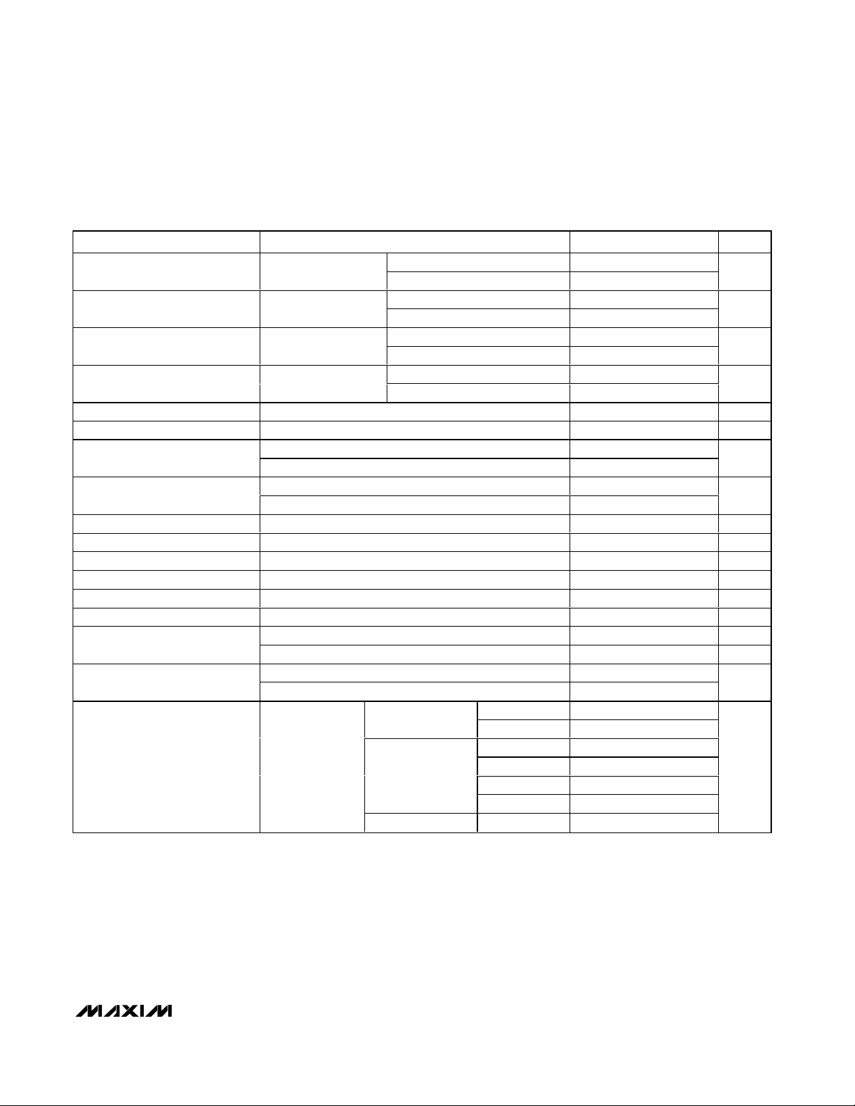
ELECTRICAL CHARACTERISTICS (continued)
(Data outputs terminated per Figure 1, VCC= +3.0V to +5.5V, TA= 0°C to +70°C. Typical values are at V
CC
= +3.3V, TA= +25°C,
unless otherwise noted.) (Note 1)
PARAMETER CONDITIONS
UNITS
MAX3264/MAX3268/MAX3768 5.6 9
Medium LOS Assert Level RTH = 7kΩ
MAX3265/MAX3269/MAX3765
9.9 16
mV
MAX3264/MAX3268/MAX3768
15
Medium LOS Deassert Level RTH = 7kΩ
MAX3265/MAX3269/MAX3765
27
mV
MAX3264/MAX3268/MAX3768 9.4
High LOS Assert Level RTH = 20kΩ
MAX3265/MAX3269/MAX3765
mV
MAX3264/MAX3268/MAX3768 35
High LOS Deassert Level RTH = 20kΩ
MAX3265/MAX3269/MAX3765 67
mV
Squelch Input Current 0 80 400 µA
Differential Input Resistance IN+ to IN- 97
103 Ω
MAX3264/MAX3268/MAX3768
Input-Referred Noise
MAX3265/MAX3269/MAX3765
µV
RMS
LEVEL = open, R
LOAD
= 50Ω
CML Output Voltage
LEVEL = GND, R
LOAD
= 75Ω
mV
PECL Output High Voltage
Referenced to V
CC
V
PECL Output Low Voltage
Referenced to V
CC
V
LOS Output High Voltage
I
LOS
= -30µA 2.4 V
LOS Output Low Voltage
I
LOS
= +1.2mA 0.4 V
Output Signal When Squelched
Outputs AC-coupled 20 mV
Power-Supply Rejection Ratio
f < 2MHz 20 dB
CAZ = open 2
MHz
Low-Frequency Cutoff
C
AZ
= 0.1µF 2 kHz
MAX3264/MAX3265/MAX3765 85
115
O utp ut Resi stance ( S i ng l e E nd ed )
MAX3268/MAX3269/MAX3768 4
Ω
MAX3268 39 62
MAX3269 48 78
MAX3264 38 62
MAX3265 50 76
MAX3765 50 76
Output not
squelched
MAX3768 39 62
Power-Supply Current Figure 2
MAX3765 64 90
mA
Output squelched
MIN TYP MAX
18.0 41.5
550 1200
1100 1270 1800
-1.025 -0.880
-1.810 +1.620
21.6
100
150
230
100
19.8
40.5
Page 4
mV
V
V
mV
MAX3264/MAX3265/MAX3268/MAX3269/MAX3765/MAX3768
+3.0V to +5.5V, 1.25Gbps/2.5Gbps
Limiting Amplifiers
4 _______________________________________________________________________________________
Note 1: Specifications for Input Voltage Range, LOS Assert/Deassert Levels, and CML Output Voltage refer to the total differential
peak-to-peak signal applied or measured. PECL output voltages are absolute (single-ended) voltages measured at a single
output.
Note 2: Input edge speed is controlled using four-pole, lowpass Bessel filters with bandwidth approximately 75% of the maximum
data rate.
Note 3: Deterministic jitter is measured with a K28.5 pattern (0011 1110 1011 0000 0101). Deterministic jitter is the peak-to-peak
deviation from ideal time crossings, measured at the zero-level crossings of the differential output per ANSI X3.230,
Annex A.
Note 4: Random jitter is measured with the minimum input signal applied after filtering with a four-pole, lowpass, Bessel filter (fre-
quency bandwidth at 75% of the maximum data rate). For Fibre Channel and Gigabit Ethernet applications, the peak-topeak random jitter is 14.1-times the RMS random jitter.
Note 5: Input signal applied after a 933MHz Bessel filter.
Note 6: Input signal applied after a 1.8GHz Bessel filter.
Note 7: Input for LOS assert/deassert and hysteresis tests is a repeating K28.5 pattern. Hysteresis is defined as:
20log (V
LOS-DEASSERT
/ V
LOS-ASSERT
).
Note 8: Response time to a 10dB change in input power.
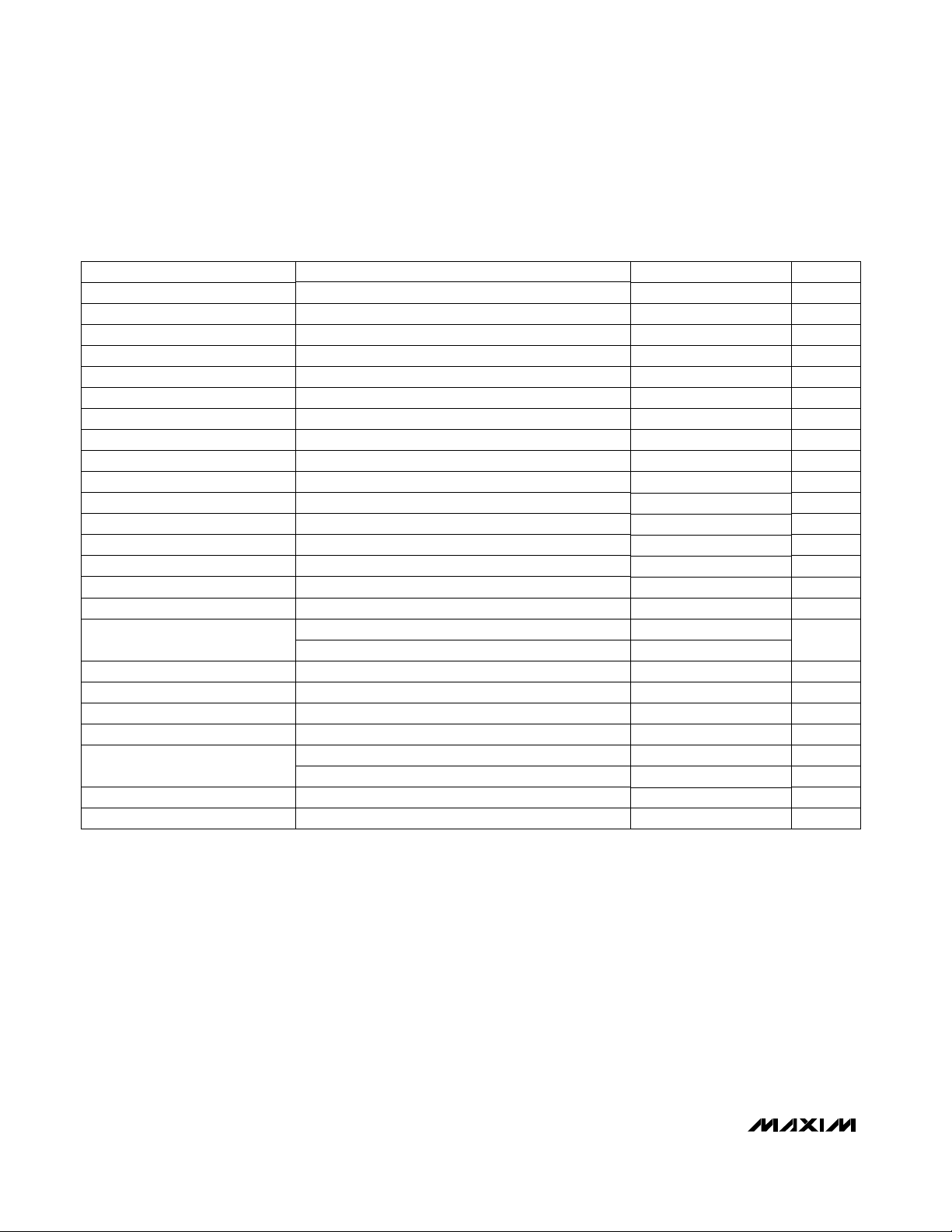
ELECTRICAL CHARACTERISTICS—MAX3265EUE
(Data outputs terminated per Figure 1, VCC= +3.0V to +5.5V, TA= -40°C to +85°C. Typical values are at V
CC
= +3.3V, TA= +25°C,
unless otherwise noted.) (Note 1)
CONDITIONS
Data Rate Gbps
2.5
UNITSMIN TYP MAXPARAMETER
Input Voltage Range mV
10 1200
(Notes 2, 3)Deterministic Jitter ps
p-p
11 25
(Notes 2, 4)Random Jitter ps
RMS
8
(Note 6)Data Output Edge Speed ps
100 155
(Notes 2, 7)LOS Hysteresis dB
2.2 4.4
(Notes 7, 8)LOS Assert/Deassert Time µs
1
Output Resistance (single ended) Ω
85 100 115
CAZ= 0.1µF kHz
2
CAZ= open
Low-Frequency Cutoff
MHz
2
f < 2MHzPower-Supply Rejection Ratio dB
20
Outputs AC-coupledOutput Signal When Squelched
20
I
LOS
= +1.2mALOS Output Low Voltage
0.450
I
LOS
= -30µALOS Output High Voltage
LEVEL = GND, R
LOAD
= 75Ω
1100 1270 1800
LEVEL = open, R
LOAD
= 50Ω
CML Output Voltage
550 1200
Input-Referred Noise
µV
RMS
230
IN+ to IN-Differential Input Resistance
Ω
97 100 103
Squelch Input Current
µA0 80 400
RTH= 20kΩHigh LOS Deassert Level mV
67 111
RTH= 20kΩHigh LOS Assert Level mV
18.0 41.5
RTH= 7kΩMedium LOS Deassert Level mV
27 43.0
RTH= 7kΩMedium LOS Assert Level mV
9.9 16
RTH= 2.5kΩLow LOS Deassert Level mV
8.5 13.6
RTH= 2.5kΩLow LOS Assert Level mV
2.20 4.8
Figure 2Power-Supply Current mA
50 76
2.4
Page 5
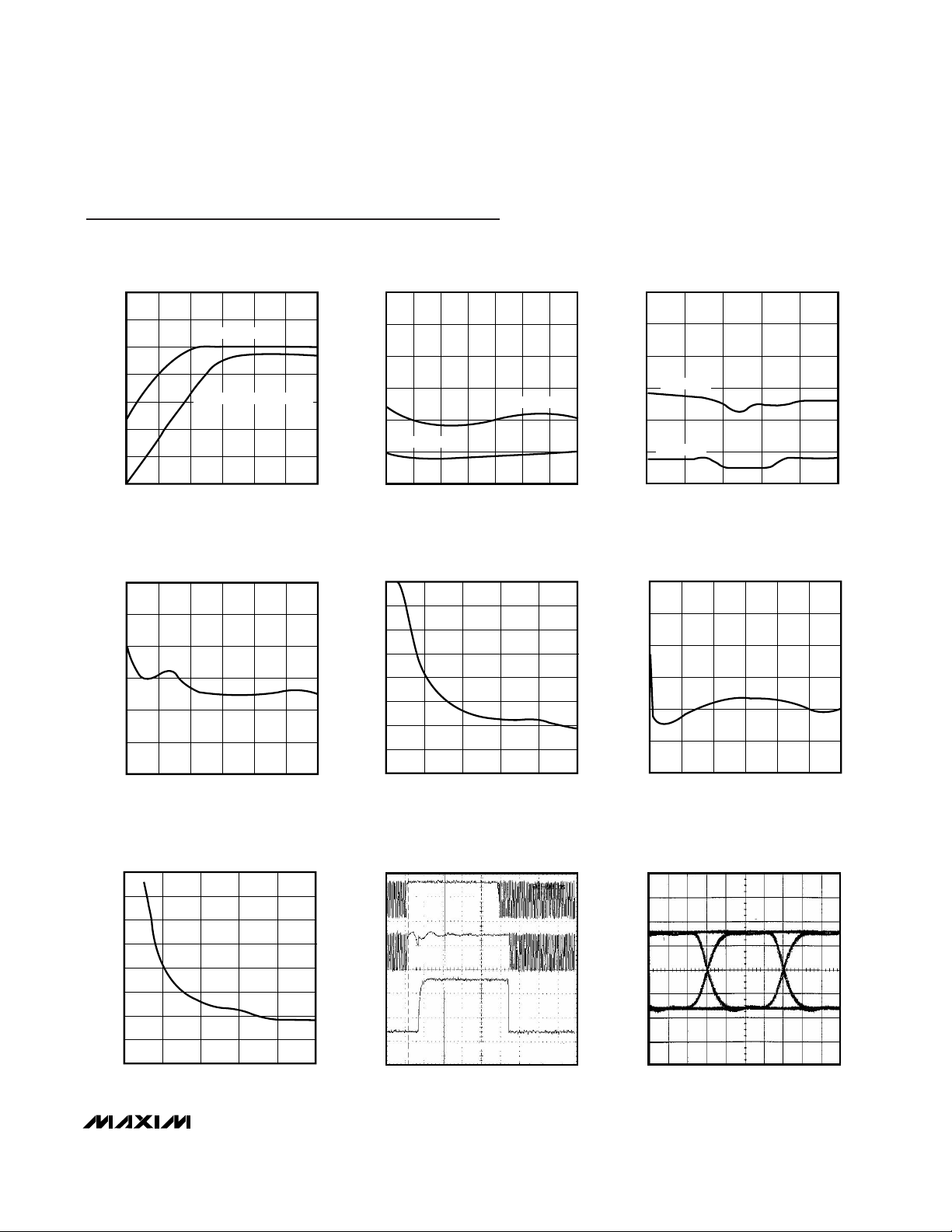
MAX3264/MAX3265/MAX3268/MAX3269/MAX3765/MAX3768
+3.0V to +5.5V, 1.25Gbps/2.5Gbps
Limiting Amplifiers
_______________________________________________________________________________________ 5
0
25
20
15
10
5
30
0 200 400 600 800 1000 1200
MAX3264/MAX3268/MAX3768
DETERMINISTIC JITTER
vs. INPUT AMPLITUDE
MAX3264/5/8/9 TOC04
INPUT AMPLITUDE (mV)
JITTER (ps)
0
14
12
10
8
6
2
4
16
0 1020304050
MAX3264/MAX3268/MAX3768
RANDOM JITTER
vs. INPUT AMPLITUDE
MAX3264/5/8/9 TOC05
INPUT AMPLITUDE (mV)
RMS JITTER (ps)
300
900
700
500
1300
1100
1500
1700
024681012
OUTPUT VOLTAGE
vs. INPUT VOLTAGE
MAX3264/5/8/9 TOC01a
INPUT VOLTAGE (mV)
OUTPUT VOLTAGE (mV)
MAX3264/MAX3268
MAX3265/MAX3269/MAX3765
3.5
4.0
6.5
6.0
5.5
5.0
4.5
0 10203040506070
MAX3264
LOS HYSTERESIS vs. TEMPERATURE
MAX3264/5/8/9 TOC03a
TEMPERATURE (°C)
LOS HYSTERESIS (dB)
RTH = 25kΩ
RTH = 7kΩ
0
25
20
15
10
5
30
0 200 400 600 800 1000 1200
MAX3265/MAX3269/MAX3765
DETERMINISTIC JITTER
vs. INPUT AMPLITUDE
MAX3264/5/8/9 TOC06
INPUT AMPLITUDE (mV)
JITTER (ps)
0
7
6
5
4
3
1
2
8
0 1020304050
MAX3265/MAX3269/MAX3765
RANDOM JITTER
vs. INPUT AMPLITUDE
MAX3264/5/8/9 TOC07
INPUT AMPLITUDE (mV)
RMS JITTER (ps)
V
IN
V
OUT
V
LOS
LOSS OF SIGNAL WITH SQUELCH
MAX3264/5/8/9 TOC08
500ns/div
300mV/div
200ps/div
MAX3268/MAX3768
DATA OUTPUT EYE DIAGRAM
(MINIMUM INPUT)
MAX3264/5/8/9 TOC09
Typical Operating Characteristics
(TA = +25°C, unless otherwise noted.)
3.5
4.0
6.5
6.0
5.5
5.0
4.5
-40 -15 10 35 60 85
MAX3265EUE
LOS HYSTERESIS vs. TEMPERATURE
MAX3264/5/8/9 TOC03
TEMPERATURE (°C)
LOS HYSTERESIS (dB)
RTH = 4.6kΩ
RTH = 16kΩ
Page 6
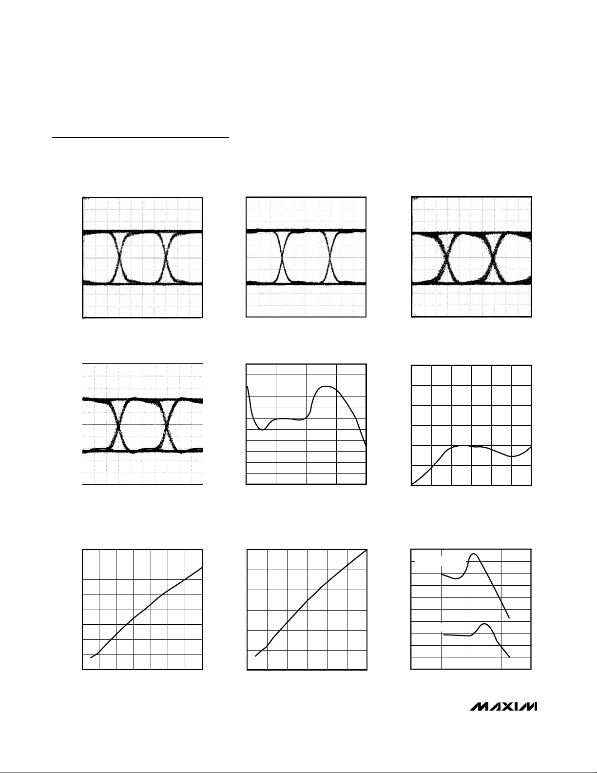
MAX3264/MAX3265/MAX3268/MAX3269/MAX3765/MAX3768
+3.0V to +5.5V, 1.25Gbps/2.5Gbps
Limiting Amplifiers
6 _______________________________________________________________________________________
Typical Operating Characteristics (continued)
(TA = +25°C, unless otherwise noted.)
150mV/div
MAX3265/MAX3765
DATA OUTPUT EYE DIAGRAM
2.5Gbps (MAXIMUM INPUT)
MAX3264/5/8/9 TOC13
100ps/div
0
25
15
20
10
5
100k 1M 10M 100M 1G
POWER-SUPPLY REJECTION RATIO
vs. FREQUENCY
MAX3264/5/8/9 TOC14
FREQUENCY (Hz)
PSRR (dB)
1.0
3.5
3.0
2.5
1.5
2.0
4.0
0 0.5 1.0 1.5 2.0 3.0
OUTPUT VSWR vs. FREQUENCY
MAX3264/5/8/9 TOC15
FREQUENCY (GHz)
VSWR
2.5
0
10
5
20
15
35
30
25
40
0105 1520253035
MAX3264
LOSS-OF-SIGNAL THRESHOLD vs. R
TH
MAX3264/5/8/9 TOC18
RTH (kΩ)
LOS ASSERT THRESHOLD (mV)
0
50
40
30
10
20
60
010203051525
MAX3265/MAX3765
LOSS-OF-SIGNAL THRESHOLD vs. R
TH
MAX3264/5/8/9 TOC19
RTH (kΩ)
LOS ASSERT THRESHOLD (mV)
5
40
45
50
35
30
20
15
10
25
55
1M 100M 10G10M 1G
COMMON-MODE REJECTION RATIO
vs. FREQUENCY
MAX3264/5/8/9 TOC20
FREQUENCY (Hz)
CMRR (dB)
MAX3268/MAX3768
MAX3265/MAX3765
150mV/div
MAX3264
DATA OUTPUT EYE DIAGRAM AT
1.25Gbps (MINIMUM INPUT)
MAX3264/5/8/9 TOC10
200ps/div
50mV/div
MAX3264
DATA OUTPUT EYE DIAGRAM AT
1.25Gbps (MAXIMUM INPUT)
MAX3264/5/8/9 TOC11
200ps/div
150mV/div
MAX3265/MAX3765
DATA OUTPUT EYE DIAGRAM
2.5Gbps (MINIMUM INPUT)
MAX3264/5/8/9 TOC12
100ps/div
Page 7

MAX3264/MAX3265/MAX3268/MAX3269/MAX3765/MAX3768
+3.0V to +5.5V, 1.25Gbps/2.5Gbps
Limiting Amplifiers
_______________________________________________________________________________________ 7
Pin Description
EP EP
Ground. The exposed paddle must be soldered to the circuit–board ground for
proper thermal performance.
Exposed
Paddle
— 7
Output Current Level. When this pin is not connected, the CML output current is
approximately 16mA. When this pin is connected to ground, the output current
increases to approximately 20mA. (In the MAX3265CUB/MAX3765CUB, LEVEL is
internally connected to ground.)
— 15
Squelch Input. The squelch function is disabled when SQUELCH is not connected
or is set to a TTL low level. When SQUELCH is set to a TTL high level and LOS is
asserted, the data outputs, OUT+, and OUT-, are forced to static levels. See sections PECL Output Buffer and CML Output Buffer for more information. (In the
MAX3265/MAX3268/MAX3269 10-pin µMAX, SQUELCH is not connected. In the
MAX3765/MAX3768, SQUELCH is internally connected to VCC.)
— 16 No ConnectionN.C.
SQUELCH
— 10
Noninverted Loss-of-Signal Output. LOS is low when the level of the input signal
is above the preset threshold set by the TH input. LOS asserts high when the signal level drops below the threshold.
LOS
LEVEL
— 1
Offset-Correction-Loop Capacitor. A capacitor connected between this pin and
CAZ2 extends the time constant of the offset correction loop.
— 2
Offset-Correction-Loop Capacitor. A capacitor connected between this pin and
CAZ1 extends the time constant of the offset correction loop. Refer to Design
Procedure.
CAZ2
CAZ1
6 9
Inverted Loss-of-Signal Output. LOS is high when the level of the input signal is
above the preset threshold set by the TH input. LOS is asserted low when the
signal level drops below the threshold.
8 12 Inverted Data Output
9 13 Noninverted Data OutputOUT+
OUT-
7, 10 11, 14 Supply VoltageV
CC
LOS
3 5 Inverted Input Signal
5 8
Loss-of-Signal Threshold. A resistor connected from this pin to ground sets the
input signal level at which the loss-of-signal (LOS) output(s) is asserted. Refer to
Typical Operating Characteristics and Design Procedure.
TH
IN-
2 4 Noninverted Input SignalIN+
TSSOP
FUNCTION
µMAX
NAME
GND1, 4 3, 6 Supply Ground
PIN
Page 8

MAX3264/MAX3265/MAX3268/MAX3269/MAX3765/MAX3768
+3.0V to +5.5V, 1.25Gbps/2.5Gbps
Limiting Amplifiers
8 _______________________________________________________________________________________
(a) MAX3264/MAX3265/MAX3765 WITH 50Ω TERMINATION
V
CC
100Ω 100Ω
100Ω
R
TERM
100Ω
2 x R
LOAD
100Ω
C
OUT
C
OUT
C
OUT
C
OUT
V
CC
(b) MAX3264/MAX3265/MAX3765 WITH 75Ω TERMINATION
V
CC
100Ω 100Ω
300Ω
R
TERM
300Ω
2 x R
LOAD
150Ω
V
CC
(c) MAX3268/MAX3269/MAX3768 OUTPUT TERMINATION
V
CC
V
CC
- 2V
OUTOUT+
50Ω
R
TERM
50Ω
MAX3264
MAX3265
MAX3765
MAX3264
MAX3265
MAX3765
MAX3268
MAX3269
MAX3768
Figure 1. Data Output Termination
Page 9

MAX3264/MAX3265/MAX3268/MAX3269/MAX3765/MAX3768
+3.0V to +5.5V, 1.25Gbps/2.5Gbps
Limiting Amplifiers
_______________________________________________________________________________________ 9
(a) CML SUPPLY CURRENT (ICC)
V
CC
I
CC
I
CC
V
CC
OUT+
OPEN
OPEN
OUT-
I
OUT
100Ω
R
TH
2.5kΩ
100Ω
CONTROL
SQUELCH
LEVEL
MAX3264CUE: OPEN
MAX3265CUE: OPEN
MAX3265CUB: GND (INTERNAL)
MAX3765CUB: V
CC
(INTERNAL)
(b) PECL SUPPLY CURRENT (ICC)
R
TH
2.5kΩ
MAX3264
MAX3265
MAX3765
MAX3268
MAX3269
MAX3768
MAX3264CUE: OPEN
MAX3265CUE: OPEN
MAX3265CUB: GND (INTERNAL)
MAX3765CUB: GND (INTERNAL)
Figure 2. Power-Supply Current Measurement
Page 10

MAX3264/MAX3265/MAX3268/MAX3269/MAX3765/MAX3768
+3.0V to +5.5V, 1.25Gbps/2.5Gbps
Limiting Amplifiers
10 ______________________________________________________________________________________
_______________Detailed Description
Figure 3 is a functional diagram of the MAX3264/
MAX3265/MAX3268/MAX3269/MAX3765/MAX3768 limiting amplifiers. A linear input buffer drives a multistage
limiting amplifier and an RMS power-detection circuit.
Offset correction with lowpass filtering ensures low
deterministic jitter. The output buffer produces a limited
output signal. The MAX3264/MAX3265/MAX3765 produce a CML output, while the MAX3268/MAX3269/
MAX3768 produce a PECL-compatible output signal.
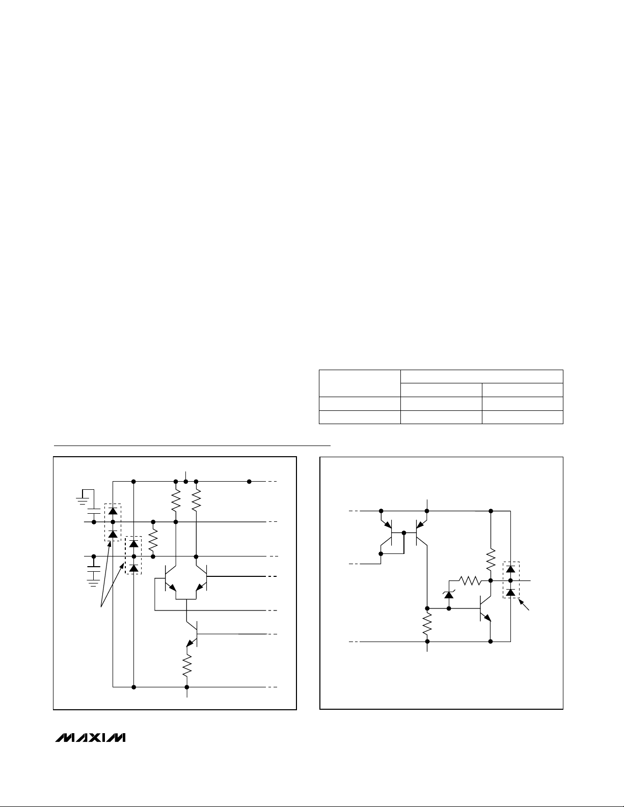
Schematics of these input/output circuits are shown in
Figures 4 through 7.
RMS Power Detect with
Loss-of-Signal Indicator
An RMS power detector looks at the signal from the
input buffer and compares it to a threshold set by the
TH resistor (see Typical Operating Characteristics for
appropriate resistor values). The signal-detect information is provided to the LOS outputs, which are internally
terminated with 8kΩ (MAX3265/MAX3269/MAX3765) or
16kΩ (MAX3264/MAX3268/MAX3768) pullup resistors.
The LOS outputs meet TTL voltage specifications when
loaded with a resistor ≥ 4.7kΩ.
CONTROL
GAIN
V
CC
TH
V
CC
R
LOS
= 8kΩ (MAX3265/MAX3269/MAX3765)
R
LOS
= 16kΩ (MAX3264/MAX3268/MAX3768)
LOS
R
LOS
R
LOS
LOS
OUT+
OUT-
SQUELCH
LEVEL
INPUT
BUFFER
CAZ1 CAZ2
OFFSET
CORRECTION
100Ω
IN+
IN-
MAX3264
MAX3265
MAX3268
MAX3269
MAX3765
MAX3768
LOWPASS
100pF
TOTAL GAIN = 55dB (MAX3264/MAX3268/MAX3768)
TOTAL GAIN = 49dB (MAX3265/MAX3269/MAX3765)
POWER DETECT
WITH
COMPARATOR
OUTPUT
BUFFER
TTL
TTL
Figure 3. Functional Diagram
Page 11
MAX3264/MAX3265/MAX3268/MAX3269/MAX3765/MAX3768
+3.0V to +5.5V, 1.25Gbps/2.5Gbps
Limiting Amplifiers
______________________________________________________________________________________ 11
Input Buffer
The input buffer is designed to accept input signals
from the MAX3266/MAX3267 transimpedance amplifiers. The input buffer provides a 100Ω input impedance between IN+ and IN-. Input VSWR is typically less
than 2.0 for frequencies less than 2GHz. DC-coupling
the inputs is not recommended; this prevents the DC
offset-correction circuitry from functioning properly.
Gain Stage and Offset Correction
The limiting amplifier provides approximately 55dB
(MAX3264/MAX3268/MAX3768) or 49dB (MAX3265/
MAX3269/MAX3765) of gain. This large gain makes the
amplifier susceptible to small DC offsets in the input signal. DC offsets as low as 1mV reduce the accuracy of
the power-detection circuit and may cause deterministic
jitter. A low-frequency feedback loop is integrated into
the limiting amplifier to reduce input offset, typically to
less than 100µV.
An external capacitor connected between CAZ1 and
CAZ2, in parallel with internal capacitance, determines
the time constant of the offset-correction circuit. The offset-correction circuit requires an average data-input
mark density of 50% to prevent an increase in dutycycle distortion and to ensure low deterministic jitter.
CML Output Buffer
The MAX3264/MAX3265/MAX3765 CML output circuits
(Figure 7) provide high tolerance to impedance mismatches and inductive connectors. The output current
can be set to two levels. When the LEVEL pin is left
unconnected, output current is approximately 16mA.
Connecting LEVEL to ground sets the output current to
approximately 20mA.
The squelch function is enabled when the SQUELCH pin
is set to a TTL-high level or connected to VCC. The
squelch function holds OUT+ and OUT- at a static voltage whenever the input signal power drops below the
loss-of-signal threshold. In the 10-pin µMAX package of
the MAX3265/MAX3268/MAX3269, the SQUELCH function is left internally unconnected. In the MAX3765/
MAX3768, the SQUELCH function is always enabled by
internally connecting it to VCC. SQUELCH operation for
the MAX3264/MAX3265 is described in Table 1.
Internal Input/Output Schematics
IN+
IN-
110Ω
GND
ESD
STRUCTURES
V
CC
500Ω
500Ω
0.25pF
0.25pF
Figure 4. Input Circuit
GND
R
T
= 8kΩ (MAX3265/MAX3269/MAX3765)
R
T
= 16kΩ (MAX3264/MAX3268/MAX3768)
ESD
STRUCTURE
V
CC
LOS
R
T
Figure 5. LOS Output Circuit
Table 1.
LEVEL PIN
VOLTAGE WHEN SQUELCHED
OUT- OUT+
Open VCC- 100mV V
CC
GND VCC- 100mV VCC- 100mV
Page 12

MAX3264/MAX3265/MAX3268/MAX3269/MAX3765/MAX3768
+3.0V to +5.5V, 1.25Gbps/2.5Gbps
Limiting Amplifiers
12 ______________________________________________________________________________________
The buffer’s output impedance is determined by the parallel combination of internal and external pullup resistors,
which are chosen to match the impedance of the transmission line (Figure 1). The output buffer can be AC- or
DC-coupled to the load.
PECL Output Buffer
The MAX3268/MAX3269/MAX3768 offer an industrystandard PECL output. The PECL outputs should be
terminated to VCC- 2V. Figure 6 shows the PECL output circuit. The squelch function forces OUT+ to a high
level and OUT- to a low level when the input is below
the programmed LOS threshold. In the 10-pin µMAX,
SQUELCH is left unconnected.
__________________Design Procedure
Program the LOS Assert Threshold
The loss-of-signal threshold is programmed by external
resistor RTH. See the LOS Threshold vs. RTHgraph in
the Typical Operating Characteristics.
Select the Coupling Capacitors
The coupling capacitors (C
IN, COUT
) should be select-
ed to minimize the receiver’s deterministic jitter. Jitter is
minimized when the input low-frequency cutoff (f
IN
) is
placed at a low frequency:
fIN= 1 / [2π(50)(C)]
For Fibre Channel, Gigabit Ethernet, or other applications using 8B/10B data coding, select (C
IN, COUT
) ≥
0.01µF, which provides fIN< 320kHz. For ATM/SONET
or other applications using scrambled NRZ data, select
(CIN,C
OUT
) ≥ 0.1µF, which provides fIN< 32kHz.
Select the Offset-Correction Capacitor
(MAX3264/MAX3265 TSSOP Only)
To maintain stability, it is important to keep a onedecade separation between fINand the low-frequency
cutoff (fOC) associated with the DC-offset-correction circuit.
fOC= 75 / [2π 60k (CAZ+ 100pF)]
= 200 x 10-6/ (C
AZ
+ 100pF)
For Fibre Channel, Gigabit Ethernet, or other applications using 8B/10B data coding, leave pins CAZ1, and
CAZ2 open (fOC= 2MHz). For ATM/SONET or other
applications using scrambled NRZ data, select C
AZ
≥
0.1µF, which typically provides f
OC
= 2kHz.
GND
ESD
STRUCTURES
V
CC
OUT-
OUT+
Figure 6. PECL Output Circuit
GND LEVEL
ESD
STRUCTURES
V
CC
100Ω 100Ω
OUT-
OUT+
Figure 7. CML Output Circuit
Page 13

MAX3264/MAX3265/MAX3268/MAX3269/MAX3765/MAX3768
+3.0V to +5.5V, 1.25Gbps/2.5Gbps
Limiting Amplifiers
______________________________________________________________________________________ 13
Applications Information
Optical Hysteresis
In an optical receiver, the electrical power change at
the limiting amplifier is 2x the optical power change.
As an example, if a receiver’s optical input power (x)
increases by a factor of two, and the preamplifier is linear, then the voltage input to the limiting amplifier also
increases by a factor of two.
The optical power change is 10log(2x / x) = 10log(2) =
+3dB.
At the limiting amplifier, the electrical power change is:
The MAX3264/MAX3265/MAX3268/MAX3269/MAX3765s’
typical voltage hysteresis is 4.4dB. This provides an optical hysteresis of 2.2dB.
GBIC Loss of Signal
In a GBIC application, the GBIC’s LOS output must be
high impedance when V
CC_
MODULE = GND. Figure 8
shows the recommended circuit to maintain high
impedance. ESD protection diodes on the MAX3264/
MAX3265/MAX3268/MAX3269/MAX3765/MAX3768
LOS outputs can be turned on when V
CC_
HOST >
V
CC_
MODULE.
PECL Terminations
The standard PECL termination (50Ω to VCC- 2V) is
recommended for best performance and output characteristics (see Figure 1). The data outputs operate at
high speed and should always drive transmission lines
with matched, balanced terminations.
Figure 9 shows an alternate method for terminating the
data outputs. The technique provides approximately
8mA DC bias current, with a 45Ω AC load, for the output termination. This technique is useful for viewing the
output on an oscilloscope or changing the PECL reference voltage.
Wire Bonding Dice
For high current density and reliable operation, the
MAX3264/MAX3265/MAX3268/MAX3269 use gold metalization. Make connections to the dice with gold wire
only, and use ballbonding techniques (wedge bonding
is not recommended). Die-pad size is 4-mils square,
with a 6-mil pitch. Die thickness is 15 mils (0.375mm).
10log
2V / R
V/ R
10log(2 ) 20log(2) 6dB
IN
2
IN
IN2IN
2
()
===+
V
CC_
MODULE
GBIC MODULE
V
CC_
HOST
4.7kΩ
HOST
LOS
GENERALPURPOSE
NPN
MAX3264
MAX3265
MAX3268
MAX3269
MAX3765
MAX3768
Figure 8. Recommended GBIC LOS Circuit
470Ω
DRIVING 50Ω TO GROUND
470Ω
50Ω
50Ω
OUT+
OUT-
MAX3268
MAX3269
MAX3768
Figure 9. Alternative PECL Termination
Page 14
MAX3264/MAX3265/MAX3268/MAX3269/MAX3765/MAX3768
+3.0V to +5.5V, 1.25Gbps/2.5Gbps
Limiting Amplifiers
14 ______________________________________________________________________________________
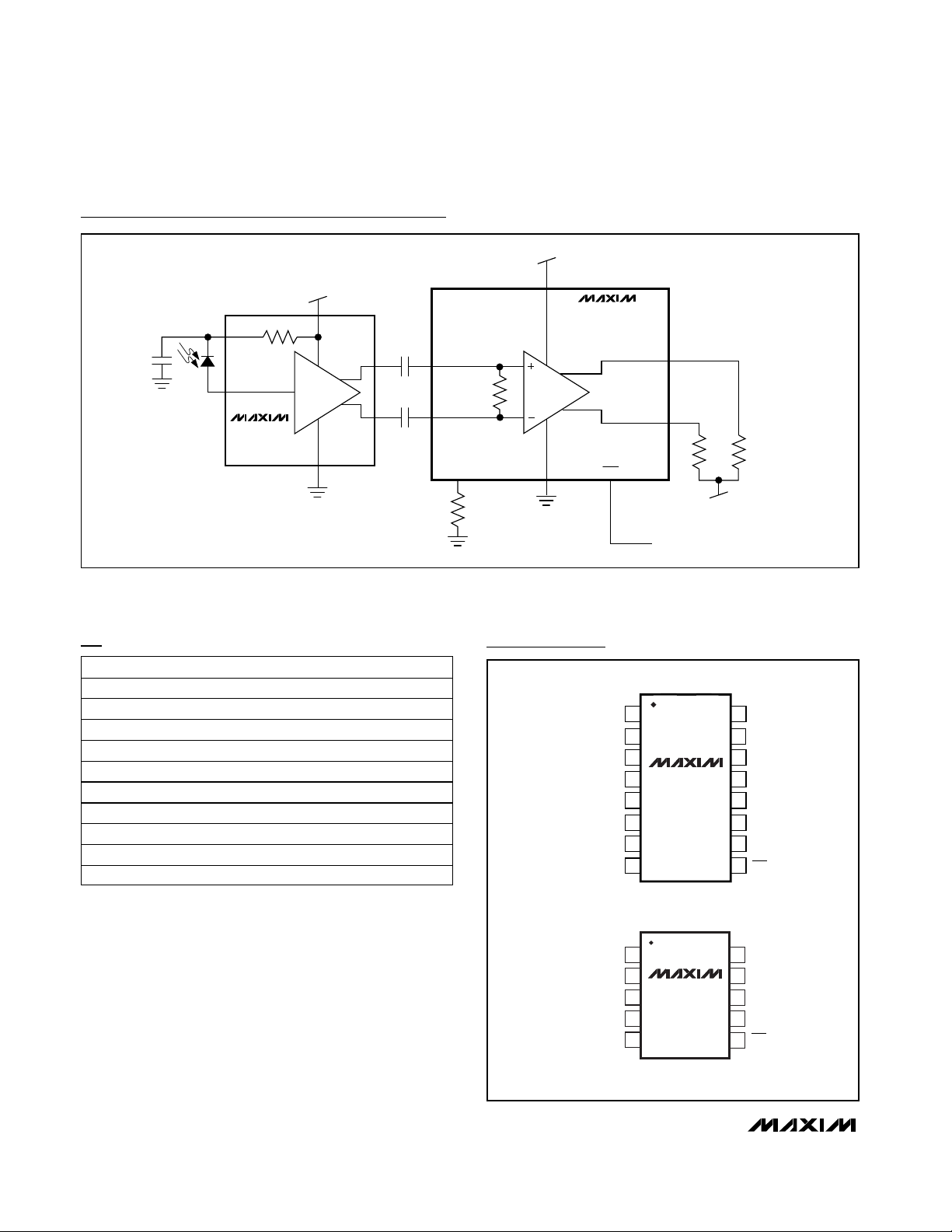
Typical Operating Circuits (continued)
50Ω 50Ω
R
TH
V
CC
V
CC
C
IN
0.01µF
C
IN
0.01µF
TH
100Ω
IN-
IN+
OUT+
OUT-
MAX3266
MAX3267
MAX3268CUB
MAX3269CUB
MAX3768CUB
LOS
SIGNAL DETECT
VCC - 2V
Pin Configurations
Ordering Information (continued)
PART TEMP RANGE
PIN-PACKAGE
MAX3268CUB 0°C to +70°C 10 µMAX-EP*
MAX3268CUB+ 0°C to +70°C 10 µMAX-EP*
MAX3268C/D 0°C to +70°C Dice**
MAX3269CUB 0°C to +70°C 10 µMAX-EP*
MAX3269CUB+ 0°C to +70°C 10 µMAX-EP*
MAX3269C/D 0°C to +70°C Dice**
MAX3765CUB 0°C to +70°C 10 µMAX-EP*
MAX3765CUB+ 0°C to +70°C 10 µMAX-EP*
MAX3768CUB 0°C to +70°C 10 µMAX-EP*
MAX3768CUB+ 0°C to +70°C 10 µMAX-EP*
+Denotes lead-free package.
*EP = Exposed paddle.
**Dice are designed to operate from 0°C to +70°C, but are tested
and guaranteed only at T
A
= +25°C.
TOP VIEW
1
CAZ1 N.C.
2
CAZ2
GND
3
MAX3264
4
IN+
IN-
GND
LEVEL
TH
MAX3265
5
6
7
8
16
15
14
13
12
11
10
9
SQUELCH
V
CC
OUT+
OUTV
CC
LOS
LOS
TSSOP
NOTE: EXPOSED PADDLE IS GROUND.
GND
1
IN+
IN-
GND
2
MAX3265
3
MAX3268
MAX3269
4
MAX3765
MAX3768
5
µMAX
10
V
CC
OUT+
9
OUT-
8
V
7
CC
LOSTH
6
Page 15

MAX3264/MAX3265/MAX3268/MAX3269/MAX3765/MAX3768
+3.0V to +5.5V, 1.25Gbps/2.5Gbps
Limiting Amplifiers
______________________________________________________________________________________ 15
Chip Topographies
IN-
GND
LEVEL
0.061"
(1.55mm)
0.061"
(1.55mm)
TH N.C.
LOS
SQUELCH
V
CC
OUT+
OUT-
V
CC
LOS
CAZ1
N.C.
IN+
CAZ2
GND
IN-
GND
0.061"
(1.55mm)
0.061"
(1.55mm)
TH N.C.
LOS
SQUELCH
V
CC
OUT+
OUT-
V
CC
LOS
CAZ1
N.C.
IN+
CAZ2
GND
MAX3264/MAX3265/MAX3765 MAX3268/MAX3269/MAX3768
MAX3264/MAX3265/MAX3765
TRANSISTOR COUNT: 726
MAX3268/MAX3269/MAX3768
TRANSISTOR COUNT: 728
SUBSTRATE CONNECTED TO GND
Selector Guide
*LEVEL pin grounded
CML
2.5MAX3765 10 µMAX-EP Enabled Maximum*
PECL 2.5MAX3269
CML 2.5MAX3265
1.25
1.25
DATA RATE
(Gbps)
10 µMAX-EP Disabled
10 µMAX-EP Disabled
Disabled
Selectable
Selectable
SQUELCH
FUNCTION
10 µMAX-EP
16 TSSOP-EP
16 TSSOP-EP
PIN-
PACKAGE
N/A
Maximum*
N/A
Selectable
Selectable
CML OUTPUT
LEVEL
PECLMAX3268
CMLMAX3264
OUTPUTPART
PECL 1.25MAX3768 10 µMAX-EP Enabled N/A
Page 16
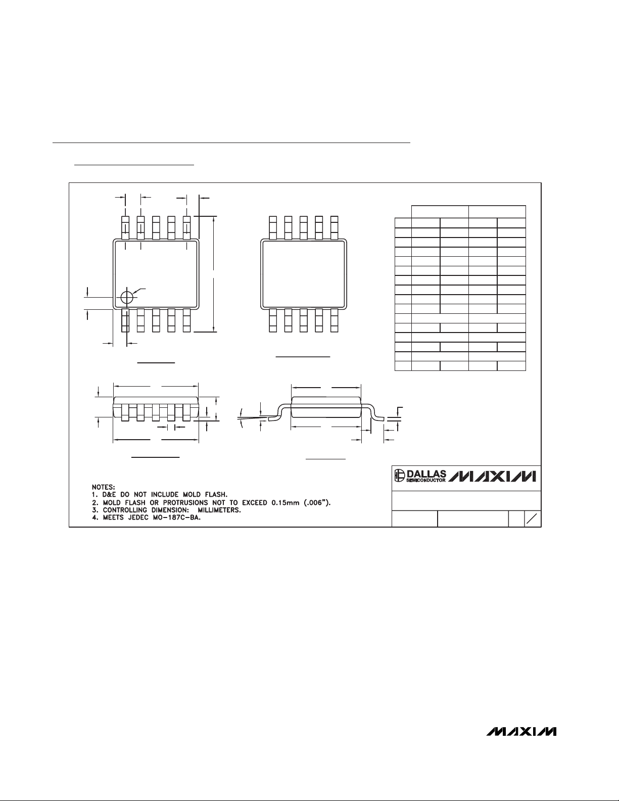
10LUMAX.EPS
PACKAGE OUTLINE, 10L uMAX/uSOP
1
1
21-0061
I
REV.DOCUMENT CONTROL NO.APPROVAL
PROPRIETARY INFORMATION
TITLE:
TOP VIEW
FRONT VIEW
1
0.498 REF
0.0196 REF
S
6°
SIDE VIEW
α
BOTTOM VIEW
0° 0° 6°
0.037 REF
0.0078
MAX
0.006
0.043
0.118
0.120
0.199
0.0275
0.118
0.0106
0.120
0.0197 BSC
INCHES
1
10
L1
0.0035
0.007
e
c
b
0.187
0.0157
0.114
H
L
E2
DIM
0.116
0.114
0.116
0.002
D2
E1
A1
D1
MIN
-A
0.940 REF
0.500 BSC
0.090
0.177
4.75
2.89
0.40
0.200
0.270
5.05
0.70
3.00
MILLIMETERS
0.05
2.89
2.95
2.95
-
MIN
3.00
3.05
0.15
3.05
MAX
1.10
10
0.6±0.1
0.6±0.1
0 0.50±0.1
H
4X S
e
D2
D1
b
A2
A
E2
E1
L
L1
c
α
GAGE PLANE
A2 0.030 0.037 0.75 0.95
A1
MAX3264/MAX3265/MAX3268/MAX3269/MAX3765/MAX3768
+3.0V to +5.5V, 1.25Gbps/2.5Gbps
Limiting Amplifiers
16 ______________________________________________________________________________________
Package Information
(The package drawing(s) in this data sheet may not reflect the most current specifications. For the latest package outline information,
go to www.maxim-ic.com/packages
.)
Page 17
Maxim cannot assume responsibility for use of any circuitry other than circuitry entirely embodied in a Maxim product. No circuit patent licenses are
implied. Maxim reserves the right to change the circuitry and specifications without notice at any time.
17 ____________________Maxim Integrated Products, 120 San Gabriel Drive, Sunnyvale, CA 94086 408-737-7600
© 2004 Maxim Integrated Products Printed USA is a registered trademark of Maxim Integrated Products.
MAX3264/MAX3265/MAX3268/MAX3269/MAX3765/MAX3768
+3.0V to +5.5V, 1.25Gbps/2.5Gbps
Limiting Amplifiers
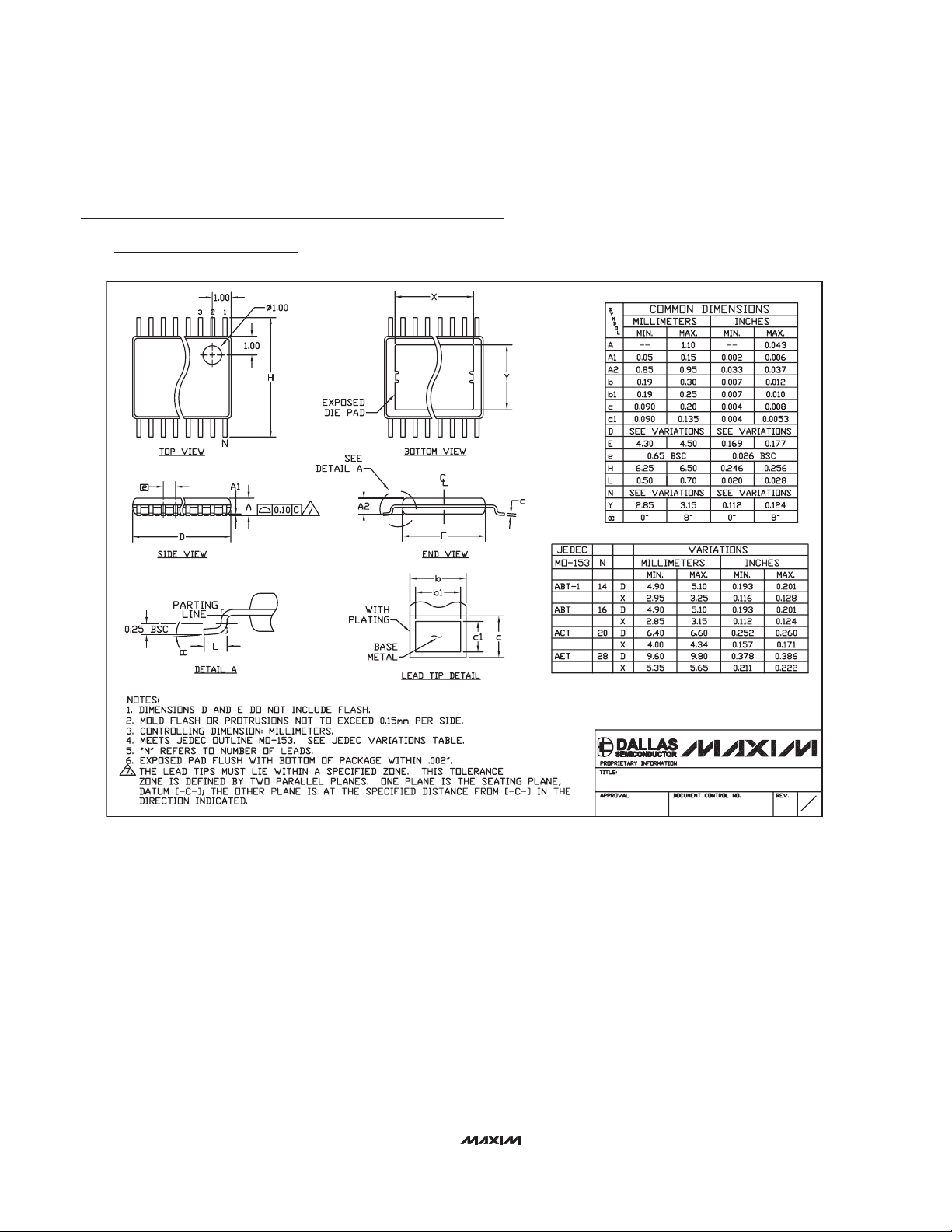
Package Information (continued)
(The package drawing(s) in this data sheet may not reflect the most current specifications. For the latest package outline information,
go to www.maxim-ic.com/packages
.)
TSSOP 4.4mm BODY.EPS
PACKAGE OUTLINE, TSSOP, 4.40 MM BODY
EXPOSED PAD
21-0108
1
D
1
 Loading...