

_______________General Description
The MAX3761/MAX3762 limiting amplifiers, with 4mV
sensitivity and PECL data outputs, are optimized for
operation in low-cost, 622Mbps, LAN/ATM LAN fiber
optics applications.
An integrated power detector senses the input signal’s
amplitude. A received-signal-strength indicator (RSSI)
gives an analog indication of the power level, while the
complementary loss-of-signal (LOS) outputs indicate if
the input power level exceeds the programmed
threshold level. The LOS threshold can be adjusted to
detect signal amplitudes between 3mVp-p and
100mVp-p, providing a 15dB LOS adjustment in fiber
optic receivers. The LOS outputs have 3.5dB of
hysteresis, which prevents chatter when input signal
levels are small. The MAX3761’s LOS outputs are compatible with TTL-logic levels. The MAX3762 has PECL
LOS outputs.
DISABLE and LOS can be used to implement a squelch
function, which turns off the data outputs when the
input signal is below the programmed threshold.
________________________Applications
622Mbps LAN/ATM LAN Receivers
155Mbps LAN/ATM LAN Receivers
____________________________Features
♦ Chatter-Free Power Detector with Programmable
Loss-of-Signal Outputs
♦ 4mV Input Sensitivity (PECL Loss-of-Signal
Interface Logic—MAX3766
♦ PECL Data Outputs
♦ Single 5V Power Supply
♦ 250ps Output Edge Speed
♦ Low 15ps Pulse-Width Distortion
♦ TTL Loss-of-Signal Interface Logic—MAX3761
MAX3761/MAX3762
Low-Power, 622Mbps Limiting Amplifiers
with Chatter-Free Power Detect for LANs
________________________________________________________________
Maxim Integrated Products
1
CZN
OUT+
OUT-
LOS-
LOS+
DISABLE
SUB
GND
GNDO
100pF
50Ω
CZP
R1
100k
R2
22k
+V
CC
VTH
INV
MAX3761
CAZ
150pF
50Ω
V
CC
- 2V
V
CC
EN
RSSI
VCCO
VIN+
10nF
100pF
BYPASS
SUPPLY
C
IN
5.6nF
C
IN
5.6nF
+5V
VINFILTER
C
FILTER
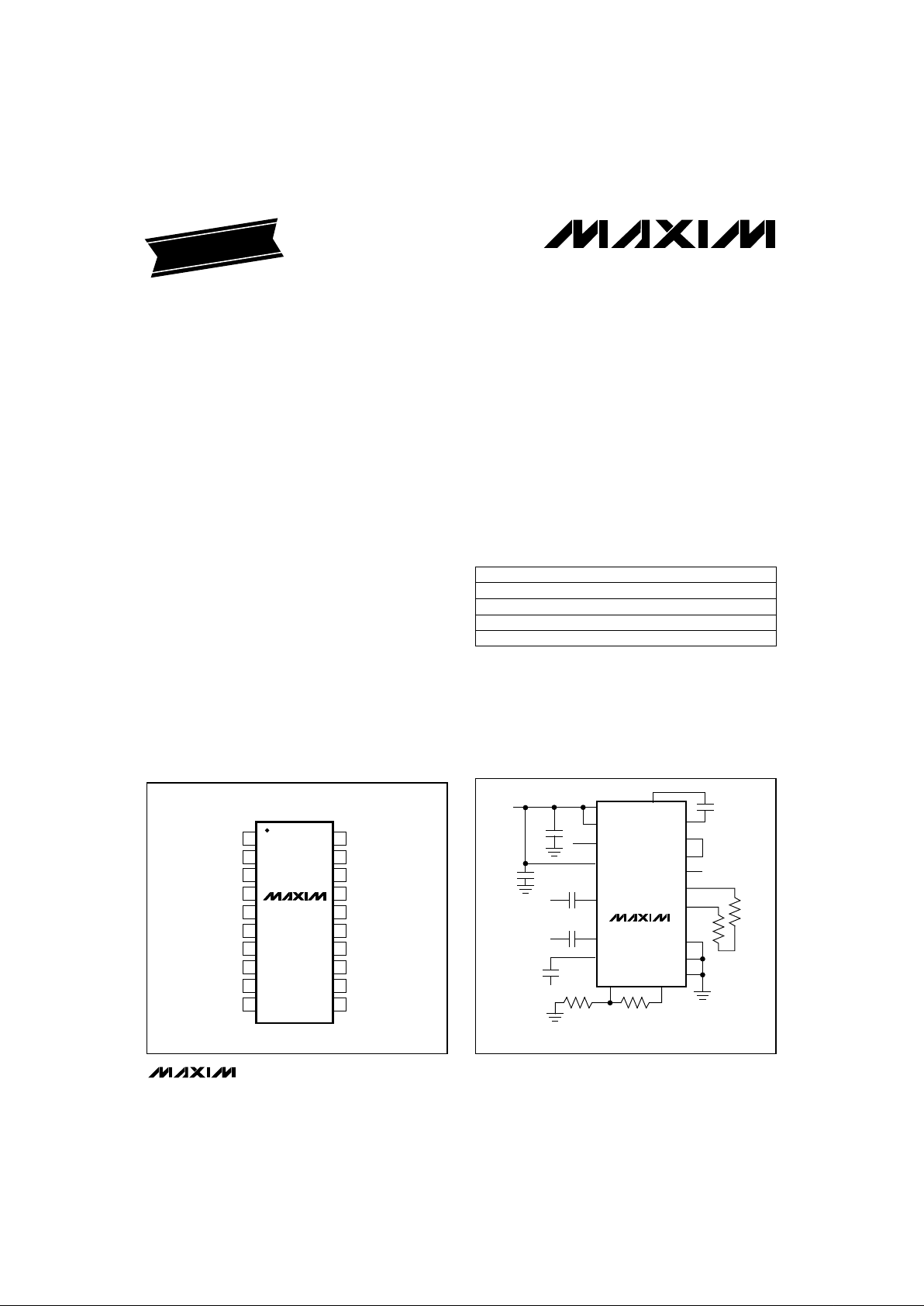
_________Typical Operating Circuits
19-1097; Rev 1; 9/96
PART
MAX3761EEP
MAX3761C/D
MAX3762EEP
-40°C to +85°C
-40°C to +85°C
-40°C to +85°C
TEMP. RANGE PIN-PACKAGE
20 QSOP
Dice*
20 QSOP
EVALUATION KIT
AVAILABLE
______________Ordering Information
*
Dice are designed to operate from -40°C to +85°C, but are
tested and guaranteed only at TA= +25°C.
For free samples & the latest literature: http://www.maxim-ic.com, or phone 1-800-998-8800
MAX3762C/D -40°C to +85°C Dice*
__________________Pin Configuration
20
19
18
17
16
15
14
13
1
2
3
4
5
6
7
8
DISABLE
LOS+
LOSV
CC
V
CC
EN
RSSI
FILTER
TOP VIEW
VCCO
OUT+
OUTGNDO
SUB
GND
VIN-
VIN+
12
11
9
10
VTH
INV
CZN
CZP
QSOP
MAX3761
MAX3762
MAX3762 at end of data sheet.
MAX3761/MAX3762
Low-Power, 622Mbps Limiting Amplifiers
with Chatter-Free Power Detect for LANs
2 _______________________________________________________________________________________
ABSOLUTE MAXIMUM RATINGS
DC ELECTRICAL CHARACTERISTICS
(VCC= +4.5V to +5.5V, DISABLE = low, TA= -40°C to +85°C, unless otherwise noted. Typical values are at VCC= +5.0V, TA= +25°C.)
(Note 1)
Stresses beyond those listed under “Absolute Maximum Ratings” may cause permanent damage to the device. These are stress ratings only, and functional
operation of the device at these or any other conditions beyond those indicated in the operational sections of the specifications is not implied. Exposure to
absolute maximum rating conditions for extended periods may affect device reliability.
Note 1: Dice are tested at TA = +25°C.
Note 2: Outputs terminated with 50Ω to V
CC
- 2V.
Note 3: Voltage measurements are relative to V
CC
.
V
CC
, VCCO............................................................-0.5V to +7.0V
FILTER, RSSI, EN, VIN+, VIN-, CZP, CZN,
DISABLE, LOS+, LOS-, INV, VTH...............-0.5V to (V
CC
+ 0.5V)
PECL Output Current (OUT+, OUT-, LOS+, LOS-) ............50mA
Continuous Power Dissipation (T
A
= +85°C)
QSOP (derate 8.3mW/°C above +70°C).......................667mW
Operating Junction Temperature Range...........-40°C to +150°C
Processing Temperature (die).........................................+400°C
Storage Temperature Range.............................-65°C to +160°C
Lead Temperature (soldering, 10sec).............................+300°C
MAX3762, I
VCC
MAX3761, I
VCC
DISABLE = high
DISABLE = high
MAX3761
MAX3761
(Notes 2, 3)
(Notes 2, 3)
Logic high
MAX3762 (Notes 2, 3)
MAX3761
MAX3761
MAX3762 (Note 3)
MAX3762 (Notes 2, 3)
MAX3762 (Note 3)
CONDITIONS
VVCC- 0.7 VCC-1.2Disabled Common-Mode Output
mV-100 100Disabled Differential Output
mV-1830 -1555PECL Data Output Voltage Low (VOL)
mV-1150 -880PECL Data Output Voltage High (VOH)
mV-1470DISABLE Input PECL Low
mV-1160DISABLE Input PECL High
mA
30 46
25 37
Power-Supply Current
V0.8DISABLE Input Low
V2.65DISABLE Input High
µA100DISABLE Input Current
mV-1830 -1555LOS Output PECL Low
V2.8LOS Output TTL High
V
0.40
LOS Output TTL Low
mV-1150 -880LOS Output PECL High
UNITSMIN TYP MAXPARAMETER
(TA= +25°C to +85°C)
(TA= -40°C to +25°C) 0.44
MAX3761/MAX3762
Low-Power, 622Mbps Limiting Amplifiers
with Chatter-Free Power Detect for LANs
_______________________________________________________________________________________ 3
AC ELECTRICAL CHARACTERISTICS
(VCC= +4.5V to +5.5V, PECL outputs terminated with 50Ω to VCC- 2V, input 4mV to 2Vp-p, TA= -40°C to +85°C, unless otherwise
noted. Typical values are at V
CC
= +5.0V, TA = +25°C.) (Note 5)
Note 5: AC parameters are guaranteed by design and characterization.
Note 6: Input signal is a 1-0 pattern, 622Mbps.
Note 7: PWD = [(width of wider pulse) - (width of narrower pulse)] / 2.
TA= -40°C, 2
23
- 1 PRBS
(Notes 6, 7)
(Note 6)
Differential
20% to 80%
CONDITIONS
Ω3900Input Resistance
psPulse-Width Distortion
mV3.2Minimum LOS Assert Input
15 80
%20Data-Output Overshoot
ps250Data-Output Edge Speed
UNITSMIN TYP MAXPARAMETER
__________________________________________Typical Operating Characteristics
(MAX3761/MAX3762 EV kit, VCC= +5.0V, PECL outputs terminated with 50Ωto VCC- 2V, input is a 1-0 pattern, 622Mbps, TA= +25°C,
unless otherwise noted.)
10
15
20
25
30
35
40
45
50
-40 -15 10 35 60 85
MAX3762
SUPPLY CURRENT vs. TEMPERATURE
MAX3761/62-01
AMBIENT TEMPERATURE (°C)
CURRENT (mA)
VCC = 5.5V
VCC = 5.0V
VCC = 4.5V
10 100 10001
INPUT SIGNAL (mVp-p)
RSSI VOLTAGE (V)
2.40
2.16
1.68
1.44
1.20
1.92
2.28
1.80
1.56
1.32
2.04
RSSI vs. INPUT AMPLITUDE
AND DATA PATTERN
MAX3761/62-02
2
23
- 1
PRBS PATTERN
1-0 PATTERN
2.40
1.20
-50 -40 -20 0
RSSI vs.
INPUT POWER AND FREQUENCY
1.44
2.16
MAX3761/62-03
INPUT POWER (dBm)
RSSI VOLTAGE (V)
-30 -10-45 -25 -5-35 -15
1.92
1.68
1.32
1.56
2.28
2.04
1.80
10MHz
500MHz
2
23
- 1 PRBS, VTH = 1.8V dB3.5LOS Hysteresis
100mV/
div
5µs/div
LOS OPERATION
WITH SQUELCHING
MAX3761/62-10
DATA IN
LOS+
OUT+
MAX3761/MAX3762
Low-Power, 622Mbps Limiting Amplifiers
with Chatter-Free Power Detect for LANs
4 _______________________________________________________________________________________
2.00
1.20
-40 -20 800 204060
RSSI vs. TEMPERATURE
(622Mbps 2
23
- 1 PRBS)
1.36
1.84
MAX3761/62-04
AMBIENT TEMPERATURE (°C)
RSSI VOLTAGE (V)
1.68
1.52
1.28
1.44
1.92
1.76
1.60
VIN = 50mVp-p
VIN = 16mVp-p
VIN = 4mVp-p
2.50
2.75
3.00
3.25
3.50
3.75
4.00
-40
-20
0 20406080100
LOS HYSTERESIS vs. TEMPERATURE
(622Mbps 2
23
- 1 PRBS PATTERN)
MAX3761/62-05
AMBIENT TEMPERATURE (°C)
HYSTERESIS (dB)
ASSERT LEVEL SET
TO APPROXIMATELY
2mVp-p
ASSERT LEVEL SET
TO APPROXIMATELY 30mVp-p
3
4
5
6
7
8
-40 0-20 20 40 60
80
100
LOS HYSTERESIS vs. TEMPERATURE
(622Mbps 1-0 PATTERN)
MAX3761/62-06
AMBIENT TEMPERATURE (°C)
HYSTERESIS (dB)
ASSERT LEVEL SET
TO APPROXIMATELY
2mVp-p
ASSERT LEVEL SET
TO APPROXIMATELY
30mVp-p
-0.8
-1.8
-40 -20
0
20 40 60 80
DATA OUTPUT LEVELS
(REFERENCE TO V
CC
)
-1.6
-1.0
MAX3761/62-07
AMBIENT TEMPERATURE (°C)
VOLTAGE (V)
-1.2
-1.4
VOH
VOL
1m 1010.10.01
INPUT SIGNAL (Vp-p)
DIFFERENTIAL OUTPUT (mV)
1400
1280
1160
0.1m
1040
800
680
560
440
200
320
920
DIFFERENTIAL OUTPUT
vs. INPUT AMPLITUDE
MAX3761/62-08
0.01 0.1 1 100.001
INPUT SIGNAL (Vp-p)
PULSE-WIDTH DISTORTION (PS)
50
40
20
10
0
30
PULSE-WIDTH DISTORTION
(622Mbps DATA RATE)
MAX3761/62-09
-40°C
+85°C
100mV/
div
5µs/div
DATA IN
LOS+
OUT+
LOS OPERATION
WITHOUT SQUELCHING
MAX3761/62-11
50mV/
div
500ps/div
DATA OUTPUT SINGLE-ENDED
(2
23
- 1 PRBS PATTERN)
MAX3761/62-12
INPUT = 4mVp-p
T
A
= +85°C
____________________________Typical Operating Characteristics (continued)
(MAX3761/MAX3762 EV kit, VCC= +5.0V, PECL outputs terminated with 50Ωto VCC- 2V, input is a 1-0 pattern, 622Mbps, TA= +25°C,
unless otherwise noted.)

MAX3761/MAX3762
Low-Power, 622Mbps Limiting Amplifiers
with Chatter-Free Power Detect for LANs
_______________________________________________________________________________________ 5
____________________________Typical Operating Characteristics (continued)
(MAX3761/MAX3762 EV kit, VCC= +5.0V, PECL outputs terminated with 50Ωto VCC- 2V, input is a 1-0 pattern, 622Mbps, TA= +25°C,
unless otherwise noted.)
______________________________________________________________Pin Description
NAME FUNCTION
1 FILTER Sets the integration frequency of the power detector. Impedance at this node is approximately 500Ω.
2 RSSI Received-Signal-Strength Indicator. An analog DC voltage representing the input power.
PIN
50mV/
div
500ps/div
DATA OUTPUT SINGLE-ENDED
(2
23
-1 PRBS PATTERN)
MAX3761/62-13
INPUT = 2Vp-p
T
A
= +85°C
200mV/
div
200ps/div
RANDOM JITTER
MAX3761/62-14
DIFFERENTIAL OUTPUT
(OUT+ - OUT-)
INPUT = 16mVp-p
T
A
= +27°C
1-0 PATTERN 622Mbps
10
4
10
5
10
6
10
3
FREQUENCY ON POWER SUPPLY (Hz)
RANDOM JITTER (ps rms)
10
8
4
2
6
RANDOM JITTER vs.
POWER-SUPPLY NOISE FREQUENCY
MAX3761/62-15
DIFFERENTIAL OUTPUT RANDOM JITTER
DATA INPUT AMPLITUDE = 16mVp-p
INPUT AMPLITUDE
POWER SUPPLY = 100mVp-p
3 EN Connect to VCC.
4, 17 V
CC
+5V Power Supply
5 VIN+ Positive Input Data
6 VIN- Negative Input Data
7 GND Supply Ground
8 SUB Substrate. Connect to ground.
9 CZP Sets input offset correction, low-frequency cutoff.
10 CZN Sets input offset correction, low-frequency cutoff.
11 INV Negative Input to Op Amp. Used for programming the loss-of-signal threshold.
12 VTH Loss-of-Signal Threshold Voltage
13 GNDO Ground Power Supply for Output Buffers
14 OUT- Negative PECL Data Output
15 OUT+ Positive PECL Data Output
16 VCCO +5V Power Supply for Output Buffers
18 LOS- Negative Loss-of-Power Flag, TTL (MAX3761) or PECL (MAX3762)
19 LOS+ Positive Loss-of-Power Flag, TTL (MAX3761) or PECL (MAX3762)
20 DISABLE Disables the data outputs when high. TTL (MAX3761) or PECL (MAX3762).

MAX3761/MAX3762
Low-Power, 622Mbps Limiting Amplifiers
with Chatter-Free Power Detect for LANs
6 _______________________________________________________________________________________
_______________Detailed Description
Figure 1 shows the functional diagram for the MAX3761/
MAX3762. The input signal is applied to VIN+ and VIN-.
A chain of amplifier stages, each contributing approximately 12.5dB of gain, amplifies the input signal to
PECL output voltage swings. A 4mVp-p input signal will
cause the output to fully limit.
Received-Signal-Strength
Indicator (RSSI)
Each amplifier stage contains a full-wave logarithmic
detector (FWD). The full-wave detector outputs are
summed at the FILTER pin and used to generate the
received-signal-strength indication (RSSI). The RSSI
output voltage is linearly proportional to the input power
(in decibels), and is approximated by:
where VINis the peak-to-peak input signal in millivolts.
The RSSI output is insensitive to fluctuations in temperature
and supply voltage. The power detector functions as a
broadband power meter that detects the total power of all
signals present in the passband of approximately 750MHz.
Refer to the
Typical Operating Characteristics
graphs show-
ing RSSI output versus input power and signal amplitude.
The high-speed RSSI signal is filtered with one external
capacitor connected from FILTER to VCC. The impedance at the FILTER pin is approximately 500Ω.
The FILTER capacitor (C
FILTER
) must be connected
to VCCfor proper operation.
Input-Offset Correction
The limiting amplifier provides approximately 60dB of
gain. An input DC offset of even 1mV reduces the
power-detection circuit’s accuracy and can cause the
output to limit. A low-frequency feedback loop is integrated into the MAX3761/MAX3762 to remove input offset. DC coupling the inputs is not recommended, as
this prevents the DC-offset-correction circuitry from
functioning properly. Input offset is typically reduced to
less than 100µV.
The capacitance between pins CZP and CZN, in parallel
with a 10pF integrated capacitance, determines the offset-correction circuit’s time constant. The input impedance between CZP and CZN is approximately 800kΩ.
The offset correction circuitry requires an average datainput duty cycle of 50%. If the input data has a different
average duty cycle, the output will have increased
pulse-width distortion.
V (V) = 1.13 + 0.457log (V )
RSSI IN
LIMITER
FWD
LIMITER
FWD
LIMITER
FWD
FILTER
REF
INV VTH
R1 R2
GNDO
LOS+/LOS-
V
CC
- 2V
RSSI
50Ω
OUT+/OUT-
DISABLE
VCCO ENCZN
C
AZ
CZPSUBGND
V
CC
VIN+/VIN-
C
IN
C
FILTER
V
CC
FWD = FULL-WAVE DETECTOR
LIMITER
FWD
MAX3761/MAX3762
Figure 1. Functional Diagram

Loss-of-Signal Indicator
The MAX3761/MAX3762 includes a loss-of-signal monitor with a programmable assert threshold and a hysteresis comparator. Internally, one comparator input is
tied to the RSSI output signal and the other is tied to the
threshold-voltage (VTH) pin, which provides a threshold
for the LOS indication. An op amp referenced to an
internal bandgap voltage (1.18V) is supplied for programming a supply-independent threshold voltage.
Only two external resistors are needed to program the
LOS assert level. VTH is programmable from 1.18V to
2.4V, providing adequate coverage of the RSSI output’s
useful range. The op amp runs on very low supply current and provides an accurate, temperature-stable
threshold, but can source only 20µA of current. For
proper operation, resistor R1 (see the
Typical
Operating Circuit
) should have a value ≥ 100kΩ. The
input bias current at INV is < 50nA.
To ensure chatter-free LOS operation, the internal LOS
comparator contains approximately 90mV of hysteresis.
The RSSI signal output has a slope of 25mV/dB.
Therefore, the overall circuit hysteresis is approximately
3.6dB[90mV / (25mV/dB)]. The LOS assert threshold is
45mV below VTH, while the LOS deassert threshold is
45mV above VTH.
Output Buffers
The DISABLE pin can be used to disable the dataoutput buffer. When DISABLE is high, the differential
output signal at OUT+ and OUT- is approximately zero.
In the disabled state, the common-mode voltage of
each output is approximately VCC- 0.8V. Connecting
DISABLE to LOS+ implements a squelch function. When
using the squelch function, the output signal is disabled
whenever the input signal is too small to be reliably
detected (as determined by the voltage at VTH). Use of
the disable function is recommended at all times.
The data outputs (OUT+ and OUT-) are implemented
with emitter followers that have output impedance of
approximately 2Ω. The MAX3762’s PECL LOS outputs
also are implemented with emitter followers that have
output impedance of approximately 2Ω.
The MAX3761 TTL LOS output buffers are open-collector transistors with 6kΩ internal pull-up resistors.
__________________Design Procedure
Supply Voltage
The MAX3761/MAX3762 can be operated with a single
+5V or -5V power supply.
Programming the LOS Assert Level
First determine the receiver system’s sensitivity in dBm
either by estimating or from prototyping results.
Estimate the total gain of the preamplifier and photodiode, then use Figure 3 to select resistor R2, placing the
LOS assert 3dB to 4dB below the receiver sensitivity.
Alternatively, use the
Typical Operating Characteristics
to select the VTHvalue needed for LOS assert, then
program VTHwith the following relation:
VTH= 1.18(1 + R2 / R1)
Select R1 ≥ 100kΩ.
MAX3761/MAX3762
Low-Power, 622Mbps Limiting Amplifiers
with Chatter-Free Power Detect for LANs
_______________________________________________________________________________________ 7
V
ASSERT
(min)
V
ASSERT
V
DEASSERT
(max)
V
DEASSERT
V
TH
1.2V
45mV
25mV/dB
45mV
INPUT SIGNAL AMPLITUDE
RSSI
VOLTAGE
3.6dB
typical
Figure 2. Loss-of-Signal Definitions
0
-38 -36 -28 -22
10
60
70
MAX3761/2-03
INPUT SIGNAL (dBm)
VALUE OF R2 (kΩ)
-32-34 -26-30 -24
40
20
80
50
30
GAIN = 2000
GAIN = 6000
R1 = 100kΩ
GAIN = 4000
Figure 3. Using TIA Gain and Photodiode Responsivity to
Select LOS Programming Resistor
GAIN IS PHOTODIODE RESPONSIVITY x TRANSIMPEDANCE GAIN.
EXTINCTION RATIO OF 10 IS ASSUMED.

MAX3761/MAX3762
Capacitor Selection
A typical MAX3761/MAX3762 implementation requires
four external capacitors. To select the capacitors, first
determine the following parameters in the receiver system (see the
Applications Information
section for recommendations in 622Mbps ATM and Fibre Channel
1063Mbps systems):
1) The duration of the expected longest run of consec-
utive bits in the data stream. For example, 72 consecutive zeros in a 622Mbps data stream have a
duration of 116ns.
2) The maximum allowable data-dependent jitter.
3) The desired power-detector integration time con-
stant [1/ (2πf
INT
)].
4) The transimpedance amplifier’s maximum peak-to-
peak output voltage.
Step 1. Select the Input AC-Coupling Capacitors (C
IN
).
When using a limiting preamplifier with a highpass
frequency response, select CINto provide a lowfrequency cutoff (fC) one decade lower than the
preamplifier low-frequency cutoff. This causes nearly all
data-dependent jitter (DDJ) to be generated in the preamplifer circuit. For example, if the preamplifier’s lowfrequency cutoff is 150kHz, then select CINto provide a
15kHz low-frequency cutoff.
Select CINwith the following equation:
For differential input signals, use a capacitor equal to
CINon both inputs (VIN+ and VIN-). For single-ended
input signals, one capacitor should be tied to VIN+ and
another should decouple VIN- to ground.
When using a preamplifier without a highpass
response, select CINto ensure that data-dependent jitter is acceptable. The following equation provides an
estimate for CIN:
where: tL= duration of the longest run of consecutive
bits with the same value (seconds); DDJ = maximum
allowable data-dependent jitter, peak-to-peak (seconds);
BW = typical system bandwidth, normally 0.6 to 1.0
times the data rate (hertz).
Regardless of which method is used to select CIN, the
maximum LOS assert time can be estimated from the
value of C
IN
. The following equation estimates LOS time
delay when the maximum-amplitude signal is instantaneously removed from the input, and when the FILTER
time constant is much faster than the input time constant (C
FILTER
< 0.4CIN):
t
LOS ASSERT
= 1950CINln(V
MAXp-p
/ V
ASSERTp-p
)
where V
MAXp-p
is the maximum output of the preampli-
fier, and V
ASSERTp-p
is the input amplitude that causes
LOS to assert. The equation describes the input capacitors’ discharge time, from maximum input to the LOS
threshold into the 1950Ω, single-ended input resistance.
Step 2. Select the Offset-Correction Capacitor (C
AZ
).
To maintain stability, it is important to keep a onedecade separation between fCand the low-frequency
cutoff associated with the DC-offset-correction circuit
(fOC).
The input impedance between CZP and CZN is
approximately 800kΩ in parallel with 10pF. As a result,
the low-frequency cutoff (fOC) associated with the DCoffset-correction loop is computed as follows:
where CAZis an optional external capacitor between
CZP and CZN.
If CINis known, then:
Step 3. Select the Power-Detect Integration Capacitor
(C
FILTER
). For 622Mbps ATM applications, Maxim rec-
ommends a filter frequency of 3MHz, which requires
C
FILTER
= 100pF. The integration frequency can be
selected lower to remove low-frequency noise, or to
prevent unusual data sequences from asserting LOS.
C
FILTER
= 1 / ( 2π500f
INT
)
where f
INT
is the integration frequency.
C
C
pF
AZ
IN
≥−
41
10
f =
1
2 800k
OC
πΩCpF
AZ
+
()
10
C
-
IN
L
≥
−
()()
t
DDJ BW
1950 105ln
.
C =
1
2 f 1950
IN
C
πΩ
Low-Power, 622Mbps Limiting Amplifiers
with Chatter-Free Power Detect for LANs
8 _______________________________________________________________________________________

__________Applications Information
Converting Average Optical Power to
Signal Amplitude
Many of the MAX3761/MAX3762’s specifications relate
to input-signal amplitude. When working with fiber optic
receivers, the input is usually expressed in terms of
average optical power and extinction ratio. The relations given in Table 1 are helpful for converting optical
power to input signal when designing with the
MAX3761/MAX3762.
In an optical receiver, the input voltage to the limiting
amplifier can be found by multiplying the relationship in
Table 1 with the photodiode responsivity (p) and transimpedance amplifier gain (G).
Optical Hysteresis
Power and hysteresis are often expressed in decibels.
By definition, decibels are always 10log (power). At the
inputs to the MAX3761/MAX3762 limiting amplifier, the
power is V
IN
2
/R. If a receiver’s optical input power (x)
increases by a factor of two, and the preamplifier is linear, then the voltage input to the MAX3761/MAX3762
also increases by a factor of two.
The optical power change is 10log(2x / x) = 10log(2) =
+3dB
At the MAX3761/MAX3762, the voltage change is:
In an optical receiver the dB change at the MAX3761/
MAX3762 will always equal 2x the optical dB change.
The MAX3761/MAX3762’s typical voltage hysteresis is
3.6dB. This provides an optical hysteresis of 1.8dB.
Input Sensitivity
The receiver’s gain sensitivity defines the smallest signal
input that results in fully limited PECL-compatible data
outputs. Smaller signals result in nonlimited outputs. The
MAX3761/MAX3762’s input sensitivity (S
GAIN
) is 4mVp-p:
SGAIN = 4mV
Optical gain sensitivity (in dBm) is:
In a receiver with G = 6kΩ, re= 10, and ρ = 0.8A/W,
gain sensitivity is 510nW, or -32.9dBm.
622Mbps ATM Component Selection
As an example, a preamplifier with a 150kHz lowfrequency cutoff and a 950mVp-p maximum output has
the best performance with the following selections:
CIN= 5.6nF, so that fC= 15kHz (one decade below the
150kHz cutoff)
CAZ= 150pF, so that fOC< 1.5kHz (one decade
below fC)
C
FILTER
= 100pF, so that the integration frequency
equals 3MHz.
These selections should provide data-dependent jitter
less than 110ps p-p when the input consists of PRBS
data with no more than 72 consecutive bits.
10log
S
2G
x x
GAIN
ρrr
e
e
+
−
1
1
1000
10 10 2 20 2 6
2
2
2
log
/
/
log( ) log( )
2y
()
===+
R
yR
dB
MAX3761/MAX3762
Low-Power, 622Mbps Limiting Amplifiers
with Chatter-Free Power Detect for LANs
_______________________________________________________________________________________ 9
Table 1. Optical-Power Relations*
TIME
P0
P1
P
AVE
Figure 4. Optical-Power Relations
SYMBOL RELATION
Average
Power
P
AVE
PARAMETER
Extinction
Ratio
r
e
Optical Power
of a “1”
P1
Optical Power
of a “0”
P0
Signal
Amplitude
P
IN
P = P0 + P1
AVE
()
/2
r = 1 / P0
e
P
PP
r
r
AVE
e
e
121=
+
PP r
AVE e
02 1=+
()
/
PPPP
r
r
IN AVE
e
e
=−=
−
()
+
102
1
1
OPTICAL
POWER
*
Assuming a 50% average input data duty cycle (true for SONET/ATM data).

MAX3761/MAX3762
For LOS assert at -35dBm, select R1 = 100kΩ and R2 =
22kΩ, which programs the LOS assert at input ≅ 3mV.
With this selection, LOS assert time will typically be less
than 85µs.
Fibre Channel Component Selection
In Fibre Channel applications, the desired LOS assert
time is typically 25µs maximum, and data-dependent
jitter is reduced by 8B10B coding techniques. The following are recommended in a Fibre Channel system
where preamp gain is 2000V/W, LOS assert is set for
-24dBm (13mV MAX3761/MAX3762 input), and the
maximum input to the MAX3761/MAX3762 is 1Vp-p:
CIN= 3.3nF (to provide LOS assert in 25µs)
CAZ= 82pF (to provide fOC= 1/10 fCfor stability)
C
FILTER
= 100pF (for a 3MHz integration constant)
R1 = 100kΩ, R2 = 50kΩ (to set LOS assert at -24dBm)
PECL Terminations
The standard PECL termination (50Ω to VCC- 2V) is
recommended for best performance and output characteristics. The data outputs operate at high speed,
and should always drive transmission lines with
50Ω to 75Ω terminations. Balanced termination is recommended for all outputs.
Figure 5 shows an alternative method for terminating
the data outputs. The technique provides approximately 8mA DC bias current, with a 50Ω AC load, for the
output termination. This technique is useful for viewing
the output on an oscilloscope or changing the PECL
reference voltage.
The MAX3762’s PECL LOS outputs are relatively slow
and do not need 50Ω terminations (although they are
capable of driving them). To reduce power, the
MAX3762’s LOS outputs can be terminated with 500Ω.
Figure 6 shows a typical operating circuit for the
MAX3762.
Wire Bonding
For high current density and reliable operation, the
MAX3761/MAX3762 use gold metalization. Make connections to the dice with gold wire only, and use ballbonding techniques (wedge bonding is not
recommended). Die-pad size is 4 mils square, with a
6 mil pitch. Die thickness is 12 mils (0.3mm).
Layout Techniques
The MAX3761/MAX3762 are high-frequency, highbandwidth circuits. To ensure stability, use good highfrequency layout techniques. Filter voltage supplies,
and keep ground connections short. Use multiple vias
where possible. Use controlled-impedance transmission lines to connect the MAX3761/MAX3762 data outputs to other circuits.
Low-Power, 622Mbps Limiting Amplifiers
with Chatter-Free Power Detect for LANs
10 ______________________________________________________________________________________
470Ω
DRIVING 50Ω TO GROUND
470Ω
50Ω
50Ω
OUT+
OUT-
MAX3761
Figure 5. Alternative PECL Termination

MAX3761/MAX3762
Low-Power, 622Mbps Limiting Amplifiers
with Chatter-Free Power Detect for LANs
______________________________________________________________________________________ 11
CZN
OUT+
OUT-
LOS-
LOS+
DISABLE
SUB
GND
GNDO
100pF
50Ω
500Ω
CZP
R1
R2
+V
CC
VTH
INV
MAX3762
CAZ
150pF
50Ω
V
CC
- 2V
V
CC
- 2V
VCC - 2V
V
CC
EN
RSSI
VCCO
VIN+
10nF
100pF
C
IN
5.6nF
C
IN
5.6nF
+5V
VIN-
FILTER
C
FILTER
500Ω
___________________Chip Topography
_____________________________________Typical Operating Circuits (continued)
0.063"
(1.60mm)
0.059"
(1.49mm)
CZP CZN INV VTH
LOS-
V
CC
VCCO
OUT+
OUTGNDO
RSSI
FILTER
DISABLE
LOS+
EN
V
CC
VIN+
VINGND
SUB
TRANSISTOR COUNT: 961
SUBSTRATE CONNECTED TO SUB

Maxim cannot assume responsibility for use of any circuitry other than circuitry entirely embodied in a Maxim product. No circuit patent licenses are
implied. Maxim reserves the right to change the circuitry and specifications without notice at any time.
12
__________________Maxim Integrated Products, 120 San Gabriel Drive, Sunnyvale, CA 94086 (408) 737-7600
© 1996 Maxim Integrated Products Printed USA is a registered trademark of Maxim Integrated Products.
MAX3761/MAX3762
Low-Power, 622Mbps Limiting Amplifiers
with Chatter-Free Power Detect for LANs
________________________________________________________Package Information
DIM
A
A1
A2
B
C
D
E
e
H
h
L
N
S
α
MIN
0.061
0.004
0.055
0.008
0.0075
0.150
0.230
0.010
0.016
0°
MAX
0.068
0.0098
0.061
0.012
0.0098
0.157
0.244
0.016
0.035
8°
MIN
1.55
0.127
1.40
0.20
0.19
3.81
5.84
0.25
0.41
0°
MAX
1.73
0.25
1.55
0.31
0.25
3.99
6.20
0.41
0.89
8°
INCHES MILLIMETERS
21-0055A
QSOP
QUARTER
SMALL-OUTLINE
PACKAGE
DIM
D
S
D
S
D
S
D
S
MIN
0.189
0.0020
0.337
0.0500
0.337
0.0250
0.386
0.0250
MAX
0.196
0.0070
0.344
0.0550
0.344
0.0300
0.393
0.0300
MIN
4.80
0.05
8.56
1.27
8.56
0.64
9.80
0.64
MAX
4.98
0.18
8.74
1.40
8.74
0.76
9.98
0.76
INCHES MILLIMETERS
PINS
16
16
20
20
24
24
28
28
L
α
H
A2
E
E
D
e
A
A1
C
B
S
N
h x 45°
SEE PIN COUNT VARIATIONS
SEE PIN COUNT VARIATIONS
SEE PIN COUNT VARIATIONS
0.635 BSC0.25 BSC
 Loading...