

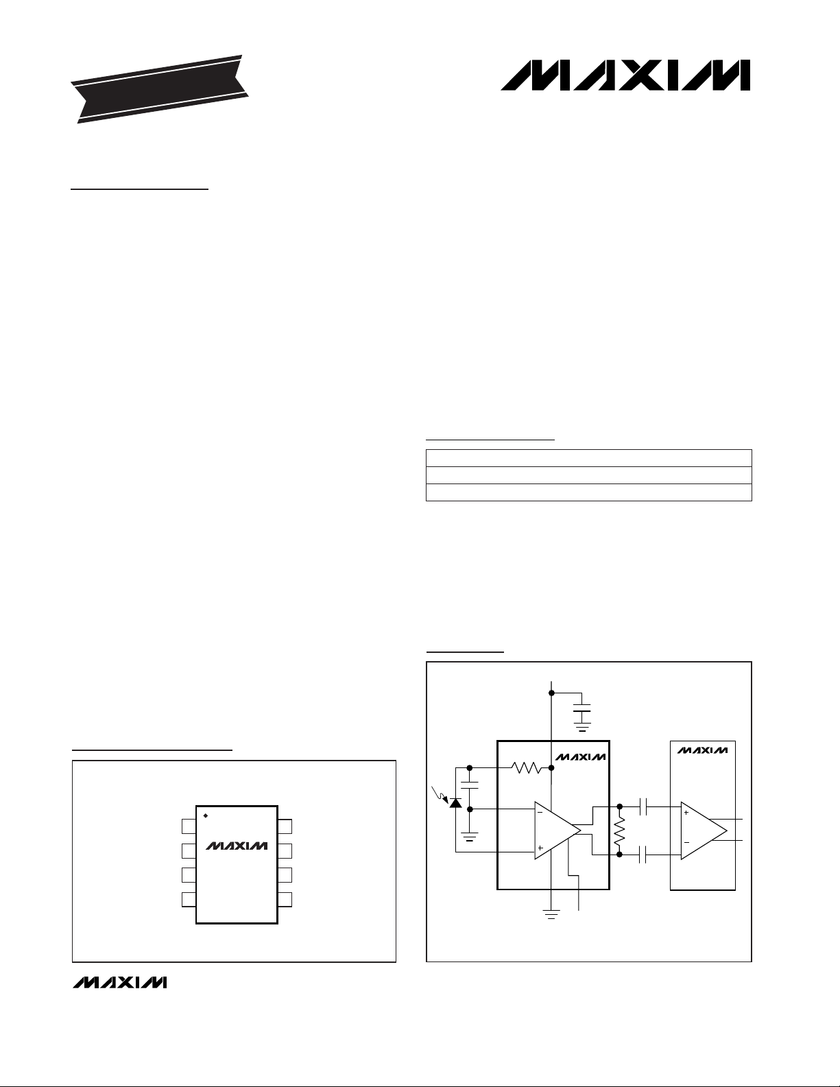
General Description
The MAX3760 is a transimpedance preamplifier for
622Mbps ATM applications. It operates from a single
+5V supply and typically consumes only 100mW
power. The preamplifier converts a small photodiode
current to a differential voltage. A DC cancellation circuit provides a true differential output swing over a
wide range of input current levels, thus reducing pulsewidth distortion.
6.5kΩ transimpedance gain and 560MHz bandwidth,
combined with low 73nA input-referred noise, provide
-31.5dBm typical sensitivity in 1300nm receivers. The
circuit accepts a 1mAp-p input current, resulting in a
typical optical overload of -3dBm. The device operates
over an extended temperature range of -40°C to +85°C.
The MAX3760 is internally compensated and requires
few external components. In die form it includes a
space-saving filter connection, which provides positive
bias for the photodiode through a 1kΩ resistor to VCC.
These features, combined with the die aspect ratio and
dimensioning, allow the MAX3760 to assemble easily
into a TO-style header with a photodiode.
The MAX3760 is designed to be used with either the
MAX3761 or the MAX3762 limiting-amplifier ICs. When
combined with a photodiode, the chipset forms a complete 5V, 622Mbps receiver. The MAX3760 is available
in die form and in an 8-pin SO package.
________________________Applications
622Mbps ATM LAN Optical Receivers
622Mbps WAN Optical Receivers
____________________________Features
♦ 73nA RMS Input-Referred Noise
♦ 560MHz Bandwidth
♦ 1mA Peak Input Current
♦ 6.5kΩ Gain
♦ Operation from -40°C to +85°C
♦ 100mW Typical Power Consumption
♦ Single +5V Supply
MAX3760
622Mbps, Low-Noise Transimpedance
Preamplifier for LAN and WAN Optical Receivers
________________________________________________________________
Maxim Integrated Products
1
MAX3760
MAX3761
MAX3762
LIMITING
AMPLIFIER
(FILTER)
OUT+
0.01µF
0.01µF
+5V
0.01µF
100Ω
(OPTIONAL)
OUT-
GND COMP*
100pF
( ) INDICATE PINS AVAILABLE ONLY ON THE DIE.
*NOT CONNECTED
1k
V
CC
INREF
IN
Typical Application Circuit
OUT-
INREF
GND
GND
1
2
8
7
COMP
OUT+
IN
V
CC
MAX3760
SO
TOP VIEW
3
4
6
5
Pin Configuration
19-4765; Rev 0; 7/98
PART
MAX3760ESA
MAX3760E/D -40°C to +85°C
-40°C to +85°C
TEMP. RANGE PIN-PACKAGE
8 SO
Dice*
EVALUATION KIT
AVAILABLE
Ordering Information
*
Dice are designed to operate over a -40°C to +100°C junction
temperature (T
j
) range, but are tested and guaranteed at
T
A
= +25°C.
For free samples & the latest literature: http://www.maxim-ic.com, or phone 1-800-998-8800
For small orders, phone 408-737-7600 ext. 3468.
MAX3760
622Mbps, Low-Noise Transimpedance
Preamplifier for LAN and WAN Optical Receivers
2 _______________________________________________________________________________________
ABSOLUTE MAXIMUM RATINGS
DC ELECTRICAL CHARACTERISTICS
(VCC= +4.5V to +5.5V, COMP = GND, 100Ω load between OUT+ and OUT-, TA= -40°C to +85°C, unless otherwise noted. Typical
values are at V
CC
= +5.0V, TA= +25°C.) (Note 1)
AC ELECTRICAL CHARACTERISTICS
(VCC= +4.5V to +5.5V, COMP = open, CIN= 0.75pF, outputs terminated differentially into 100Ω, 8-pin SO package in MAX3760
EV kit, T
A
= +25°C, unless otherwise noted. Typical values are at VCC= +5V.) (Notes 2, 3)
Stresses beyond those listed under “Absolute Maximum Ratings” may cause permanent damage to the device. These are stress ratings only, and functional
operation of the device at these or any other conditions beyond those indicated in the operational sections of the specifications is not implied. Exposure to
absolute maximum rating conditions for extended periods may affect device reliability.
Note 1: Dice are tested at TA= +25°C.
Note 2: AC characteristics are guaranteed by design and characterization.
Note 3: C
IN
is the source capacitance presented to the die. Includes package parasitic, photo diode, and parasitic interconnect
capacitance.
Note 4: Input is a 622Mbps 1-0 pattern, signal amplitude = 0 to 1mA, extinction ratio (r
e
) = 10.
Note 5: Measured with a 4-pole, 470MHz Bessel filter.
V
CC
........................................................................-0.5V to +7.0V
Continuous Current
IN, FILTER..........................................................-5mA to +5mA
OUT+, OUT-...................................................-25mA to +25mA
Voltage at INREF...................................................-0.5V to +0.5V
Voltage at COMP........................................-0.5V to (V
CC
+ 0.5V)
Continuous Power Dissipation (T
A
= +85°C)
SO (derate 5.88mW/°C above +85°C)..........................383mW
Storage Temperature Range.............................-65°C to +160°C
Lead Temperature (soldering, 10sec).............................+300°C
Operating Junction Temperature Range (die).....-55°C to +150°C
Processing Temperature (die).........................................+400°C
Differential output, input <10µA
Input = open
Input = open
IIN= 500µA, COMP = open
IIN= 500µA, total peak-to-peak,
differential signal
CONDITIONS
kΩ5.2 6.5 7.8z
21
Small-Signal Transimpedance
mA20 30I
CC
V0.8 0.95V
IN
Input Bias Voltage
Supply Current
Ω800 1000 1200R
FILTER
FILTER Resistance
VVCC- 2.0Output Common-Mode Level
mV-25 25V
OS
Differential Output Offset
Ω40 50 60Z
OUT
Output Impedance (per side)
mV550 950V
OUT(MAX)
Maximum Differential
Output Voltage
UNITSMIN TYP MAXSYMBOLPARAMETER
(Note 4)
20µA average input current
CIN= 0.75pF (Notes 3, 5)
CONDITIONS
ps75 200PWDPulse-Width Distortion
kHz50
MHz455 565BWSmall-Signal Bandwidth
Low-Frequency Cutoff
73 93.5 nAi
n
RMS Noise Referred to Input
UNITSMIN TYP MAXSYMBOLPARAMETER
f < 1MHz, referred to output dB20 45PSRRPower-Supply Rejection Ratio
200 psDDJData-Dependent Jitter
MAX3760
622Mbps, Low-Noise Transimpedance
Preamplifier for LAN and WAN Optical Receivers
_______________________________________________________________________________________
3
110
40
-40 30 100
INPUT-REFERRED NOISE
vs. JUNCTION TEMPERATURE
60
70
50
90
100
80
MAX3760-01
JUNCTION TEMPERATURE (°C)
INPUT-REFERRED NOISE (nA)
-5 65
470MHz BANDWIDTH
CIN = 1.25pF
CIN = 0.25pF
CIN = 0.75pF
CIN IS SOURCE CAPACITANCE
PRESENTED TO DIE. INCLUDES PACKAGE
PARASITIC, PIN DIODE, AND PARASITIC
INTERCONNECT CAPACITANCE
80
78
76
10k 100k 10M 10G
SMALL-SIGNAL GAIN
vs. FREQUENCY
62
60
72
70
74
68
MAX3760-02
FREQUENCY (Hz)
GAIN (dB)
1M 100M
64
66
1G
0
50
100
150
200
0 400200 600 800 1000
PULSE-WIDTH DISTORTION vs.
INPUT SIGNAL AMPLITUDE
MAX3760-03
INPUT SIGNAL AMPLITUDE (µAp-p)
PWD (ps)
re = 10
622Mbps,
ONE-ZERO PATTERN
0
100
50
250
200
150
350
400
300
450
1.00 10.0 21.52.15 4.64 46.4 100 215 464 1000
INPUT-REFERRED RMS NOISE CURRENT
vs. DC INPUT CURRENT
MAX3760toc04
DC INPUT CURRENT (µA)
INPUT-REFERRED NOISE (nA)
CIN = 0.75pF
470MHz BANDWIDTH
1.0
1.3
1.2
1.1
1.4
1.5
1.6
10 15010020 50 200 250 300 400 500 600
TYPICAL EYEWIDTH vs. INPUT SIGNAL
MAX3760 toc07
INPUT SIGNAL (µA)
EYEWIDTH (ns)
TA = -40°C
TA = +85°C
TA = +25°C
5000
5500
6000
6500
7000
-40 20-20 0 40 60 80 100
TRANSIMPEDANCE
vs. AMBIENT TEMPERATURE
MAX3760-05
AMBIENT TEMPERATURE (°C)
TRANSIMPEDANCE (Ω)
540
420
-40 30 100
TYPICAL BANDWIDTH
vs. JUNCTION TEMPERATURE
460
440
480
500
520
MAX760toc06
JUNCTION TEMPERATURE (°C)
3dB BANDWIDTH (MHz)
-5 65
CIN IS SOURCE CAPACITANCE
PRESENTED TO DIE. INCLUDES PACKAGE
PARASITIC, PIN DIODE, AND PARASITIC
INTERCONNECT CAPACITANCE
CIN = 0.25pF
CIN = 0.75pF
CIN = 1.25pF
IN TO-56 HEADER
0
200
400
600
800
0 400200 600 800 1000
DATA-DEPENDENT JITTER
vs. INPUT SIGNAL AMPLITUDE
MAX3760-08
INPUT SIGNAL AMPLITUDE (µAp-p)
JITTER (ps pp)
2
23
- 1 PRBS
622Mbps
r
e
= 10
-3.0
-2.4
-2.6
-2.8
-2.0
-2.2
-1.2
-1.4
-1.6
-1.8
-1.0
-40 20-20 0 40 60 80 100
OUTPUT COMMON-MODE VOLTAGE
vs. AMBIENT TEMPERATURE
MAX3760-09
AMBIENT TEMPERATURE (°C)
VOLTAGE (V)
REFERENCED TO V
CC
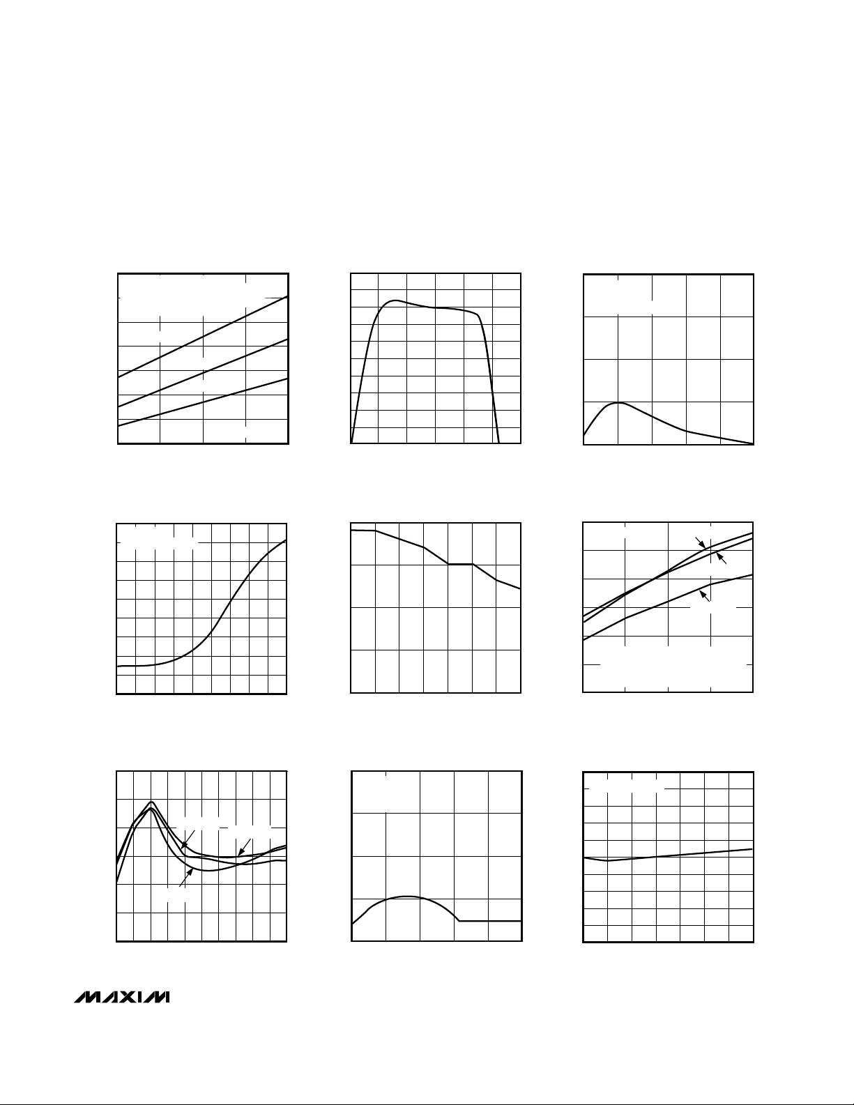
__________________________________________Typical Operating Characteristics
(MAX3760 EV kit, VCC= +5.0V, COMP = open, TA= +25°C, unless otherwise noted.)

400
500
600
700
800
-40 20-20 0 40 60 80 100
MAXIMUM OUTPUT SIGNAL AMPLITUDE
vs. AMBIENT TEMPERATURE
MAX3760-10
AMBIENT TEMPERATURE (°C)
MAX OUTPUT SIGNAL AMPLITUDE (mVp-p)
10mV/
div
50mV
-50mV
200ps/div
EYE DIAGRAM
(INPUT = 10µA)
MAX3760-11
2
23
- 1 PRBS
100mV/
div
500mV
-500mV
200ps/div
EYE DIAGRAM
(INPUT = 1mA)
MAX3760-12
2
23
- 1 PRBS
Pin Description
NAME FUNCTION
1 V
CC
Supply-Voltage Input
2 IN Signal Input
PIN
3 INREF Input Reference Connection. Connect to photodetector AC ground.
8 COMP
Compensation Capacitor Connection. Connection for optional external compensation capacitor for DCcancellation circuit. Add capacitance here to reduce the low-frequency cutoff of the DC cancellation circuit.
Connect COMP directly to GND to disable the DC cancellation circuit.
7 OUT+ Noninverting Voltage Output. Current flowing into the input causes OUT+ to increase.
6 OUT- Inverting Voltage Output. Current flowing into the input causes OUT- to decrease.
4, 5 GND Ground
— FILTER
Filter Connection. Provides positive bias for photodiode through a 1kΩ resistor to VCC(see the
Designing
Filters
section). Available on the die only.
MAX3760
622Mbps, Low-Noise Transimpedance
Preamplifier for LAN and WAN Optical Receivers
4 _______________________________________________________________________________________
Typical Operating Characteristics (continued)
(MAX3760 EV kit, VCC= +5.0V, COMP = open, TA= +25°C, unless otherwise noted.)

Detailed Description
The MAX3760 is a transimpedance amplifier designed
for 622Mbps fiber optic applications. As shown in the
Functional Diagram (Figure 1), it comprises a transimpedance amplifier, a paraphase amplifier with emitterfollower outputs, and a DC cancellation circuit.
Transimpedance Amplifier
The signal current at the input flows into a high-gain
amplifier’s summing node. Shunt feedback through RF
converts this current to a voltage with 6.5kΩ gain.
Diode D1 clamps the output voltage for large input currents. INREF is a direct connection to the input transistor’s emitter, and must be connected directly to the
photodetector AC ground return for best performance.
Paraphase Amplifier
The paraphase amplifier converts single-ended signals to
differential signals and introduces a voltage gain of 2.
This signal drives a pair of internally biased emitter followers, Q2 and Q3, which form the output stage. Resistors
R1 and R2 provide back-termination at the output, delivering a 100Ω differential output impedance. The output
emitter followers are designed to drive a 100Ω differential
load between OUT+ and OUT-. The MAX3760 can also
be terminated with higher output impedances for
increased gain and output voltage swing.
The MAX3760
will not drive a 50Ωload to ground.
For best noise rejec-
tion, terminate the MAX3760 with differential loads.
DC Cancellation Circuit
The DC cancellation circuit removes the input signal’s
DC component by employing low-frequency feedback.
This feature centers the input signal within the transimpedance amplifier’s dynamic range, thereby reducing
pulse-width distortion on large input signals.
The paraphase amplifier’s output is sensed through
resistors R3 and R4, then filtered, amplified, and fed
back to the base of transistor Q4. The transistor draws
the input signal’s DC component away from the transimpedance amplifier’s summing node.
The MAX3760 DC cancellation loop is internally compensated and does not require external capacitors in
most 622Mbps applications. Add external capacitance
at the COMP pin to reduce the DC cancellation circuit’s
frequency response and improve data-dependent jitter.
Connecting the COMP pin directly to GND disables the
circuit. The DC cancellation circuit can sink up to 1mA
at the input.
MAX3760
622Mbps, Low-Noise Transimpedance
Preamplifier for LAN and WAN Optical Receivers
_______________________________________________________________________________________ 5
MAX3760
IN
Q4
Q1
Q3
R2
R1
1k
Q2
RF
D1
R4
R3
V
CC
(FILTER)
OUT-
OUT+
GND
COMP
V
CC
V
CC
V
CC
DC
CANCELLATION
AMPLIFIER
TRANSIMPEDANCE
AMPLIFIER
PARAPHASE
AMP
GND
INREF
( ) INDICATE PINS AVAILABLE ON DIE ONLY.
Figure 1. Functional Diagram

MAX3760
The MAX3760 minimizes pulse-width distortion for data
sequences exhibiting a 50% duty cycle. A duty cycle
significantly different from 50% will cause the MAX3760
to generate pulse-width distortion.
DC cancellation current is drawn from the input and
creates noise. This is not a problem for low-level signals
with little or no DC component. Preamplifier noise
increases for signals with significant DC component
(see
Typical Operating Characteristics
).
The MAX3760 operates with the photodetector cathode
connected to VCC, as shown in the
Typical Application
Circuit
. Connecting the photodetector anode to GND
and the cathode to IN defeats the DC cancellation circuit and causes pulse-width distortion.
Input Reference
INREF is the reference point for IN. Connect it as close
as possible to the photodetector diode’s AC ground. The
photodetector’s AC ground is usually the ground of the
photodetector’s filter capacitor. The total length from
INREF, through the filter capacitor and the diode, and
back to the input should be no more than 2cm.
Applications Information
Optical Power Definitions
Many of the MAX3760’s specifications relate to the
input signal amplitude. When working with fiber optic
receivers, the optical input is usually expressed in
terms of average optical power and extinction ratio.
Use the relations given in Table 1 to convert optical
power to input signal when designing with the
MAX3760.
Calculating Sensitivity,
Overload, and Linear Range
Sensitivity Calculation
The MAX3760’s input-referred RMS noise current (in)
generally dominates the receiver sensitivity. In a system
where the bit error rate (BER) is 1E - 10, the signal-tonoise ratio must always exceed 12.7. The sensitivity,
expressed in average power, can be estimated as:
Where ρ is the photodiode responsivity in A/W.
Input Overload
The overload is the largest input that the MAX3760
accepts while meeting specifications. It is calculated
as:
Linear Range
The MAX3760 has high gain, which limits the output
when the input signal exceeds 20µAp-p. It operates
with 90% linearity for inputs not exceeding the following:
10log
20 A r 1
r - 1
1000 dBm
e
e
µ
ρ
+
( )
( )
Overload = 10log
1mA
2ρ
1000
dBm
Sensitivity = 10log
12.7i r + 1
2 r - 1
n e
e
( )
( )
ρ
1000 dBm
622Mbps, Low-Noise Transimpedance
Preamplifier for LAN and WAN Optical Receivers
6 _______________________________________________________________________________________
P1
OPTICAL
POWER
P
AVE
P0
TIME
Figure 2. Optical Power Definitions
SYMBOL RELATION
Average
Power
P
AVE
Extinction
Ratio
r
e
PARAMETER
Optical Power
of a “1”
P1
Optical Power
of a “0”
P0
Signal
Amplitude
P
IN
Table 1. Optical Power Relations
Note:
Assuming a 50% average input duty cycle.
P = P0 + P1
AVE
( )
/ 2
r = 1 / P0
e
P
P1 2P
r
(r 1)
AVE
e
e
=
+
P P r
AVE e
0 2 1 / = +
( )
P P1 - P0 2P
r - 1
(r 1)
IN AVE
e
e
= =
( )
+

Power Supply
The MAX3760 can operate from a power-supply voltage (VCC- GND) between 4.5V and 5.5V. GND can be
any stable voltage, including -5.0V, as found in many
systems using ECL interface levels.
Layout Considerations
Use good high-frequency design and layout techniques. The use of a multilayer circuit board with separate ground and VCCplanes is recommended. Take
care to bypass VCCand to connect the GND pin to the
ground plane with the shortest possible traces.
Designing a Low-Capacitance Input
Noise performance and bandwidth will be adversely
affected by stray capacitance at IN. Make every effort
to minimize capacitance on this node. Select a lowcapacitance photodiode and use good high-frequency
design and layout techniques. The MAX3760 is optimized for 0.75pF of capacitance on the input—approximately the capacitance of a low-cost photodetector
packaged in a header.
When using the MAX3760 in the SO package, note that
the package capacitance is about 0.3pF. The PC board
between the MAX3760 input and the photodetector will
add parasitic capacitance. Keep the input line short,
and remove power and ground planes beneath it.
For the best possible performance, assemble the
MAX3760 in die form using chip-and-wire technology,
or package the die in a TO header. These techniques
minimize parasitic capacitance, resulting in the lowest
noise.
Designing Filters
The MAX3760’s noise performance is strongly affected
by the circuit’s bandwidth, which changes over temperature and varies from lot to lot. Receiver sensitivity can
be improved by adding filters to limit this bandwidth.
Filter designs range from a one-pole filter using a single
capacitor to more complex filters using inductors. The
simple filter provides a moderate rolloff with minimal
components, while the complex filter provides a sharper rolloff and better transient response. A simple
530MHz filter can be created by placing a 6pF capacitor between the OUT+ and OUT- pins.
Supply-voltage noise at the photodiode cathode produces a current, I = C
PHOTO
∆V/∆t, which reduces
receiver sensitivity (C
PHOTO
is the photodiode capacitance.) The MAX3760’s FILTER resistor, combined with
an external capacitor, can be used to reduce this noise
(see
Typical Application Circuit
). Current generated by
supply-noise voltage is divided between C
FILTER
and
C
PHOTO
. The input noise current due to supply noise is
as follows (assuming the filter capacitor is much larger
than the photodiode capacitance):
If the amount of tolerable noise is known, the filter
capacitor is easy to select, as follows:
For example, with maximum noise voltage = 10mV
RMS
,
C
PHOTO
= 0.75pF, R
FILTER
= 1kΩ, and I
NOISE
selected
to be 30nA (half the MAX3760’s input noise):
C =
10mV
-
FILTER
( )( )
( )( )
=
0 75
1000 30 9
250
.
pF
E
pF
C >
V
FILTER
NOISE
( )( )
( )( )
C
R I
PHOTO
FILTER NOISE
I =
V
NOISE
NOISE
( )( )
( )( )
C
R C
PHOTO
FILTER FILTER
MAX3760
622Mbps, Low-Noise Transimpedance
Preamplifier for LAN and WAN Optical Receivers
_______________________________________________________________________________________ 7
C
FILTER
V
CC
OUT+OUT-
PHOTODIODE
CASE IS GROUND
TOP VIEW OF TO-56 HEADER
Figure 3. Suggested Layout for TO-56 Header

MAX3760
622Mbps, Low-Noise Transimpedance
Preamplifier for LAN and WAN Optical Receivers
8 _______________________________________________________________________________________
Wire Bonding
For high current density and reliable operation, the
MAX3760 uses gold metalization. Make connections to
the die with gold wire only, using ball-bonding techniques. Wedge bonding is not recommended. Die-pad
size is 4 mils square, with 6 mil pitch. Die thickness is
15 mils.
___________________Chip Topography
TRANSISTOR COUNT: 131
SUBSTRATE CONNECTED TO GND
0.042"
(1.05mm)
INREF FILTER IN
0.030"
(0.75mm)
GND
GND
OUT-
V
CC
COMP
OUT+
Package Information
SOICN.EPS
 Loading...