

For free samples & the latest literature: http://www.maxim-ic.com, or phone 1-800-998-8800.
For small orders, phone 1-800-835-8769.
General Description
The MAX3750/MAX3751 are +3.3V, Fibre Channel port
bypass ICs that include a high-speed multiplexer and
output buffer stage for hot swapping a storage device.
These devices are optimized for use in a Fibre Channel
arbitrated loop topology.
The MAX3750 has a 2.125Gbps data rate, while the
MAX3751’s data rate is 1.0625Gbps. Total power consumption (including output currents) is low: just 190mW
for the MAX3750 and 180mW for the MAX3751. Low
10ps jitter makes these devices ideal for cascaded
topologies. The output driver circuitry is tolerant of load
mismatches commonly caused by board vias and
inductive connectors. On-chip termination reduces
external part count and simplifies board layout.
Applications
2.125Gbps Fibre Channel Arbitrated Loop
1.0625Gbps Fibre Channel Arbitrated Loop
Mass Storage Systems
RAID/JBOD Applications
Features
♦ Single +3.3V Supply
♦ Low Jitter: 10ps
♦ Low Power Consumption
190mW (MAX3750)
180mW (MAX3751)
♦ Large Output Signal Swing: >1000mVp-p
♦ Mismatch Tolerant Output Driver Stage
♦ 150Ω Differential On-Chip Termination on All Inputs
♦ 150Ω On-Chip Back Termination on All Output
Ports
MAX3750/MAX3751
+3.3V, 2.125Gbps/1.0625Gbps
Fibre Channel Port Bypass ICs
________________________________________________________________
Maxim Integrated Products
1
19-4792; Rev 1; 1/99
PART
MAX3750CEE
MAX3751CEE
0°C to +70°C
0°C to +70°C
TEMP. RANGE PIN-PACKAGE
16 QSOP
16 QSOP
EVALUATION KIT
AVAILABLE
Pin Configuration appears at end of data sheet.
Ordering Information
LIN+
LIN-
LOUT+
LOUT-
FC-AL
DISK DRIVE
V
CC
RXTX
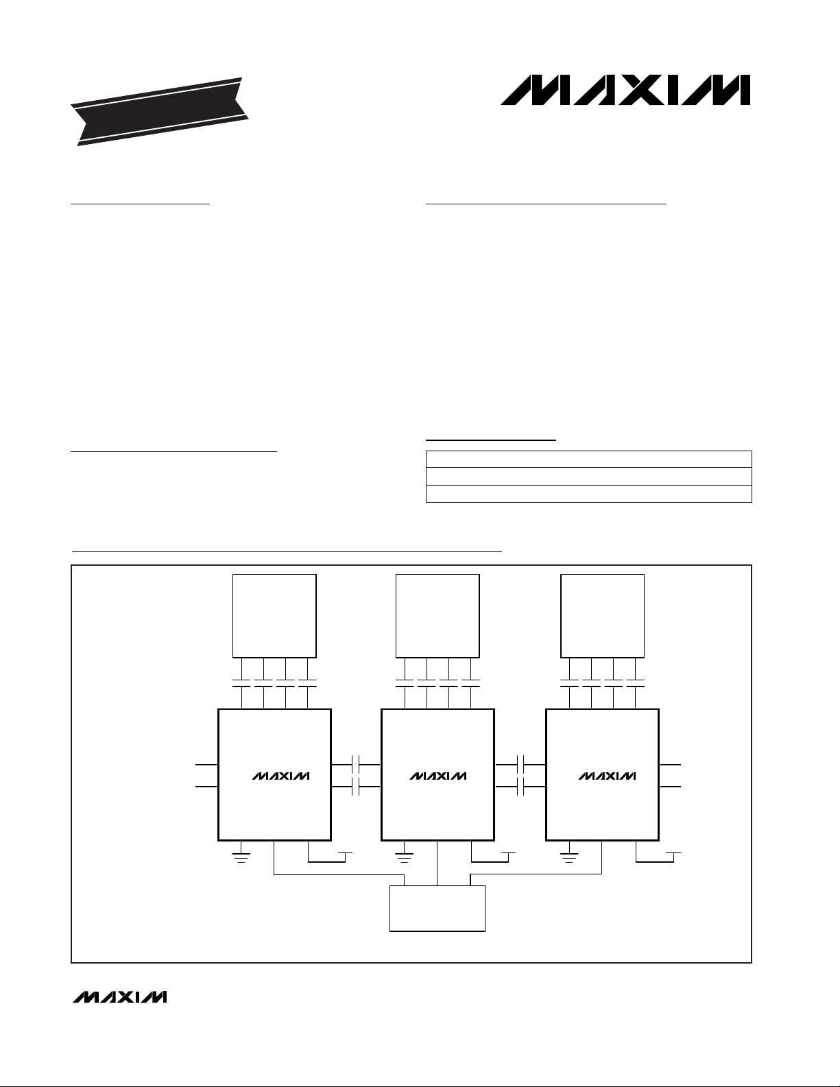
3.3V
SEL
C1–C8 = 100nF
THREE MAX3750/MAX3751s CASCADED IN AN FC-AL APPLICATION
GND
OUT+
OUT-
IN+
IN-
C7
C8
C2
C1
MAX3750
MAX3751
C3
C4
MICROPROCESSOR
LIN+
LIN-
LOUT+
LOUT-
FC-AL
DISK DRIVE
V
CC
RXTX
3.3V
SEL
GND
OUT+
OUT-
IN+
IN-
MAX3750
MAX3751
LIN+
LIN-
LOUT+
LOUT-
FC-AL
DISK DRIVE
V
CC
RXTX
3.3V
SEL
GND
OUT+
OUT-
IN+
IN-
MAX3750
MAX3751
C5
C6
Typical Application Circuit
MAX3750/MAX3751
+3.3V, 2.125Gbps/1.0625Gbps
Fibre Channel Port Bypass ICs
2 _______________________________________________________________________________________
ABSOLUTE MAXIMUM RATINGS
DC ELECTRICAL CHARACTERISTICS
(VCC= +3.0V to +3.6V, TA= 0°C to +70°C, unless otherwise noted. Typical values are at VCC= +3.3V and TA= +25°C.)
Note 1: Output currents included.
Supply Voltage, V
CC
..............................................-0.5V to +5.0V
Voltage at LOUT+, LOUT-,
OUT+, OUT- ..............................(V
CC
- 1.65V) to (VCC+ 0.5V)
Current Out of LOUT+, LOUT-, OUT+, OUT- ...................±22mA
Voltage at SEL, LIN+, LIN-, IN+, IN- ..........-0.5V to (V
CC
+ 0.5V)
Differential Voltage at (LIN+ - LIN-), (IN+ - IN-).....................±2V
Continuous Power Dissipation (T
A
= +70°C)
16 QSOP (derate 8.3mW/°C above +70°C).................667mW
Operating Temperature Range ...........................-40°C to +85°C
Storage Temperature Range ...............................-55°C to 150°C
Lead Soldering Temperature (soldering, 10sec).............+300°C
Total differential signal, peak-to-peak
MAX3750 (Note 1)
150Ω load, total differential signal,
peak-to-peak
CONDITIONS
Ω132 150 172Differential Input Impedance
mV200 2200
mA
57 84
Supply Current
Data Input Voltage Swing
mV1000 1600Output Voltage at LOUT± and OUT±
µA-10 10TTL Input Current
V-0.3 0.8TTL Input Low
V2V
CC
+ 0.3TTL Input High
UNITSMIN TYP MAXPARAMETER
MAX3751 (Note 1) 54 78
MAX3751 1.0625
Total differential signal, peak-to-peak
MAX3750
MAX3750
CONDITIONS
mV200 2200Data Input Voltage Swing
Gbps
2.125
Data Rate
Output Edge Speed
IN± →OUT±, IN± →LOUT±
ps
160
UNITSMIN TYP MAXPARAMETER
AC ELECTRICAL CHARACTERISTICS
(VCC= +3.0V to +3.6V, TA= 0°C to +70°C, unless otherwise noted. Typical values are at VCC= +3.3V and TA= +25°C.)
Deterministic Jitter
IN± →OUT±, IN± →LOUT±, LIN± →OUT±
MAX3750, peak-to-peak (Notes 2, 4) 10
ps
MAX3751, peak-to-peak (Notes 3, 4) 10
MAX3750, RMS (Note 2) 1.6
ps
Prop Delay
IN± →OUT±, IN± →LOUT±, LIN± →OUT±
MAX3751 442
Random Jitter
IN± →OUT±, IN± →LOUT±, LIN± →OUT±
MAX3751, RMS (Note 3) 1.6
MAX3751 325
Note 2: Input t
R
and tF< 150ps, 20% to 80%.
Note 3: Input t
R
and tF< 300ps, 20% to 80%.
Note 4: Deterministic jitter is measured with 20 bits of the k28.5 pattern (00111110101100000101).
MAX3750 300
ps

MAX3750/MAX3751
+3.3V, 2.125Gbps/1.0625Gbps
Fibre Channel Port Bypass ICs
_______________________________________________________________________________________
3
50
52
51
55
54
53
58
57
56
59
-40 0 20-20 40 60 80 100
SUPPLY CURRENT vs. TEMPERATURE
MAX3750/51 toc01
TEMPERATURE (°C)
SUPPLY CURRENT (mA)
MAX3750
MAX3751
Typical Operating Characteristics
(VCC= 3.3V, TA = +25°C, unless otherwise noted.)
NAME FUNCTION
1, 4, 5, 8, 16 GND Electrical Ground
2 LOUT+ Noninverted Port Data Output
PIN
3 LOUT- Inverted Port Data Output
6 OUT+ Noninverted Data Output
11 LIN+ Noninverted Port Data Input
10 LIN- Inverted Port Data Input
9 SEL
Select Input:
SEL = Low: IN± → OUT±
SEL = High: LIN± → OUT±
7 OUT- Inverted Data Output
15 IN+ Noninverted Data Input
14 IN- Inverted Data Input
12, 13 V
CC
Positive Supply Voltage
Pin Description

MAX3750/MAX3751
+3.3V, 2.125Gbps/1.0625Gbps
Fibre Channel Port Bypass ICs
4 _______________________________________________________________________________________
_________________Circuit Description
A simplified block diagram of the single port bypass is
shown in Figure 1. IN+ and IN- drive an input buffer
(INBUFF) with 150Ω of internal differential input termi-
nation. INBUFF drives an output buffer (LOBUFF) and
an input to a multiplexer (MUX).
A low TTL input at SEL selects the signal path of
INBUFF through MUX to the output buffer (OUTBUFF).
When SEL has a high TTL logic level present the signal
path is into LIBUFF, through MUX, to OUTBUFF.
Low-Frequency Cutoff
The low-frequency cutoff is determined by the input
resistance and the coupling capacitor as illustrated by
the following equation:
f
C
= 1 / (2πRC)
In a typical system where R = 150Ω and C = 100nF,
resulting in f
C
= 10kHz.
Layout Techniques
The MAX3750/MAX3751 are high-frequency products.
The performance of the circuit is largely dependent
upon layout of the circuit board. Use a multilayer circuit
board with dedicated ground and VCCplanes. Power
supplies should be capacitively bypassed to the
ground plane with surface-mount capacitors placed
near the power-supply pins.
SEL
NOTE: SEE INTERNAL INPUT/OUTPUT SCHEMATICS FOR DETAILED TERMINATIONS (FIGURES 2–5).
INBUFF
LOBUFF LIBUFF
IN+
IN-
MUX
D0 Q
SEL
TTLIN
D1
OUTBUFF
OUT+
OUT-
V
CC
GND
LOUT+
LOUT-
LIN+
LIN-
MAX3750
MAX3751
Figure 1. MAX3750/MAX3751 Block Diagram

MAX3750/MAX3751
+3.3V, 2.125Gbps/1.0625Gbps
Fibre Channel Port Bypass ICs
_______________________________________________________________________________________ 5
75Ω75Ω
(L)OUT+
ESD
STRUCTURES
(L)OUT-
V
CC
GND
Figure 2. LOUT/OUT Pins Internal Input/Output Schematic
Figure 4. LIN/IN Pins Internal Input/Output Schematic
Figure 3. SEL Pin Internal Input/Output Schematic
Figure 5. 50
Ω
Termination Applications
300Ω300Ω
OUT+
OUT-
MAX3750
MAX3751
IN+
IN-
176Ω176Ω
43Ω
43Ω
43Ω
43Ω
OUT+
OUT-
MAX3750
MAX3751
IN+
IN-
V
CC
SEL
ESD
STRUCTURE
GND
V
CC
ESD
STRUCTURE
(L)IN+
(L)IN-
75Ω 75Ω
GND

MAX3750/MAX3751
+3.3V, 2.125Gbps/1.0625Gbps
Fibre Channel Port Bypass ICs
Maxim cannot assume responsibility for use of any circuitry other than circuitry entirely embodied in a Maxim product. No circuit patent licenses are
implied. Maxim reserves the right to change the circuitry and specifications without notice at any time.
6
_____________________Maxim Integrated Products, 120 San Gabriel Drive, Sunnyvale, CA 94086 408-737-7600
© 1999 Maxim Integrated Products Printed USA is a registered trademark of Maxim Integrated Products.
Package Information
QSOP.EPS
16
15
14
13
12
11
10
9
1
2
3
4
5
6
7
8
GND GND
IN+
IN-
V
CC
V
CC
LIN+
LIN-
SEL
TOP VIEW
MAX3750
MAX3751
LOUT+
LOUT-
OUT+
GND
GND
OUT-
GND
QSOP
Pin Configuration
 Loading...