General Description
The MAX3748/MAX3748A multirate limiting amplifier functions as a data quantizer for SONET, Fibre Channel, and
Gigabit Ethernet optical receivers. The amplifier accepts
a wide range of input voltages and provides constantlevel current-mode logic (CML) output voltages with controlled edge speeds.
A received-signal-strength indicator (RSSI) is available
when the MAX3748/MAX3748A is combined with the
MAX3744 SFP transimpedance amplifier (TIA). A receiver
consisting of the MAX3744* and the MAX3748/
MAX3748A can provide up to 19dB RSSI dynamic range.
Additional features include a programmable loss-of-signal
(LOS) detect, an optional disable function (DISABLE),
and an output signal polarity reversal (OUTPOL). Output
disable can be used to implement squelch.
The combination of the MAX3748/MAX3748A and the
MAX3744 allows for the implementation of all the smallform-factor SFF-8472 digital diagnostic specifications
using a standard 4-pin TO-46 header. The MAX3748/
MAX3748A is packaged in a 3mm ✕ 3mm 16-pin QFN
package with an exposed pad.
*Future product—contact factory for availability.
Applications
Gigabit Ethernet SFF/SFP Transceiver Modules
Fibre Channel SFF/SFP Transceiver Modules
Multirate OC-3 to OC-48-FEC SFF/SFP
Transceiver Modules
Features
♦ SFP Reference Design Available
♦ 16-Pin QFN Package with 3mm
✕ 3mm Footprint
♦ Single +3.3V Supply Voltage
♦ 86ps Rise and Fall Time
♦ Loss of Signal with Programmable Threshold
♦ RSSI Interface (with MAX3744 TIA)
♦ Output Disable
♦ Polarity Select
♦ 8.5ps
P-P
Deterministic Jitter (3.2Gbps)
MAX3748/MAX3748A
Compact 155Mbps to 3.2Gbps
Limiting Amplifier
________________________________________________________________ Maxim Integrated Products 1
Ordering Information
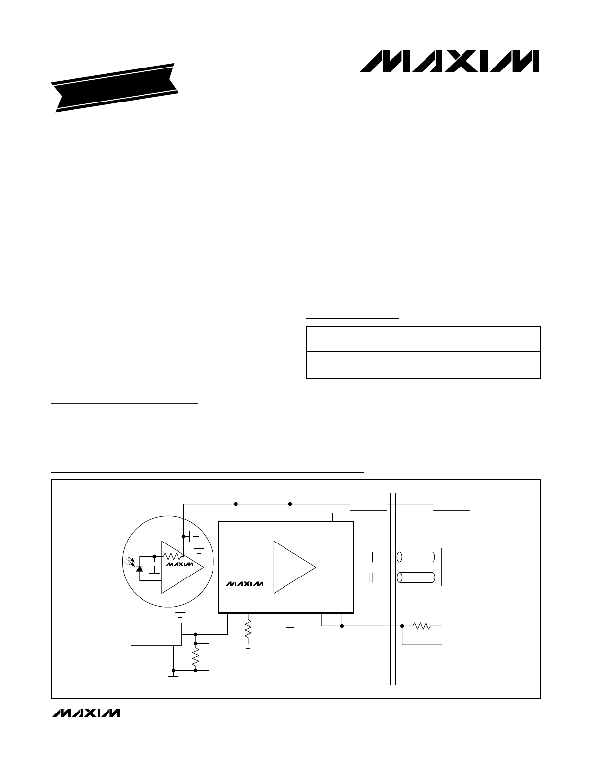
MAX3748/
MAX3748A
MAX3744 TIA*
DS1858
3-INPUT DIAGNOSTIC
MONITOR
R1
3kΩ
C1
0.1µF
IN+
IN-
RSSI TH DISABLE LOS
0.1µF
OUTPOL CAZ1 CAZ2V
CC
GND
4.7kΩ TO 10kΩ
LOS
V
CC
_HOST
OUT+
50Ω
0.1µF
OUT-
50Ω
0.1µF
SERDES
R
TH
SUPPLY FILTER HOST FILTER
V
CC
_RX
4-PIN TO HEADER
HOST BOARDSFP OPTICAL RECEIVER
*FUTURE PRODUCT.
Typical Operating Circuits
19-2717; Rev 1; 7/03
For pricing, delivery, and ordering information, please contact Maxim/Dallas Direct! at
1-888-629-4642, or visit Maxim’s website at www.maxim-ic.com.
EVALUATION KIT
AVAILABLE
*EP = Exposed pad.
Functional Diagram and Pin Configuration appear at end of
data sheet.
Typical Operating Circuits continued at end of data sheet.
PART TEMP RANGE
MAX3748ETE -40°C to +85°C 16 QFN-EP* T1633-3
MAX3748AETE -40°C to +85°C 16 QFN-EP* T1633-3
PINPACKAGE
PACKAGE
CODE

MAX3748/MAX3748A
Compact 155Mbps to 3.2Gbps
Limiting Amplifier
2 _______________________________________________________________________________________
ABSOLUTE MAXIMUM RATINGS
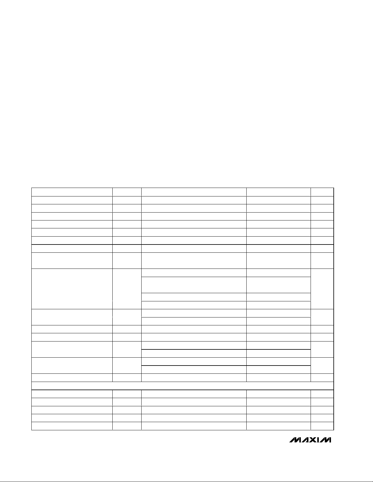
ELECTRICAL CHARACTERISTICS
(VCC= 2.97V to 3.63V, ambient temperature = -40°C to +85°C, CML output load is 50Ω to VCC, CAZ= 0.1µF, typical values are at
+25°C, V
CC
= 3.3V, unless otherwise specified. The data input transition time is controlled by a 4th-order Bessel filter with f
-3dB
=
0.75
✕ 2.667GHz for all data rates of 2.667Gbps and below, and with f
-3dB
= 0.75 ✕ 3.2GHz for a data rate of 3.2Gbps.)
Stresses beyond those listed under “Absolute Maximum Ratings” may cause permanent damage to the device. These are stress ratings only, and functional
operation of the device at these or any other conditions beyond those indicated in the operational sections of the specifications is not implied. Exposure to
absolute maximum rating conditions for extended periods may affect device reliability.
Power-Supply Voltage (VCC).................................-0.5V to +6.0V
Voltage at IN+, IN- ..........................(VCC- 2.4V) to (VCC+ 0.5V)
Voltage at DISABLE, OUTPOL, RSSI,
CAZ1, CAZ2, LOS, TH............................-0.5V to (VCC+ 0.5V)
Current into LOS ...................................................-1mA to +9mA
Differential Input Voltage (IN+ - IN-) .....................................2.5V
Continuous Current at CML Outputs
(OUT+, OUT-) ...............................................-25mA to +25mA
Continuous Power Dissipation (TA= +70°C)
16-Pin QFN (derate 17.7mW above +70°C) ....................1.4W
Operating Junction Temperature Range (T
J
) ....-55°C to +150°C
Storage Ambient Temperature Range (T
s
)........-55°C to +150°C
Single-Ended Input Resistance Single ended to V
Input Return Loss Differential, f < 3GHz, DUT is powered on 13 dB
Input Sensitivity V
Input Overload V
Single-Ended Output Resistance Single ended to V
Output Return Loss Differential, f < 3GHz, DUT is powered on 10 dB
Differential Output Voltage 600 780 1200 mV
Differential Output Signal when
Disabled
Deterministic Jitter
(Notes 2, 3)
Random Jitter
(Note 5)
Data Output Transition Time 20% to 80% (Note 2) 86 115 ps
Input-Referred Noise 185 µV
Low-Frequency Cutoff
Power-Supply Current I
Power-Supply Noise Rejection PSNR f < 2MHz 26 dB
LOSS OF SIGNAL at 2.5Gbps (Notes 2, 7)
LOS Hysteresis 10l og ( V
LOS Assert/Deassert Time (Note 8) 2 100 µs
Low LOS Assert Level RTH = 20kΩ 2.8 4.1 mV
Low LOS Deassert Level RTH = 20kΩ 6.7 11.6 mV
Medium LOS Assert Level RTH = 280Ω 10.3 15.2 mV
PARAMETER SYMBOL CONDITIONS MIN TYP MAX UNITS
IN-MIN
IN-MAX
DJ
CC
(Note 1) 5 mV
(Note 1) 1200 mV
Outputs AC-coupled, V
input (Note 2)
K28.5 pattern at 3.2Gbps 8.5 25
223- 1 PRBS equivalent pattern at 2.7Gbps
(Note 4)
K28.5 pattern at 2.1Gbps 7.8 25
23
2
- 1 PRBS equivalent pattern at 155Mbps 25 50
Input = 5mV
Input = 10mV
CAZ = open 70
= 0.1µF 0.8
C
AZ
(Note 6) 32 49
LOS disabled 37
D E A S S E R T
CC
CC
applied to
IN-MAX
P-P
P-P
/V
) 1.25 2.2 dB
A S S E R T
42 50 58 Ω
42 50 58 Ω
10 mV
9.3 30
6.5
3
ps
ps
kHz
P-P
P-P
P-P
P-P
P-P
RMS
RMS
mA
P-P
P-P
P-P

MAX3748/MAX3748A
Compact 155Mbps to 3.2Gbps
Limiting Amplifier
_______________________________________________________________________________________ 3
Note 1: Between sensitivity and overload, all AC specifications are met.
Note 2: Guaranteed by design and characterization.
Note 3: The deterministic jitter caused by this filter is not included in the DJ generation specifications (input).
Note 4: 2
23
- 1 PRBS pattern was substituted by K28.5 pattern to determine the high-speed portion of the deterministic jitter. The
low-speed portion of the DJ (baseline wander) was obtained by measuring the eye width difference between outputs generated using K28.5 and 2
23
- 1 PRBS patterns.
Note 5: Random jitter was measured without using a filter at the input.
Note 6: The supply current measurement excludes the CML output currents by connecting the CML outputs to a separate V
CC
(see Figure 1).
Note 7: Unless otherwise specified, the pattern for all LOS detect specifications is 2
23
- 1 PRBS.
Note 8: The signal at the input is switched between two amplitudes, Signal_ON and Signal_OFF, as shown in Figure 2.
Note 9: I
CM_INPUT
is the input common mode. I
RSSI
is the current at the RSSI output.
Note 10: Stability is defined as variation over temperature and power supply with respect to the typical gain of the part.
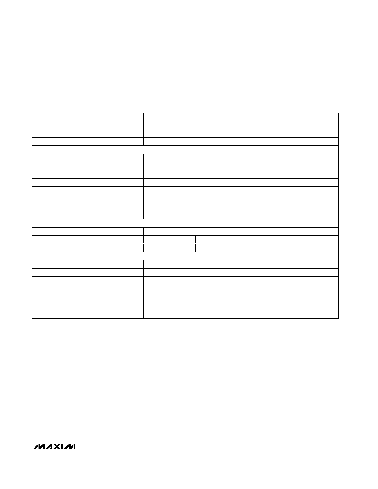
ELECTRICAL CHARACTERISTICS (continued)
(VCC= 2.97V to 3.63V, ambient temperature = -40°C to +85°C, CML output load is 50Ω to VCC, CAZ= 0.1µF, typical values are at
+25°C, V
CC
= 3.3V, unless otherwise specified. The data input transition time is controlled by a 4th-order Bessel filter with f
-3dB
=
0.75
✕ 2.667GHz for all data rates of 2.667Gbps and below, and with f
-3dB
= 0.75 ✕ 3.2GHz for data rate of 3.2Gbps.)
Medium LOS Deassert Level RTH = 280Ω 25 38.6 mV
High LOS Assert Level RTH = 80Ω 22.8 38.3 mV
High LOS Deassert Level RTH = 80Ω 65.2 99.3 mV
LOSS OF SIGNAL at 155Mbps (Note 7)
LOS Hysteresis 10log ( V
LOS Assert/Deassert Time (Note 8) 20 µs
Low LOS Assert Level RTH = 20kΩ 3.5 mV
Low LOS Deassert Level RTH = 20kΩ 5.6 mV
Medium LOS Assert Level RTH = 280Ω 13.3 mV
Medium LOS Deassert Level RTH = 280Ω 21.2 mV
High LOS Assert Level RTH = 80Ω 33.3 mV
High LOS Deassert Level RTH = 80Ω 55.5 mV
RSSI
RSSI Current Gain (Note 9) A
Input-Referred RSSI Current
Stability
TTL/CMOS I/O
LOS Output High Voltage V
LOS Output Low Voltage V
LOS Output Current
DISABLE Input High V
DISABLE Input Low V
DISABLE Input Current R
PARAMETER SYMBOL CONDITIONS MIN TYP MAX UNITS
D E A S S E R T
A
RSSI
= I
RSSI
I
RSSI/ARSSI
RSSI/ICM_RSSI
(Note 10)
R
OH
OL
= 4.7kΩ to10kΩ to V
LOS
R
= 4.7kΩ to10kΩ to V
LOS
R
= 4.7kΩ to10kΩ to V
LOS
IC is powered down
IH
IL
= 4.7kΩ to 10kΩ to V
LOS
/V
) 2.1 dB
A S S E R T
I
CM_INPUT
I
CM_INPUT
< 6.6mA -31 +33
> 6.6mA -73 +90
(3V) 2.4 V
CC_host
(3.6V) 0.4 V
CC_host
(3.3V);
CC_host
2.0 V
CC_host
0.03
40 µA
0.8 V
10 µA
P-P
P-P
P-P
P-P
P-P
P-P
P-P
P-P
P-P
µA

MAX3748/MAX3748A
Compact 155Mbps to 3.2Gbps
Limiting Amplifier
4 _______________________________________________________________________________________
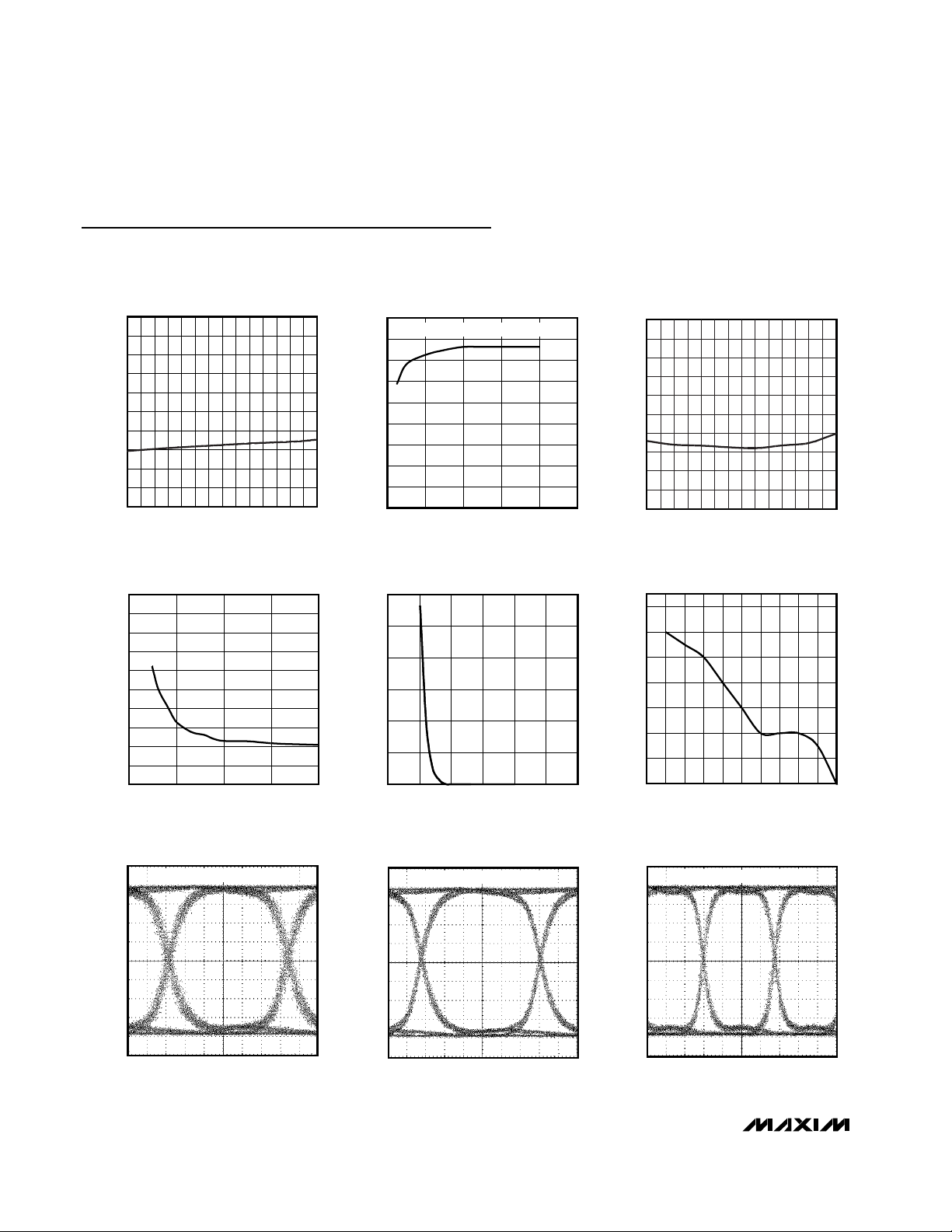
Typical Operating Characteristics
(TA= +25°C and VCC= +3.3V, unless otherwise specified.)
SUPPLY CURRENT
vs. TEMPERATURE
MAX3748 toc01
TEMPERATURE (°C)
CURRENT (mA)
908060 70-10 0 10 20 30 40 50-30-20
10
20
30
40
50
60
70
80
90
100
0
-40 100
TRANSFER FUNCTION
MAX3748 toc02
DIFFERENTIAL INPUT (mV
P-P
)
DIFFERENTIAL OUTPUT (mV
P-P
)
5432
100
200
300
400
500
600
700
800
900
0
16
OUTPUT VOLTAGE vs. INPUT VOLTAGE
RANDOM JITTER vs. TEMPERATURE
(INPUT LEVEL 10mV
P-P
)
MAX3748 toc03
TEMPERATURE (°C)
RANDOM JITTER (ps
RMS
)
9080706050403020100-10-20-30
2
4
3
1
6
8
9
7
5
10
0
-40 100
RANDOM JITTER
vs. INPUT AMPLITUDE
MAX3748 toc04
DIFFERENTIAL INPUT AMPLITUDE (mV
P-P
)
RANDOM JITTER (ps
RMS
)
302010
1
2
3
4
5
6
7
8
9
10
0
040
BIT-ERROR RATIO vs. INPUT VOLTAGE
MAX3748 toc05
INPUT VOLTAGE (mV
P-P
)
BIT-ERROR RATIO (10
-12
)
4.54.03.53.02.5
200
400
600
800
1000
1200
0
2.0 5.0
DETERMINISTIC JITTER vs. INPUT
COMMON-MODE VOLTAGE (V
CC
TO V
CC
- 0.8V)
MAX3748 toc06
COMMON-MODE VOLTAGE (VCC + x)
DETERMINISTIC JITTER (ps
P-P
)
-0.1-0.2-0.3-0.4-0.5-0.6-0.7-0.8-0.9
12
14
16
18
20
22
24
10
-1.0 0
OUTPUT EYE DIAGRAM (MINIMUM INPUT)
MAX3748 toc07
50ps/div
100mV/div
3.2Gbps, 223 - 1 PRBS, 5mV
P-P
OUTPUT EYE DIAGRAM (MAXIMUM INPUT)
MAX3748 toc08
50ps/div
100mV/div
3.2Gbps, 223 - 1 PRBS, 1200mV
P-P
OUTPUT EYE DIAGRAM (MINIMUM INPUT)
MAX3748 toc09
100ps/div
100mV/div
2.7Gbps, 223 - 1 PRBS, 5mV
P-P
 Loading...