

General Description
The MAX3748/MAX3748A multirate limiting amplifier functions as a data quantizer for SONET, Fibre Channel, and
Gigabit Ethernet optical receivers. The amplifier accepts
a wide range of input voltages and provides constantlevel current-mode logic (CML) output voltages with controlled edge speeds.
A received-signal-strength indicator (RSSI) is available
when the MAX3748/MAX3748A is combined with the
MAX3744 SFP transimpedance amplifier (TIA). A receiver
consisting of the MAX3744 and the MAX3748/ MAX3748A
can provide up to 19dB RSSI dynamic range. Additional
features include a programmable loss-of-signal (LOS)
detect, an optional disable function (DISABLE), and an
output signal polarity reversal (OUTPOL). Output disable
can be used to implement squelch.
The combination of the MAX3748/MAX3748A and the
MAX3744 allows for the implementation of all the smallform-factor SFF-8472 digital diagnostic specifications
using a standard 4-pin TO-46 header. The MAX3748/
MAX3748A is packaged in a 3mm ✕ 3mm 16-pin thin QFN
package with an exposed pad.
Applications
Gigabit Ethernet SFF/SFP Transceiver Modules
Fibre Channel SFF/SFP Transceiver Modules
Multirate OC-3 to OC-48-FEC SFF/SFP
Transceiver Modules
Features
♦ SFP Reference Design Available
♦ 16-Pin QFN Package with 3mm
✕ 3mm Footprint
♦ Single +3.3V Supply Voltage
♦ 86ps Rise and Fall Time
♦ Loss of Signal with Programmable Threshold
♦ RSSI Interface (with MAX3744 TIA)
♦ Output Disable
♦ Polarity Select
♦ 8.5ps
P-P
Deterministic Jitter (4.25Gbps)
MAX3748/MAX3748A
Compact 155Mbps to 4.25Gbps
Limiting Amplifier
________________________________________________________________ Maxim Integrated Products 1
Ordering Information
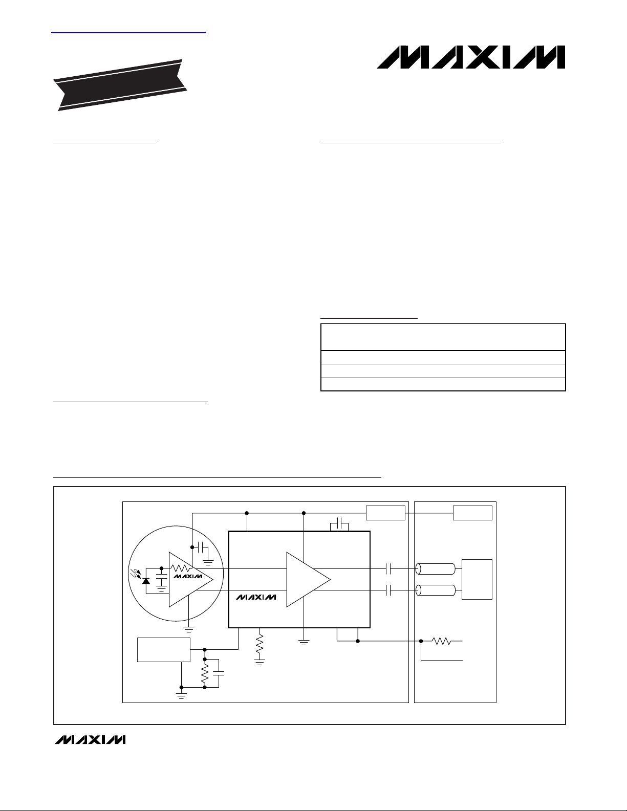
MAX3748/
MAX3748A
MAX3744 TIA
DS1858
3-INPUT DIAGNOSTIC
MONITOR
R1
3kΩ
C1
0.1µF
IN+
IN-
RSSI TH DISABLE LOS
0.1µF
OUTPOL CAZ1 CAZ2V
CC
GND
4.7kΩ TO 10kΩ
LOS
V
CC
_HOST
OUT+
50Ω
0.1µF
OUT-
50Ω
0.1µF
SERDES
R
TH
SUPPLY FILTER HOST FILTER
V
CC
_RX
4-PIN TO HEADER
HOST BOARDSFP OPTICAL RECEIVER
Typical Operating Circuits
19-2717; Rev 3; 8/05
For pricing, delivery, and ordering information, please contact Maxim/Dallas Direct! at
1-888-629-4642, or visit Maxim’s website at www.maxim-ic.com.
EVALUATION KIT
AVAILABLE
PART
TEMP RANGE
PIN-
PKG
CODE
MAX3748HETE*
16 TQFN
T1633FH-3
MAX3748ETE
16 TQFN T1633F-3
MAX3748AETE
16 TQFN T1633F-3
*MAX3748A device in a hybrid lead-free package. See the
Detailed Description for more information.
Functional Diagram and Pin Configuration appear at end of
data sheet.
Typical Operating Circuits continued at end of data sheet.
查询MAX3747AEVKIT供应商
-40°C to +85°C
-40°C to +85°C
-40°C to +85°C
PACKAGE
MAX3748/MAX3748A
Compact 155Mbps to 4.25Gbps
Limiting Amplifier
2 _______________________________________________________________________________________
ABSOLUTE MAXIMUM RATINGS
ELECTRICAL CHARACTERISTICS
(VCC= 2.97V to 3.63V, ambient temperature = -40°C to +85°C, CML output load is 50Ω to VCC, CAZ= 0.1µF, typical values are at
+25°C, V
CC
= 3.3V, unless otherwise specified. The data input transition time is controlled by a 4th-order Bessel filter with f
-3dB
=
0.75
✕ 2.667GHz for all data rates of 2.667Gbps and below, and with f
-3dB
= 0.75 ✕ 3.2GHz for a data rate of 3.2Gbps. No input filter
for 4.25Gbps specifications.)
Stresses beyond those listed under “Absolute Maximum Ratings” may cause permanent damage to the device. These are stress ratings only, and functional
operation of the device at these or any other conditions beyond those indicated in the operational sections of the specifications is not implied. Exposure to
absolute maximum rating conditions for extended periods may affect device reliability.
Power-Supply Voltage (VCC).................................-0.5V to +6.0V
Voltage at IN+, IN- ..........................(V
CC
- 2.4V) to (VCC+ 0.5V)
Voltage at DISABLE, OUTPOL, RSSI,
CAZ1, CAZ2, LOS, TH............................-0.5V to (V
CC
+ 0.5V)
Current into LOS ...................................................-1mA to +9mA
Differential Input Voltage (IN+ - IN-) .....................................2.5V
Continuous Current at CML Outputs
(OUT+, OUT-) ...............................................-25mA to +25mA
Continuous Power Dissipation (T
A
= +70°C)
16-Pin QFN (derate 17.7mW above +70°C) ....................1.4W
Operating Junction Temperature Range (TJ) ....-55°C to +150°C
Storage Ambient Temperature Range (Ts)........-55°C to +150°C
PARAMETER
CONDITIONS
UNITS
Single-Ended Input Resistance Single ended to V
CC
42 50 58 Ω
Input Return Loss Differential, f < 3GHz, DUT is powered on 13 dB
Input Sensitivity
(Note 1) 5
mV
P-P
Input Overload
(Note 1)
mV
P-P
Single-Ended Output Resistance
Single ended to V
CC
42 50 58 Ω
Output Return Loss Differential, f < 3GHz, DUT is powered on 10 dB
Differential Output Voltage
mV
P-P
Differential Output Signal when
Disabled
Outputs AC-coupled, V
IN-MAX
applied to
input (Note 2)
10
mV
P-P
K28.5 pattern at 4.25Gbps 8.7 25
K28.5 pattern at 3.2Gbps 8.5 25
223- 1 PRBS equivalent pattern at 2.7Gbps
(Note 4)
9.3 30
K28.5 pattern at 2.1Gbps 7.8 25
Deterministic Jitter
(Notes 2, 3)
DJ
25 50
ps
P-P
Input = 5mV
P-P
6.5
Random Jitter
(Note 5)
Input = 10mV
P-P
3
ps
RMS
20% to 80%, 4.25Gbps
3.1875GHz Bessel input filter
V
IN
= 20mV
P-P
60
Data Output Transition Time
20% to 80% (Note 2) 86 115
ps
Input-Referred Noise
µV
RMS
CAZ = open 70
Low-Frequency Cutoff
C
AZ
= 0.1µF 0.8
kHz
(Note 6) 32 49
Power-Supply Current I
CC
LOS disabled 37
mA
Power-Supply Noise Rejection PSNR f < 2MHz 26 dB
LOSS OF SIGNAL at 4.25Gbps K28.5 pattern (Note 2)
LOS Hysteresis 10l og ( V
D E A S S E R T
/V
A S S E R T
)
2.2 dB
LOS Assert/Deassert Time (Note 8) 2 100 µs
LOS Assert RTH = 280kΩ
mV
P-P
LOS Deassert RTH = 280kΩ 28
mV
P-P
SYMBOL
V
IN-MIN
V
IN-MAX
MIN TYP MAX
1200
223- 1 PRBS equivalent pattern at 155Mbps
600 780 1200
1.25
185
18.5
MAX3748/MAX3748A
Compact 155Mbps to 4.25Gbps
Limiting Amplifier
_______________________________________________________________________________________ 3
Note 1: Between sensitivity and overload, all AC specifications are met.
Note 2: Guaranteed by design and characterization.
Note 3: The deterministic jitter caused by this filter is not included in the DJ generation specifications (input).
Note 4: 2
23
- 1 PRBS pattern was substituted by K28.5 pattern to determine the high-speed portion of the deterministic jitter. The
low-speed portion of the DJ (baseline wander) was obtained by measuring the eye width difference between outputs generated using K28.5 and 2
23
- 1 PRBS patterns.
Note 5: Random jitter was measured without using a filter at the input.
Note 6: The supply current measurement excludes the CML output currents by connecting the CML outputs to a separate V
CC
(see Figure 1).
Note 7: Unless otherwise specified, the pattern for all LOS detect specifications is 2
23
- 1 PRBS.
Note 8: The signal at the input is switched between two amplitudes, Signal_ON and Signal_OFF, as shown in Figure 2.
Note 9: I
CM_INPUT
is the input common mode. I
RSSI
is the current at the RSSI output.
Note 10: Stability is defined as variation over temperature and power supply with respect to the typical gain of the part.
ELECTRICAL CHARACTERISTICS (continued)
(VCC= 2.97V to 3.63V, ambient temperature = -40°C to +85°C, CML output load is 50Ω to VCC, CAZ= 0.1µF, typical values are at
+25°C, V
CC
= 3.3V, unless otherwise specified. The data input transition time is controlled by a 4th-order Bessel filter with f
-3dB
=
0.75
✕ 2.667GHz for all data rates of 2.667Gbps and below, and with f
-3dB
= 0.75 ✕ 3.2GHz for a data rate of 3.2Gbps. No input filter
for 4.25Gbps specifications.)
PARAMETER
SYMBOL
CONDITIONS
MIN
TYP
MAX
UNITS
LOSS OF SIGNAL at 2.5Gbps (Notes 2, 7)
LOS Hysteresis 10l og ( V
D E A S S E R T
/V
A S S E R T
)
2.2 dB
LOS Assert/Deassert Time (Note 8) 2 100 µs
Low LOS Assert Level RTH = 20kΩ 2.8 4.1
mV
P-P
Low LOS Deassert Level RTH = 20kΩ 6.7
mV
P-P
Medium LOS Assert Level RTH = 280Ω
mV
P-P
Medium LOS Deassert Level RTH = 280Ω 25
mV
P-P
High LOS Assert Level RTH = 80Ω
mV
P-P
High LOS Deassert Level RTH = 80Ω
mV
P-P
LOSS OF SIGNAL at 155Mbps (Note 7)
LOS Hysteresis 10log ( V
D E A S S E R T
/V
A S S E R T
) 2.1 dB
LOS Assert/Deassert Time (Note 8) 20 µs
Low LOS Assert Level RTH = 20kΩ 3.5
mV
P-P
Low LOS Deassert Level RTH = 20kΩ 5.6
mV
P-P
Medium LOS Assert Level RTH = 280Ω
mV
P-P
Medium LOS Deassert Level RTH = 280Ω
mV
P-P
High LOS Assert Level RTH = 80Ω
mV
P-P
High LOS Deassert Level RTH = 80Ω
mV
P-P
RSSI
RSSI Current Gain (Note 9) A
RSSI
A
RSSI
= I
RSSI/ICM_RSSI
I
CM_INPUT
< 6.6mA -31 +33
Input-Referred RSSI Current
Stability
I
RSSI/ARSSI
(Note 10)
I
CM_INPUT
> 6.6mA -73 +90
µA
TTL/CMOS I/O
LOS Output High Voltage V
OH
R
LOS
= 4.7kΩ to10kΩ to V
CC_host
(3V) 2.4 V
LOS Output Low Voltage V
OL
R
LOS
= 4.7kΩ to10kΩ to V
CC_host
(3.6V) 0.4 V
LOS Output Current
R
LOS
= 4.7kΩ to10kΩ to V
CC_host
(3.3V);
IC is powered down
40 µA
DISABLE Input High V
IH
2.0 V
DISABLE Input Low V
IL
0.8 V
DISABLE Input Current R
LOS
= 4.7kΩ to 10kΩ to V
CC_host
10 µA
1.25
10.3 15.2
22.8 38.3
65.2 99.3
13.3
21.2
33.3
55.5
0.03
11.6
38.6
MAX3748/MAX3748A
Compact 155Mbps to 4.25Gbps
Limiting Amplifier
4 _______________________________________________________________________________________
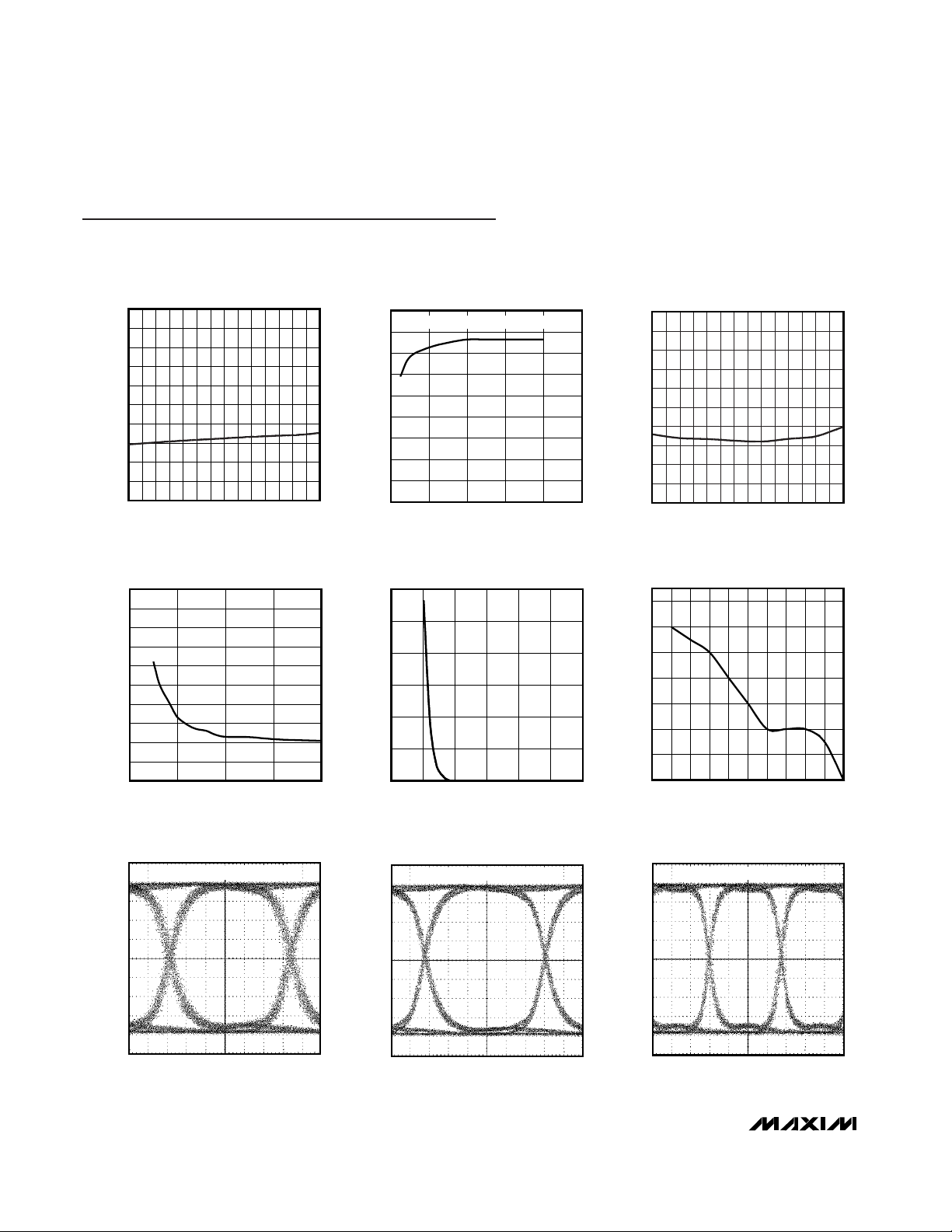
Typical Operating Characteristics
(TA= +25°C and VCC= +3.3V, unless otherwise specified.)
SUPPLY CURRENT
vs. TEMPERATURE
MAX3748 toc01
TEMPERATURE (°C)
CURRENT (mA)
908060 70-10 0 10 20 30 40 50-30-20
10
20
30
40
50
60
70
80
90
100
0
-40 100
TRANSFER FUNCTION
MAX3748 toc02
DIFFERENTIAL INPUT (mV
P-P
)
DIFFERENTIAL OUTPUT (mV
P-P
)
5432
100
200
300
400
500
600
700
800
900
0
16
OUTPUT VOLTAGE vs. INPUT VOLTAGE
RANDOM JITTER vs. TEMPERATURE
(INPUT LEVEL 10mV
P-P
)
MAX3748 toc03
TEMPERATURE (°C)
RANDOM JITTER (ps
RMS
)
9080706050403020100-10-20-30
2
4
3
1
6
8
9
7
5
10
0
-40 100
RANDOM JITTER
vs. INPUT AMPLITUDE
MAX3748 toc04
DIFFERENTIAL INPUT AMPLITUDE (mV
P-P
)
RANDOM JITTER (ps
RMS
)
302010
1
2
3
4
5
6
7
8
9
10
0
040
BIT-ERROR RATIO vs. INPUT VOLTAGE
MAX3748 toc05
INPUT VOLTAGE (mV
P-P
)
BIT-ERROR RATIO (10
-12
)
4.54.03.53.02.5
200
400
600
800
1000
1200
0
2.0 5.0
DETERMINISTIC JITTER vs. INPUT
COMMON-MODE VOLTAGE (V
CC
TO V
CC
- 0.8V)
MAX3748 toc06
COMMON-MODE VOLTAGE (VCC + x)
DETERMINISTIC JITTER (ps
P-P
)
-0.1-0.2-0.3-0.4-0.5-0.6-0.7-0.8-0.9
12
14
16
18
20
22
24
10
-1.0 0
OUTPUT EYE DIAGRAM (MINIMUM INPUT)
MAX3748 toc07
50ps/div
100mV/div
3.2Gbps, 223 - 1 PRBS, 5mV
P-P
OUTPUT EYE DIAGRAM (MAXIMUM INPUT)
MAX3748 toc08
50ps/div
100mV/div
3.2Gbps, 223 - 1 PRBS, 1200mV
P-P
OUTPUT EYE DIAGRAM (MINIMUM INPUT)
MAX3748 toc09
100ps/div
100mV/div
2.7Gbps, 223 - 1 PRBS, 5mV
P-P

MAX3748/MAX3748A
Compact 155Mbps to 4.25Gbps
Limiting Amplifier
_______________________________________________________________________________________ 5
OUTPUT EYE DIAGRAM WITH MAXIMUM INPUT
(DATA RATE OF 2.6667Gbps)
MAX3748 toc10
50ps/div
100mV/div
2.7Gbps, 223 - 1 PRBS, 1200mV
P-P
OUTPUT EYE DIAGRAM AT +100°C
(MINIMUM INPUT)
MAX3748 toc11
50ps/div
100mV/div
3.2Gbps, 223 - 1 PRBS, 5mV
P-P
ASSERT/DEASSERT LEVELS vs. R
TH
MAX3748 toc12
RTH (kΩ)
ASSERT/DEASSERT (mV
P-P
)
0.1
1
10
10
100
1
0.01 100
ASSERT
DEASSERT
INPUT RETURN GAIN vs. FREQUENCY (SDD11)
(INPUT SIGNAL LEVEL = -40dBm)
MAX3748 toc13
FREQUENCY (Hz)
GAIN (dB)
1G
-30
-20
-10
0
10
20
30
-40
100M 10G
OUTPUT
DISABLED
OUTPUT RETURN GAIN vs. FREQUENCY (SDD22)
(INPUT SIGNAL LEVEL = -40dBm)
MAX3748 toc14
FREQUENCY (Hz)
GAIN (dB)
1G
-30
-20
-10
0
10
20
30
-40
100M 10G
DETERMINISTIC JITTER vs. INPUT OFFSET VOLTAGE
(2.667Gbps, K28.5)
MAX3748 toc15
INPUT OFFSET VOLTAGE (mV
P-P
)
DETERMINISTIC JITTER (ps
P-P
)
420-2-4
2
4
6
8
10
12
14
16
18
20
0
-6 6
LOS HYSTERESIS vs. TEMPERATURE
(2.667bps, 2
10
- 1 PRBS)
MAX3748 toc16
TEMPERATURE (°C)
10LOG (DEASSERT/ASSERT) (dB)
9080706050403020100-10-20-30
1
2
3
4
5
6
0
-40 100
RTH = 20kΩ
RTH = 80Ω
RTH = 280Ω
0
200
100
400
300
600
500
700
0 400200 600 800100 500300 700 900 1000
RSSI CURRENT GAIN vs. INPUT TIA CURRENT
(MAX3744 AND MAX3748)
MAX3748 toc17
INPUT TIA CURRENT (µA)
OUTPUT RSSI CURRENT (µA)
Typical Operating Characteristics (continued)
(TA= +25°C and VCC= +3.3V, unless otherwise specified.)

MAX3748/MAX3748A
Detailed Description
The limiting amplifier consists of an input buffer, a multistage amplifier, offset correction circuitry, an output
buffer, power-detection circuitry, and signal-detect circuitry (see Functional Diagram).
Input Buffer
The input buffer is shown in Figure 3. It provides 50Ω
termination for each input signal IN+ and IN-. The
MAX3748/MAX3748A can be DC- or AC-coupled to a
TIA (TIA output offset degrades receiver performance if
DC-coupled). The CML input buffer is optimized for the
MAX3744 TIA.
Gain Stage
The high-bandwidth gain stage provides approximately
53dB of gain.
Compact 155Mbps to 4.25Gbps
Limiting Amplifier
6 _______________________________________________________________________________________
Pin Description
PIN NAME FUNCTION
1, 4, 12 V
CC
Supply Voltage
2 IN+ Noninverted Input Signal, CML
3 IN- Inverted Input Signal, CML
5TH
Loss-of-Signal Threshold Pin. Resistor to ground (R
TH
) sets the LOS threshold. Connecting this pin to
V
CC
disables the LOS circuitry and reduces power consumption.
6
Disable Input, CMOS/TTL. The data outputs are held static when this pin is asserted high. The LOS
function remains active when the outputs are disabled, CMOS. On the MAX3748, this pin does not
include ESD protection. If routed through the DS1858/DS1859 controller IC, no additional ESD protection
is required. On the MAX3748A, this pin has ESD protection.
7 LOS
Noninverted Loss-of-Signal Output. LOS is asserted high when the signal drops below the assert
threshold set by the TH input. The output is open collector (Figure 5). On the MAX3748, this pin does not
include ESD protection. If routed through the DS1858/DS1859 controller IC, no additional ESD protection
is required. On the MAX3748A, this pin has ESD protection.
8, 16 GND Supply Ground
9
Output Polarity Control Input. Connect to GND for an inversion of polarity through the limiting amplifier
and connect to V
CC
for normal operation.
10 OUT- Inverted Data Output, CML
11 OUT+ Noninverted Data Output, CML
13 RSSI
Received-Signal-Strength Indicator. This current output can be used to obtain a ground-referenced
voltage proportional to photodiode current with the MAX3744 by connecting an external resistor between
this pin and GND.
14 CAZ2
Offset Correction Loop Capacitor Connection. A capacitor connected between this pin and CAZ1
extends the time constant of the offset correction loop. Typical value of CAZ is 0.1µF. The offset
correction is disabled when the CAZ1 and CAZ2 pins are shorted together.
15 CAZ1
O ffset C or r ecti on Loop C ap aci tor C onnecti on. A cap aci tor connected b etw een thi s p i n and C AZ 2 extend s
the ti m e constant of the offset cor r ecti on l oop . Typ i cal val ue of C
A Z
i s 0.1µF. The offset cor r ecti on i s d i sab l ed
w hen the C AZ 1 and C AZ 2 p i ns ar e shor ted tog ether .
EP
Exposed
paddle
Connect the exposed paddle to board ground for optimal electrical and thermal performance.
Figure 1. Power-Supply Current Measurement
DISABLE
OUTPOL
V
CC
I
(SUPPLY CURRENT)
CC
50Ω
MAX3748/
MAX3748A
50Ω
I
(CML
OUT
OUTPUT CURRENT)
R
TH

Offset Correction Loop
The MAX3748/MAX3748A is susceptible to DC offsets
in the signal path because it has high gain. In communication systems using NRZ data with a 50% duty
cycle, pulse-width distortion present in the signal or
generated in the transimpedance amplifier appears as
an input offset and is reduced by the offset correction
loop. For Gigabit Ethernet and Fibre Channel applications, no capacitor is required. For SONET applications,
CAZ= 0.1µF is recommended. This capacitor determines the lower 3dB frequency of the data path.
CML Output Buffer
The MAX3748/MAX3748A limiting amplifier’s CML output provides high tolerance to impedance mismatches
and inductive connectors. The output current is approximately 18mA. The output is disabled by connecting the
DISABLE pin to VCC. If the LOS pin is connected to the
DISABLE pin, the outputs OUT+ and OUT- are at a static voltage (squelch) whenever the input signal level
drops below the LOS threshold. The output buffer can
be AC- or DC-coupled to the load (Figure 4).
Power-Detect and
Loss-of-Signal Indicator
The MAX3748/MAX3748A is equipped with an LOS circuitry, which indicates when the input signal is below a
programmable threshold, set by resistor R
TH
at the TH
pin (see Typical Operating Characteristics for appropriate
resistor sizing). An averaging peak-power detector compares the input signal amplitude with this threshold and
feeds the signal detect information to the LOS output,
which is open collector. Two control voltages, V
ASSERT
and V
DEASSERT
, define the LOS assert and deassert lev-
els. To prevent LOS chatter in the region of the programmed threshold, approximately 2dB of hysteresis is
built into the LOS assert/deassert function. Once asserted, LOS is not deasserted until the input amplitude rises
to the required level (V
DEASSERT
) (Figure 5).
Hybrid Lead-Free Package
The MAX3748HETE is a MAX3748A in a hybrid leadfree package. It is a hybrid part, which contains highlead bumps inside a lead-free thin QFN package. The
part is not 100% lead-free; however, the high-lead solder in the internal portion of the part does meet the
RoHS exemption for high-lead solders. For more information, visit www.maxim-ic.com/emmi/.
MAX3748/MAX3748A
Compact 155Mbps to 4.25Gbps
Limiting Amplifier
_______________________________________________________________________________________________________ 7
1dB
6dB
0V
SIGNAL ON
MAX DEASSERT LEVEL
MIN DEASSERT LEVEL
POWER-DETECT WINDOW
V
IN
TIME
SIGNAL OFF
Figure 2. LOS Deassert Threshold Set 1dB Below the Minimum
by Receiver Sensitivity (for Selected R
TH
)
50Ω 50Ω
75kΩ
IN+
IN-
0.25pF
0.25pF
V
CC
ESD
STRUCTURES
Figure 3. CML Input Buffer
Q3 Q4 Q1
V
CC
50Ω50Ω
Q2
18mA 18mA
DISABLE
DISABLE
DISABLE
DATA
OUT+
OUT-
ESD
STRUCTURES
Figure 4. CML Output Buffer

MAX3748/MAX3748A
Design Procedure
Program the LOS Assert Threshold
External resistor RTHprograms the LOS threshold. See
the Assert/Deassert Levels vs. R
TH
graph in the Typical
Operating Characteristics to select the appropriate
resistor.
Select the Coupling Capacitor
When AC-coupling is desired, coupling capacitors C
IN
and C
OUT
should be selected to minimize the receiver’s
deterministic jitter. Jitter is decreased as the input lowfrequency cutoff (fIN) is decreased:
fIN= 1 / [2π(50)(CIN)]
For ATM/SONET or other applications using scrambled
NRZ data, select (CIN, C
OUT
) ≥ 0.1µF, which provides
fIN< 32kHz. For Fibre Channel, Gigabit Ethernet, or
other applications using 8B/10B data coding, select
(CIN, C
OUT
) ≥ 0.01µF, which provides fIN< 320kHz.
Refer to Application Note HFAN-1.1: Choosing AC-
Coupling Capacitors.
Select the Offset-Correction Capacitor
The capacitor between CAZ1 and CAZ2 determines the
time constant of the signal path DC offset cancellation
loop. To maintain stability, it is important to keep a onedecade separation between fINand the low-frequency
cutoff (fOC) associated with the DC offset cancellation
circuit. For ATM/SONET or other applications using
scrambled NRZ data, fIN< 32kHz, so f
OCMAX
< 3.2kHz.
Therefore, CAZ= 0.1µF (fOC= 2kHz). For Fibre Channel
or Gigabit Ethernet applications, leave pins CAZ1 and
CAZ2 open.
RSSI Implementation
The SFF-8472 Digital Diagnostic specification requires
monitoring of input receive power. The MAX3748/
MAX3748A and MAX3744 receiver chipset allows for
the monitoring of the average receive power by measuring the average DC current of the photodiode.
The MAX3744 preamp measures the average photodiode current and provides the information to the output
common mode. The MAX3748/MAX3748A RSSI detect
block senses the common-mode DC level of input signals IN+ and IN- and provides a ground-referenced output signal (RSSI) proportional to the photodiode current.
The advantage of this implementation is that it allows the
TIA to be packaged in a low-cost conventional 4-pin TO46 header.
The MAX3748/MAX3748A RSSI output is connected to
an analog input channel of the DS1858/DS1859 SFP
controller to convert the analog information into a 16-bit
word. The DS1858/DS1859 provide the receive-power
information to the host board of the optical receiver
through a 2-wire interface. The DS1859 allows for internal
calibration of the receive-power monitor.
The MAX3744 and the MAX3748/MAX3748A have been
optimized to achieve RSSI stability of 2.5dB within the
range of 6µA to 500µA of average input photodiode
current. To achieve the best accuracy, Maxim recommends receive power calibration at the low end (6µA)
and the high end (500µA) of the required range; see
the RSSI Current Gain graph in the Typical Operating
Characteristics.
Connecting to the DS1858/DS1859
For best use of the RSSI monitor, capacitor C1 and
resistor R1 shown in the first Typical Application Circuit
need to be placed as close as possible to the Dallas
diagnostic monitor with the ground of C1 and R1 the
same as the DS1858/DS1859 ground. Capacitor C1
suppresses system noise on the RSSI signal. R1 = 3kΩ
and C1 = 0.1µF is recommended.
Compact 155Mbps to 4.25Gbps
Limiting Amplifier
8 _______________________________________________________________________________________
GND
ESD
STRUCTURE
V
CC
LOS
Figure 5. MAX3748 LOS Output Circuit
GND
ESD
STRUCTURE
V
CC
LOS
Figure 6. MAX3748A LOS Output Circuit

MAX3748/MAX3748A
Compact 155Mbps to 4.25Gbps
Limiting Amplifier
_______________________________________________________________________________________ 9
MAX3744 TIA
DS1858
3-INPUT DIAGNOSTIC
MONITOR
R1
3kΩ
C1
0.1µF
IN+
IN-
RSSI TH DISABLE LOS
0.1µF
OUTPOL CAZ1 CAZ2V
CC
GND
4.7kΩ TO 10kΩ
V
CC_HOST
LOS
OUT+
50Ω
0.1µF
OUT-
50Ω
0.1µF
SERDES
R
TH
SUPPLY FILTER HOST FILTER
V
CC_RX
5-PIN TO HEADER
HOST BOARDSFP OPTICAL RECEIVER
PIN OR
APD
V
CC
(+3.3V OR APD
REFERENCE VOLTAGE)
VCC (+3.3V)
MAX3748/
MAX3748A
Typical Operating Circuits (continued)
MAX3744 TIA
DS1858
3-INPUT DIAGNOSTIC
MONITOR
IN+
IN-
RSSI TH DISABLE LOS
0.1µF
OUTPOL CAZ1 CAZ2V
CC
GND
4.7kΩ TO 10kΩ
V
CC_HOST
LOS
OUT+
50Ω
OUT-
50Ω
C
IN
0.1µF
C
OUT
0.1µF
C
OUT
0.1µF
C
IN
0.1µF
SERDES
R
TH
SUPPLY FILTER HOST FILTER
V
CC_RX
5-PIN TO HEADER
HOST BOARDSFP OPTICAL RECEIVER
PIN OR
APD
V
CC
(+3.3V OR APD
REFERENCE VOLTAGE)
VCC (+3.3V)
HIGH-SIDE
CURRENT SENSE
MAX3748/
MAX3748A

MAX3748/MAX3748A
Compact 155Mbps to 4.25Gbps
Limiting Amplifier
10 ______________________________________________________________________________________
Chip Information
TRANSISTOR COUNT: 1468
PROCESS: SiGe Bipolar
12
13
14
15
16
V
CC
RSSI
CAZ2
CAZ1
GND
GND
LOS
DISABLE
TH
11
OUT+10OUT-
9
1 2 3 4
8
7
6
5
OUTPOL
V
CC
IN+ IN- V
CC
3mm x 3mm TQFN
MAX3748/
MAX3748A
Pin Configuration
50Ω 50Ω
OUTOUT+
V
CC
50Ω 50Ω
V
CC
18mA
DISABLE
OFFSET
CORRECTION
CAZ1 CAZ2
C
AZ
RSSI
DETECT
POWER
DETECT
RSSI
IN-
IN+
TH LOS OUTPOL
MAX3748/
MAX3748A
Functional Diagram

MAX3748/MAX3748A
Compact 155Mbps to 4.25Gbps
Limiting Amplifier
Maxim cannot assume responsibility for use of any circuitry other than circuitry entirely embodied in a Maxim product. No circuit patent licenses are
implied. Maxim reserves the right to change the circuitry and specifications without notice at any time.
Maxim Integrated Products, 120 San Gabriel Drive, Sunnyvale, CA 94086 408-737-7600 ____________________ 11
© 2005 Maxim Integrated Products Printed USA is a registered trademark of Maxim Integrated Products, Inc.
Package Information
(The package drawing(s) in this data sheet may not reflect the most current specifications. For the latest package outline information,
go to www.maxim-ic.com/packages
.)
12x16L QFN THIN.EPS
0.10 C 0.08 C
0.10 M C A B
D
D/2
E/2
E
A1
A2
A
E2
E2/2
L
k
e
(ND - 1) X e
(NE - 1) X e
D2
D2/2
b
L
e
L
C
L
e
C
L
L
C
L
C
PACKAGE OUTLINE
21-0136
2
1
F
12, 16L THIN QFN, 3x3x0.8mm
MARKING
AAAA
1. DIMENSIONING & TOLERANCING CONFORM TO ASME Y14.5M-1994.
EXPOSED PAD VARIATIONS
1.10T1633-1 0.95
CODES
PKG.
T1233-1
MIN.
0.95
NOM.
1.10
D2
1.251.100.951.25
NOM.
1.10
MAX.
1.25
MIN.
0.95
MAX.
1.25
E2
12
N
k
A2
0.25
NE
A1ND0
0.20 REF
-
-
3
0.0230.05
L
e
E
0.45
2.90
b
D
A
0.20
2.90
0.70
0.50 BSC.
0.55
3.00
0.65
3.10
0.25
3.00
0.75
0.30
3.10
0.80
16
0.20 REF
0.25
-
040.02
4
-
0.05
0.50 BSC.
0.30
2.90
0.40
3.00
0.20
2.90
0.70
0.25
3.00
0.75
3.10
0.50
0.80
3.10
0.30
PKG
REF. MIN.
12L 3x3
NOM. MAX. NOM.
16L 3x3
MIN. MAX.
0.35 x 45°
PIN ID
JEDEC
WEED-1
0.35 x 45° WEED-2
2. ALL DIMENSIONS ARE IN MILLIMETERS. ANGLES ARE IN DEGREES.
3. N IS THE TOTAL NUMBER OF TERMINALS.
4. THE TERMINAL #1 IDENTIFIER AND TERMINAL NUMBERING CONVENTION SHALL CONFORM TO
JESD 95-1 SPP-012. DETAILS OF TERMINAL #1 IDENTIFIER ARE OPTIONAL, BUT MUST BE LOCATED
WITHIN THE ZONE INDICATED. THE TERMINAL #1 IDENTIFIER MAY BE EITHER A MOLD OR
MARKED FEATURE.
5. DIMENSION b APPLIES TO METALLIZED TERMINAL AND IS MEASURED BETWEEN 0.20 mm AND 0.25 mm
FROM TERMINAL TIP.
6. ND AND NE REFER TO THE NUMBER OF TERMINALS ON EACH D AND E SIDE RESPECTIVELY.
7. DEPOPULATION IS POSSIBLE IN A SYMMETRICAL FASHION.
8. COPLANARITY APPLIES TO THE EXPOSED HEAT SINK SLUG AS WELL AS THE TERMINALS.
9. DRAWING CONFORMS TO JEDEC MO220 REVISION C.
NOTES:
T1233-3 1.10 1.25 0.95 1.10
0.35 x 45°1.25 WEED-10.95
T1633F-3 0.65
T1633-4
0.95
0.80
0.95
0.65
0.80
1.10
1.25
0.95
1.10
0.225 x 45°
0.95
WEED-2
0.35 x 45°
1.25
WEED-2
T1633-2 0.95
1.10
1.25
0.95
1.10
0.35 x 45°
1.25
WEED-2
NO
DOWN
BONDS
ALLOWED
YES
NO
YES
N/A
NO
PACKAGE OUTLINE
21-0136
2
2
F
12, 16L THIN QFN, 3x3x0.8
YESWEED-11.251.100.95 0.35 x 45°1.251.100.95T1233-4
T1633FH-3 0.65
0.80
0.95
0.225 x 45°0.65
0.80 0.95
WEED-2
N/A
10. MARKING IS FOR PACKAGE ORIENTATION REFERENCE ONLY
11. NUMBER OF LEADS SHOWN ARE FOR REFERENCE ONLY
 Loading...