

General Description
The MAX3690 serializer is ideal for converting 8-bitwide, 77Mbps parallel data to 622Mbps serial data in
ATM and SDH/SONET applications. Operating from a
single +3.3V supply, this device accepts TTL clock and
data inputs, and delivers a 3.3V differential PECL serialdata output. A fully integrated PLL synthesizes an internal 622MHz serial clock from a low-speed crystal
reference clock (77.76MHz, 51.84MHz, or 38.88MHz).
The MAX3690 is available in the extended-industrial
temperature range (-40°C to +85°C) in a 32-pin TQFP
package.
________________________Applications
622Mbps SDH/SONET Transmission Systems
622Mbps ATM/SONET Access Nodes
Add/Drop Multiplexers
Digital Cross Connects
____________________________Features
♦ Selectable Reference Clock Frequency:
77.76MHz, 51.84MHz, or 38.88MHz
♦ Single +3.3V Supply
♦ 77Mbps (8-bit) Parallel to 622Mbps Serial
Conversion
♦ Clock Synthesis for 622Mbps Serial Data
♦ 200mW Power
♦ TTL Parallel Clock and Data Inputs
♦ Differential 3.3V PECL Serial-Data Output
MAX3690
+3.3V, 622Mbps, SDH/SONET 8:1 Serializer
with Clock Synthesis and TTL Inputs
________________________________________________________________
Maxim Integrated Products
1
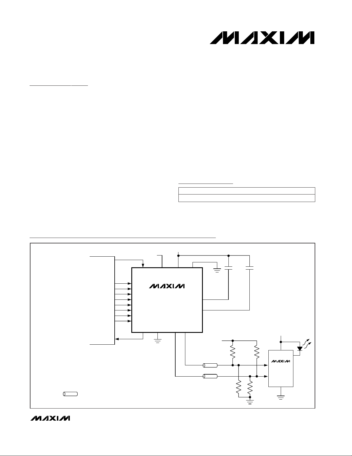
MAX3690
MAX3668
SD-
GND
PCLKO
38.88MHz TTL CRYSTAL
REFERENCE
PCLKI RCLK V
CC
CKSET
SD+
FIL-
FIL+
130Ω 130Ω
82Ω
82Ω
V
CC
= +3.3V
V
CC
= +3.3V
V
CC
= +3.3V
OVERHEAD
GENERATION
PD7
PD6
PD5
PD4
PD3
PD2
PD1
PD0
THIS SYMBOL REPRESENTS A TRANSMISSION LINE
OF CHARACTERISTIC IMPEDANCE (Z
0
= 50Ω).
1µF
1µF
Typical Operating Circuit
19-4774; Rev 1; 4/99
PART
MAX3690ECJ -40°C to +85°C
TEMP. RANGE PIN-PACKAGE
32 TQFP
Ordering Information
Pin Configuration appears at end of data sheet.
For free samples & the latest literature: http://www.maxim-ic.com, or phone 1-800-998-8800.
For small orders, phone 1-800-835-8769.

MAX3690
+3.3V, 622Mbps, SDH/SONET 8:1 Serializer
with Clock Synthesis and TTL Inputs
2 _______________________________________________________________________________________
ABSOLUTE MAXIMUM RATINGS
DC ELECTRICAL CHARACTERISTICS
(VCC= +3.0V to +3.6V, PECL loads = 50Ω ±1% to (VCC- 2V), TA= -40°C to +85°C, unless otherwise noted. Typical values are at
V
CC
= +3.3V, TA= +25°C.)
Stresses beyond those listed under “Absolute Maximum Ratings” may cause permanent damage to the device. These are stress ratings only, and functional
operation of the device at these or any other conditions beyond those indicated in the operational sections of the specifications is not implied. Exposure to
absolute maximum rating conditions for extended periods may affect device reliability.
Note 1: AC characteristics guaranteed by design and characterization.
Note 2: All TTL thresholds set to V
CC
/ 2.
Terminal Voltage (with respect to GND)
V
CC
.......................................................................-0.5V to +5V
All Inputs, FIL-, FIL+, PCLKO.................-0.5V to (V
CC
+ 0.5V)
Output Current
PECL Outputs (SD±).......................................................50mA
Continuous Power Dissipation (T
A
= +85°C)
TQFP (derate 10.2mW/°C above +85°C).....................663mW
Operating Temperature Range ...........................-40°C to +85°C
Storage Temperature Range.............................-60°C to +160°C
Lead Temperature (soldering, 10sec).............................+300°C
T
A
= 0°C to +85°C
PECL outputs unterminated
IOL= -400µA
IOH= 400µA
VIN= 0
VIN= V
CC
TA= 0°C to +85°C
CONDITIONS
VCC- 1.025 VCC- 0.88
mA60 100I
CC
Supply Current
V0.44V
OL
Output Low Voltage
V2.4V
OH
Output High Voltage
µA-10 10I
IL
Input Low Current
µA-10 10I
IH
Input High Current
VCC- 1.81 VCC- 1.62
V2.0V
IH
Input High Voltage
V0.8V
IL
Input Low Voltage
UNITSMIN TYP MAXSYMBOLPARAMETER
C
LOAD
= 15pF, V
OUT
= 0.8V to 2.0V
C
LOAD
= 15pF, V
OUT
= 0.8V to 2.0V
CONDITIONS
ps1000t
H
Parallel Data Hold Time
ps1200t
SU
MHz622.08f
SCLK
Serial Clock Rate
Parallel Data Setup Time
ns550t
F
TTL Output Fall Time
ns650t
R
TTL Output Rise Time
ns0 5.0t
SKEW
Allowable Parallel Clock Output
to Parallel Clock Input Delay
ps
RMS
11
Φ
0
Output Random Jitter
UNITSMIN TYP MAXSYMBOLPARAMETER
AC ELECTRICAL CHARACTERISTICS
(VCC= +3.0V to +3.6V, PECL loads = 50Ω ±1% to (VCC- 2V), all TTL thresholds set to VCC/2, TA= -40°C to +85°C, unless otherwise
noted. Typical values are at V
CC
= +3.3V, TA= +25°C.) (Note 1)
CKSET = 0 or V
CC
µA500I
CKSET
CKSET Input Current
TA= -40°C
V
VCC- 1.085 VCC- 0.88
V
OH
Output High Voltage
TA= -40°C
V
VCC- 1.83 VCC- 1.555
V
OL
Output Low Voltage
PECL OUTPUTS (SD±)
TTL INPUTS AND OUTPUTS (PCLKI, RCLK, PCLKO, PD_)
20% to 80% ps200t
R, tF
PECL Differential Output
Rise/Fall Time
MAX3690
+3.3V, 622Mbps, SDH/SONET 8:1 Serializer
with Clock Synthesis and TTL Inputs
_______________________________________________________________________________________
3
45
55
50
65
60
70
75
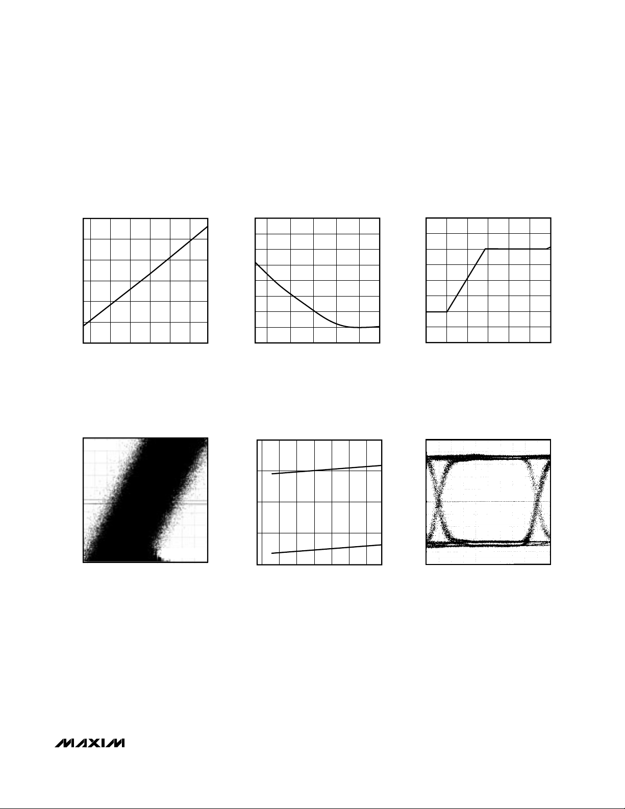
SUPPLY CURRENT vs. TEMPERATURE
MAX3690-01
TEMPERATURE (°C)
SUPPLY CURRENT (mA)
-50 25-25 0 50 75
100
-95
-80
-85
-90
-70
-75
-60
-65
-55
PARALLEL DATA SETUP TIME
vs. TEMPERATURE
MAX3690-02
TEMPERATURE (¡C)
PARALLEL DATA SETUP TIME (ps)
-40 25
-25
0507585
230
245
240
235
255
250
265
260
270
-40 25-25 0 50 75 85
PARALLEL DATA HOLD TIME
vs. TEMPERATURE
MAX3690-03
TEMPERATURE (°C)
PARALLEL DATA HOLD TIME (ps)
-5
0
5
10
15
00-50 50 100
ALLOWED PCLKO to PCLKI SKEW
vs. TEMPERATURE
MAX3690-07
TEMPERATURE (°C)
TIME (ns)
2mV/
div
5ps/div
SERIAL DATA RANDOM JITTER
(R
CLKI
= 77.76MHz)
MAX3690-05
TEMPERATURE (°C)
VCC = 3.3V
RJ = 4.66ps
RMS
__________________________________________Typical Operating Characteristics
(VCC= +3.3V, TA= +25°C, unless otherwise noted.)
100mV/
div
200ps/div
SERIAL-DATA OUTPUT EYE DIAGRAM
(622Mbps, PRBS)
MAX3690-08

MAX3690
+3.3V, 622Mbps, SDH/SONET 8:1 Serializer
with Clock Synthesis and TTL Inputs
4 _______________________________________________________________________________________
______________________________________________________________Pin Description
NAME FUNCTION
1–8 PD0–PD7 TTL Parallel-Data Inputs. Data is clocked in on the PCLKI signal’s positive transition.
9, 10, 17,
18, 19, 24,
25, 26,
31, 32
GND Ground
PIN
11 PCLKO
TTL Parallel-Clock Output. Use positive transition of PCLKO to clock the overhead management
circuit.
12, 13, 16,
21, 28, 29
V
CC
+3.3V Supply Voltage
20 CKSET
Reference Clock Rate Programming Pin.
CKSET = open: Reference clock rate = 77.76MHz
CKSET = 20kΩ to GND: Reference clock rate = 51.84MHz
CKSET = GND: Reference clock rate = 38.88MHz
15 SD+ Noninverting PECL Serial-Data Output
14 SD- Inverting PECL Serial-Data Output
30 PCLKI
TTL Parallel-Clock Input. Connect the incoming parallel-data-clock signal to the PCLKI input. The
active edge is the positive transitioning edge.
27 RCLK
TTL Reference-Clock Input. Connect a crystal reference clock (77.76MHz, 51.84MHz or 38.88MHz) to
the RCLK input. The active edge is the positive transitioning edge.
23 FIL+ Filter Capacitor Input. Connect a 1µF capacitor between FIL- and VCC.
_______________Detailed Description
The MAX3690 serializer comprises an 8-bit parallel
input register, an 8-bit shift register, control and timing
logic, a PECL output buffer, TTL input/output buffers,
and a frequency-synthesizing PLL (consisting of a
phase/frequency detector, loop filter/amplifier, voltagecontrolled oscillator, and programmable prescaler).
This device converts 8-bit-wide, 77Mbps parallel data
to 622Mbps serial data (Figure 1).
The PLL synthesizes an internal 622MHz reference
used to clock the output shift register. This clock is
generated by locking onto the external crystal reference clock signal (RCLK) operating at either
77.76MHz, 51.84MHz, or 38.88MHz. The incoming par-
allel data is clocked into the MAX3690 on the rising
transition of the parallel-clock-input signal (PCLKI). The
control and timing logic ensure proper operation if the
parallel-input register is latched within a window of time
that is defined with respect to the parallel-clock-output
signal (PCLKO). PCLKO is the synthesized 622MHz
internal serial-clock signal divided by eight. Parallelclock output to parallel-clock-input delay (skew) must
be observed. Figure 2 shows the timing diagram.
PECL Outputs
The serial-data PECL outputs (SD+, SD-) require 50Ω
DC termination to (VCC- 2V). See the
Alternative PECL-
Output Termination
section.
22 FIL- Filter Capacitor Input. Connect a 1µF capacitor between FIL- and VCC.

MAX3690
+3.3V, 622Mbps, SDH/SONET 8:1 Serializer
with Clock Synthesis and TTL Inputs
_______________________________________________________________________________________ 5
MAX3690
TTL
PD7
TTL
PD6
TTL
8-BIT
PARALLEL
INPUT
REGISTER
PHASE/FREQ
DETECT
CONTROL
8-BIT
SHIFT
REGISTER
PD5
TTL
PD4
TTL
PD3
TTL
PD2
TTL
PD1
TTL
TTL
PD0
TTL
PCLKI
CKSET
TTL
FIL+ FIL- PCLKO
VCO
RCLK
PECL
SDOH
SDOL
SHIFT
LATCH
PRE-
SCALER
Figure 1. Functional Diagram
t
SU
VALID PARALLEL DATA
PCLKO
PCLKI
PD_
SD
D7 D6 D5 D4 D3 D2
NOTE: PD7 = D7, PD6 = D6, PD5 = D5, PD4 = D4, PD3 = D3, PD2 = D2, PD1 = D1, PD0 = D0
D1 D0
t
H
t
SKEW
Figure 2. Timing Diagram

MAX3690
+3.3V, 622Mbps, SDH/SONET 8:1 Serializer
with Clock Synthesis and TTL Inputs
6 _______________________________________________________________________________________
__________Applications Information
Alternative PECL-Output Termination
Figure 3 shows alternative PECL-output-termination
methods. Use Thevenin-equivalent termination when a
(VCC- 2V) termination voltage is not available. If AC
coupling is necessary, be sure that the coupling
capacitor is placed following the 50Ω or Theveninequivalent DC termination.
Layout Techniques
For best performance, use good high-frequency layout
techniques. Filter voltage supplies and keep ground
connections short. Use multiple vias where possible.
Also, use controlled-impedance transmission lines to
interface with the MAX3690 data outputs.
MAX3690
SD+
SD-
V
CC
- 2V
50Ω 50Ω
Z
0
= 50Ω
HIGHIMPEDENCE
INPUTS
Z0 = 50Ω
MAX3690
SD+
SD-
+3.3V
130Ω
130Ω
82Ω 82Ω
Z0 = 50Ω
PECL
INPUTS
Z0 = 50Ω
Figure 3. Alternative PECL-Output Termination

MAX3690
+3.3V, 622Mbps, SDH/SONET 8:1 Serializer
with Clock Synthesis and TTL Inputs
_______________________________________________________________________________________ 7
TQFP
TOP VIEW
FIL+
FIL-
VCCCKSET
GND
GND
GND
GND
PD1
PD2
PD3
PD4
PD5
PD0
PD7
PD6
SD+
SD-
GND
V
CC
V
CC
PCLKO
V
CC
GND
GND
RCLK
GND
V
CC
V
CC
PCLKI
GND
GND
32
31
30
29
28
27
26
25
17
18
19
20
21
22
23
24
9
10
11
12
13
14
15
16
8
7
6
5
4
3
2
1
MAX3690
Pin Configuration

Maxim cannot assume responsibility for use of any circuitry other than circuitry entirely embodied in a Maxim product. No circuit patent licenses are
implied. Maxim reserves the right to change the circuitry and specifications without notice at any time.
8
_____________________Maxim Integrated Products, 120 San Gabriel Drive, Sunnyvale, CA 94086 408-737-7600
© 1999 Maxim Integrated Products Printed USA is a registered trademark of Maxim Integrated Products.
MAX3690
+3.3V, 622Mbps, SDH/SONET 8:1 Serializer
with Clock Synthesis and TTL Inputs
TQFPPO.EPS
Package Information
 Loading...