

Page 1
_________________General Description
The MAX3681 deserializer is ideal for converting
622Mbps serial data to 4-bit-wide, 155Mbps parallel
data in ATM and SDH/SONET applications. Operating
from a single +3.3V supply, this device accepts PECL
serial clock and data inputs, and delivers low-voltage
differential-signal (LVDS) clock and data outputs for
interfacing with high-speed digital circuitry. It also provides an LVDS synchronization input that enables data
realignment and reframing.
The MAX3681 is available in the extended-industrial
temperature range (-40°C to +85°C), in a 24-pin SSOP
package.
__________________________Applications
622Mbps SDH/SONET Transmission Systems
622Mbps ATM/SONET Access Nodes
Add/Drop Multiplexers
Digital Cross Connects
______________________________Features
♦ Single +3.3V Supply
♦ 622Mbps Serial to 155Mbps Parallel Conversion
♦ 265mW Power
♦ LVDS Data Outputs and Synchronization Inputs
♦ Synchronization Input for Data Realignment and
Reframing
♦ Differential 3.3V PECL Clock and Data Inputs
MAX3681
+3.3V, 622Mbps, SDH/SONET
1:4 Deserializer with LVDS Outputs
________________________________________________________________ Maxim Integrated Products 1
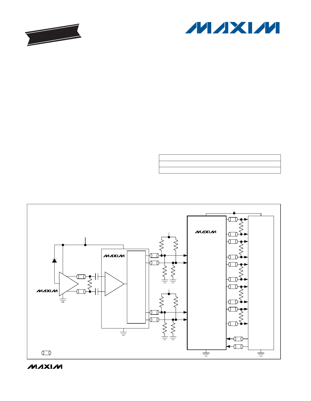
MAX3675
MAX3664
MAX3681
DATA
AND
CLOCK
RECOVERY
OVERHEAD
TERMINATION
LIMITING
AMP
PREAMP
100Ω
100Ω*
100Ω*
100Ω*
100Ω*
100Ω*
PHOTODIODE
VCC = +3.3V
V
CC
= +3.3V
PD3+
PD3-
PD2+
PD2-
PD1+
PD1-
PD0+
PD0-
PCLK+
PCLK-
SYNC+
SYNC-
SD+
SD-
*REQUIRED ONLY IF OVERHEAD CIRCUIT DOES NOT INCLUDE INTERNAL INPUT TERMINATION.
THIS SYMBOL REPRESENTS A TRANSMISSION LINE OF CHARACTERISTIC IMPEDANCE Z0 = 50Ω.
V
CC
GND
130Ω 130Ω
82Ω 82Ω
VCC = +3.3V
130Ω 130Ω
82Ω 82Ω
VCC = +3.3V
SCLK+
SCLK-
___________________________________________________________________Typical Operating Circuit
19-1091; Rev 1; 5/04
PART
MAX3681EAG -40°C to +85°C
TEMP RANGE PIN-PACKAGE
24 SSOP
EVALUATION KIT
AVAILABLE
________________Ordering Information
+Denotes Lead Free Package
For pricing, delivery, and ordering information, please contact Maxim/Dallas Direct! at
1-888-629-4642, or visit Maxim’s website at www.maxim-ic.com.
MAX3681EAG+ -40°C to +85°C 24 SSOP
Pin Configuration appears at end of data sheet.
Page 2
MAX3681
+3.3V, 622Mbps, SDH/SONET
1:4 Deserializer with LVDS Outputs
2 _______________________________________________________________________________________
ABSOLUTE MAXIMUM RATINGS
DC ELECTRICAL CHARACTERISTICS
(VCC= +3.0V to +3.6V, differential loads = 100Ω, TA= -40°C to +85°C, unless otherwise noted. Typical values are at VCC= +3.3V,
T
A
= +25°C.)
Stresses beyond those listed under “Absolute Maximum Ratings” may cause permanent damage to the device. These are stress ratings only, and functional
operation of the device at these or any other conditions beyond those indicated in the operational sections of the specifications is not implied. Exposure to
absolute maximum rating conditions for extended periods may affect device reliability.
Note 1: AC Characteristics guaranteed by design and characterization.
Terminal Voltage (with respect to GND)
V
CC
...........................................................................-0.5V to 5V
PECL Inputs (SD+/-, SCLK+/-).................................V
CC
+ 0.5V
LVDS Inputs (SYNC+/-)............................................V
CC
+ 0.5V
Output Current, LVDS Outputs (PCLK+/-, PD_+/-) .............10mA
Continuous Power Dissipation (T
A
= +85°C)
SSOP (derate 8.00mW/°C above +85°C) ......................520mW
Operating Temperature Range ...........................-40°C to +85°C
Storage Temperature Range .............................-65°C to +160°C
Lead Temperature (soldering, 10sec) .............................+300°C
TA= +25°C
Common-mode voltage = 50mV
Differential input voltage = 100mV
VIN= V
IH(MAX)
VIN= V
IL(MAX)
CONDITIONS
%±1 ±10ΔR
O
Change in Magnitude of SingleEnded Output Resistance for
Complementary States
Ω40 70 140R
O
Single-Ended Output Resistance
mV25ΔV
OS
Change in Magnitude of Output
Offset Voltage for Complementary
States
V1.125 1.275V
OS
Output Offset Voltage
mV25ΔV
OD
Change in Magnitude of Differential
Output Voltage for Complementary
States
mV250 400V
OD
Differential Output Voltage
V0.925V
OL
Output Low Voltage
V1.475V
OH
Output High Voltage
VVCC- 1.16 VCC- 0.88V
IH
Input High Voltage
mA55 80 120I
CC
Supply Current
Ω85 100 115R
IN
Differential Input Resistance
mV70V
HYST
Threshold Hysteresis
mV-100 100V
IDTH
Differential Input Threshold
V0 2.4V
I
Input Voltage Range
VVCC- 1.81 VCC- 1.48V
IL
Input Low Voltage
µA-10 10I
IH
Input High Current
µA-10 10I
IL
Input Low Current
UNITSMIN TYP MAXSYMBOLPARAMETER
CONDITIONS
ps50t
H
Serial Data Hold Time
ps800t
SU
MHz622f
SCLK
Maximum Serial Clock Frequency
Serial Data Setup Time
ps200 550 900t
CLK-Q
Parallel Clock to Data Output Delay
UNITSMIN TYP MAXSYMBOLPARAMETER
PECL INPUTS (SD+/-, SCLK+/-)
LVDS INPUTS AND OUTPUTS (SYNC+/-, PCLK+/-, PD_+/-)
AC ELECTRICAL CHARACTERISTICS
(VCC= +3.0V to +3.6V, differential loads = 100Ω, TA= +25°C, unless otherwise noted.) (Note 1)
Page 3
MAX3681
+3.3V, 622Mbps, SDH/SONET
1:4 Deserializer with LVDS Outputs
_______________________________________________________________________________________ 3
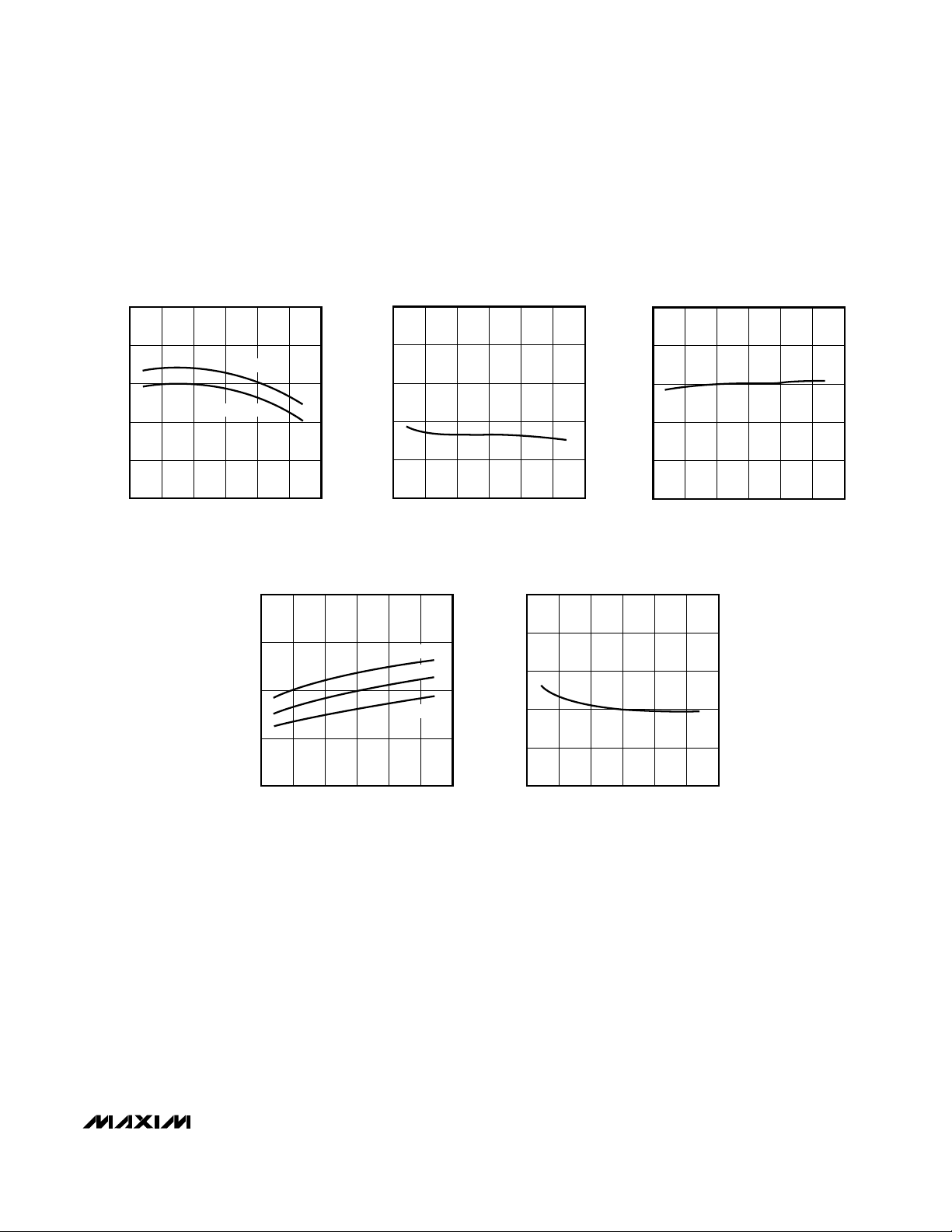
1.8
0
MAXIMUM SERIAL CLOCK FREQUENCY
vs. TEMPERATURE
MAX3681-01
MAX SERIAL CLOCK FREQUENCY (GHz)
-25
1.6
25 50
1.4
1.2
1.0
75
100
TEMPERATURE (°C)
2.0
-50
VCC = 3.0V
VCC = 3.6V
0
SUPPLY CURRENT
vs. TEMPERATURE
MAX3681-02
SUPPLY CURRENT (mA)
-25
100
25 50
80
60
40
75
100
TEMPERATURE (°C)
120
-50
VCC = +3.0V
VCC = +3.6V
VCC = +3.3V
360
0
SERIAL DATA-SETUP TIME
vs. TEMPERATURE
MAX3681-03
SERIAL DATA-SETUP TIME (ps)
-25
320
25 50
280
240
200
75
100
TEMPERATURE (°C)
400
-50
-140
0
SERIAL DATA-HOLD TIME
vs. TEMPERATURE
MAX3681-04
SERIAL DATA-HOLD TIME (ps)
-25
-180
25 50
-220
-260
-300
75
100
TEMPERATURE (°C)
-100
-50
650
0
PARALLEL CLOCK TO DATA
OUTPUT PROPAGATION DELAY
vs. TEMPERATURE
MAX3681-05
PARALLEL CLOCK TO DATA
PROPAGATION DELAY (ps)
-25
600
25 50
550
500
450
75
100
TEMPERATURE (°C)
700
-50
__________________________________________Typical Operating Characteristics
(VCC= +3.0V to +3.6V, differential loads = 100Ω, unless otherwise noted.)
Page 4
MAX3681
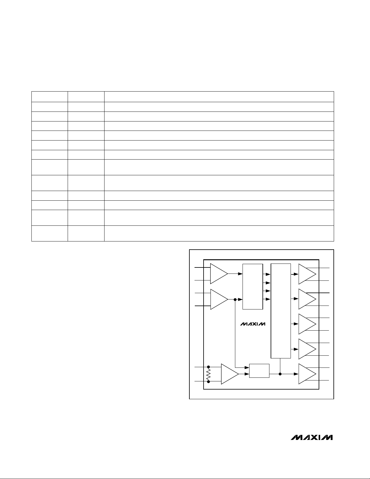
_______________Detailed Description
The MAX3681 deserializer uses a 4-bit shift register,
4-bit parallel output register, 2-bit counter, PECL input
buffers, and low-voltage differential-signal (LVDS)
input/output buffers to convert 622Mbps serial data to
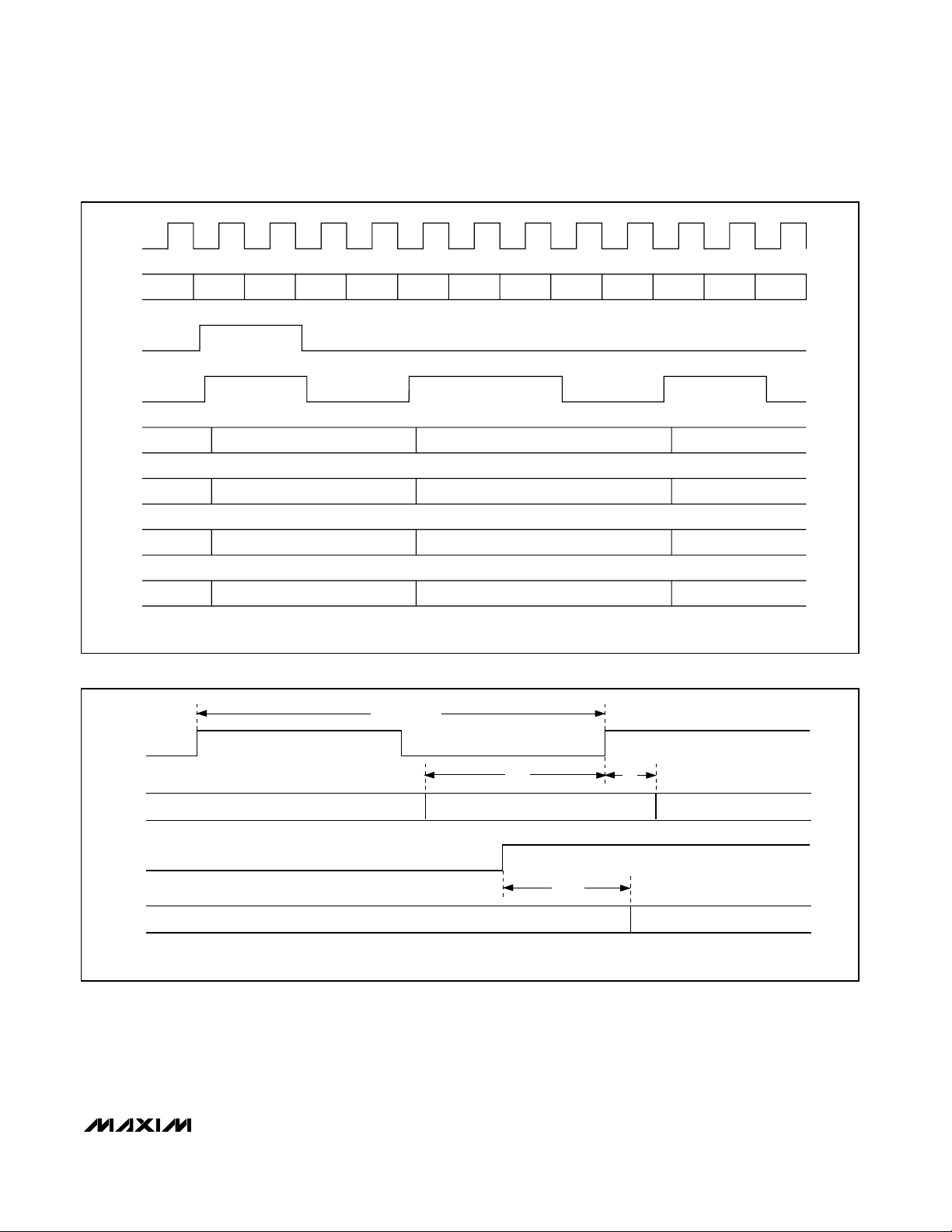
4-bit-wide, 155Mbps parallel data (Figure 1).
The input shift register continuously clocks incoming
data on the positive transition of the serial clock (SCLK)
input signal. The 2-bit counter generates a parallel output clock (PCLK) by dividing down the serial clock frequency. The PCLK signal is used to clock the parallel
output register. During normal operation, the counter
divides the SCLK frequency by four, causing the output
register to latch every four bits of incoming serial data.
The synchronization inputs (SYNC+, SYNC-) are used
for data realignment and reframing. When the SYNC
signal is pulsed high for at least two SCLK cycles, the
parallel output data is delayed by one SCLK cycle. This
realignment is guaranteed to occur within two PCLK
cycles of the SYNC signal’s positive transition. As a
result, the first incoming bit of data during that PCLK
cycle is dropped, shifting the alignment between PCLK
and data by one bit.
See Figure 2 for the functional timing diagram and
Figure 3 for the timing parameters diagram.
+3.3V, 622Mbps, SDH/SONET
1:4 Deserializer with LVDS Outputs
4 _______________________________________________________________________________________
______________________________________________________________Pin Description
NAME FUNCTION
1, 2, 5, 8, 12 V
CC
+3.3V Supply Voltage
3 SD+ Noninverting PECL Serial Data Input. Data is clocked on the SCLK signal’s positive transition.
PIN
4 SD- Inverting PECL Serial Data Input. Data is clocked on the SCLK signal’s positive transition.
6 SCLK+ Noninverting PECL Serial Clock Input
11 SYNC-
Inverting LVDS Synchronizing Pulse Input. Pulse the SYNC signal high for at least two SCLK
periods to shift the data alignment by dropping one bit.
10 SYNC+
Noninverting LVDS Synchronizing Pulse Input. Pulse the SYNC signal high for at least two SCLK
periods to shift the data alignment by dropping one bit.
9, 15, 22 GND Ground
7 SCLK- Inverting PECL Serial Clock Input
17, 19, 21, 24 PD0+ to PD3+
Noninverting LVDS Parallel Data Outputs. Data is updated on the positive transition of the PCLK signal.
See Figure 2 for the relationship between serial-data-bit position and output-data-bit assignment.
16, 18, 20, 23 PD0- to PD3-
Inverting LVDS Parallel Data Outputs. Data is updated on the positive transition of the PCLK signal.
See Figure 2 for the relationship between serial-data-bit position and output-data-bit assignment.
14 PCLK+ Noninverting LVDS Parallel Clock Output
13 PCLK- Inverting LVDS Parallel Clock Output
Figure 1. Functional Diagram
SD+
PECL
SD-
SCLK+
SCLK-
SYNC+
SYNC-
PECL
100Ω
MAX3681
LVDS
4-BIT
SHIFT
REGISTER
2-BIT
COUNTER
4-BIT
PARALLEL
OUTPUT
REGISTER
LVDS
LVDS
LVDS
LVDS
LVDS
PD3+
PD3-
PD2+
PD2-
PD1+
PD1-
PD0+
PD0-
PCLK+
PCLK-
Page 5
MAX3681
+3.3V, 622Mbps, SDH/SONET
1:4 Deserializer with LVDS Outputs
_______________________________________________________________________________________ 5
SCLK
SD
SYNC
PCLK
PD3
PD2
PD1
PD0
D1- D0 D1
D4- D0 D5
D3- D1 D6
D2- D2 D7
D1- D3 D8
D2 D3 D4 D5 D6 D7 D8 D9 D10 D11
NOTE: SIGNALS SHOWN ARE DIFFERENTIAL. FOR EXAMPLE, SCLK = (SCLK+) - (SCLK-).
Figure 2. Functional Timing Diagram
SCLK
SD
PCLK
PD0–PD3
NOTE: SIGNALS SHOWN ARE DIFFERENTIAL. FOR EXAMPLE, SCLK = (SCLK+) - (SCLK-).
t
SCLK
= 1 / f
SCLK
t
SU
t
CLK-Q
t
H
Figure 3. Timing Parameters
Page 6

MAX3681
Low-Voltage Differential-Signal (LVDS)
Inputs and Outputs
The MAX3681 features LVDS inputs and outputs for
interfacing with high-speed digital circuitry. The LVDS
standard is based on the IEEE 1596.3 LVDS specification. This technology uses 250mVp-p to 400mVp-p, differential low-voltage swings to achieve fast transition
times, minimized power dissipation, and noise immunity.
The parallel clock and data LVDS outputs (PCLK+,
PCLK-, PD_+, PD_-) require 100Ω differential DC termi-
nation between the inverting and noninverting outputs
for proper operation. Do not terminate these outputs to
ground.
The synchronization LVDS inputs (SYNC+, SYNC-) are
internally terminated with 100Ω of differential input
resistance, and therefore do not require external termination.
PECL Inputs
The serial data and clock PECL inputs (SD+, SD-,
SCLK+, SCLK-) require 50Ω termination to (VCC- 2V)
when interfacing with a PECL source (see the
Alternative PECL Input Termination section).
__________Applications Information
Alternative PECL Input Termination
Figure 4 shows alternative PECL input-termination
methods. Use Thevenin-equivalent termination when a
(VCC- 2V) termination voltage is not available. If AC
coupling is necessary, such as when interfacing with
an ECL-output device, use the ECL AC-coupling termination.
Layout Techniques
For best performance, use good high-frequency layout
techniques. Filter voltage supplies and keep ground
connections short. Use multiple vias where possible.
Also, use controlled impedance transmission lines to
interface with the MAX3681 data inputs and outputs.
+3.3V, 622Mbps, SDH/SONET
1:4 Deserializer with LVDS Outputs
6 _______________________________________________________________________________________
MAX3681
PECL
INPUTS
Z
O
= 50Ω
ZO = 50Ω
130Ω
82Ω
130Ω
82Ω
+3.3V
MAX3681
PECL
INPUTS
ZO = 50Ω
50Ω
Z
O
= 50Ω
1.6k
2.7k
1.6k
2.7k
+3.3V
-2V
50Ω
-2V
THEVENIN-EQUIVALENT TERMINATION
ECL AC-COUPLING TERMINATION
Figure 4. Alternative PECL Input Termination
Page 7

MAX3681
+3.3V, 622Mbps, SDH/SONET
1:4 Deserializer with LVDS Outputs
_______________________________________________________________________________________ 7
___________________Chip Information
TRANSISTOR COUNT: 724
24
23
22
21
20
19
18
17
1
2
3
4
5
6
7
8
PD3+
PD3-
GND
PD2+
PD2-
PD1+
PD1-
PD0+
PD0-
GND
PCLK+
PCLK-
V
CC
V
CC
SD+
SD-
V
CC
SCLK+
SCLK-
V
CC
GND
SYNC+
SYNC-
V
CC
TOP VIEW
16
15
14
13
9
10
11
12
SSOP
MAX3681
__________________Pin Configuration
Page 8
Maxim cannot assume responsibility for use of any circuitry other than circuitry entirely embodied in a Maxim product. No circuit patent licenses are
implied. Maxim reserves the right to change the circuitry and specifications without notice at any time.
8 ___________________Maxim Integrated Products, 120 San Gabriel Drive, Sunnyvale, CA 94086 (408) 737-7600
© 1996 Maxim Integrated Products Printed USA is a registered trademark of Maxim Integrated Products.
MAX3681
+3.3V, 622Mbps, SDH/SONET
1:4 Deserializer with LVDS Outputs
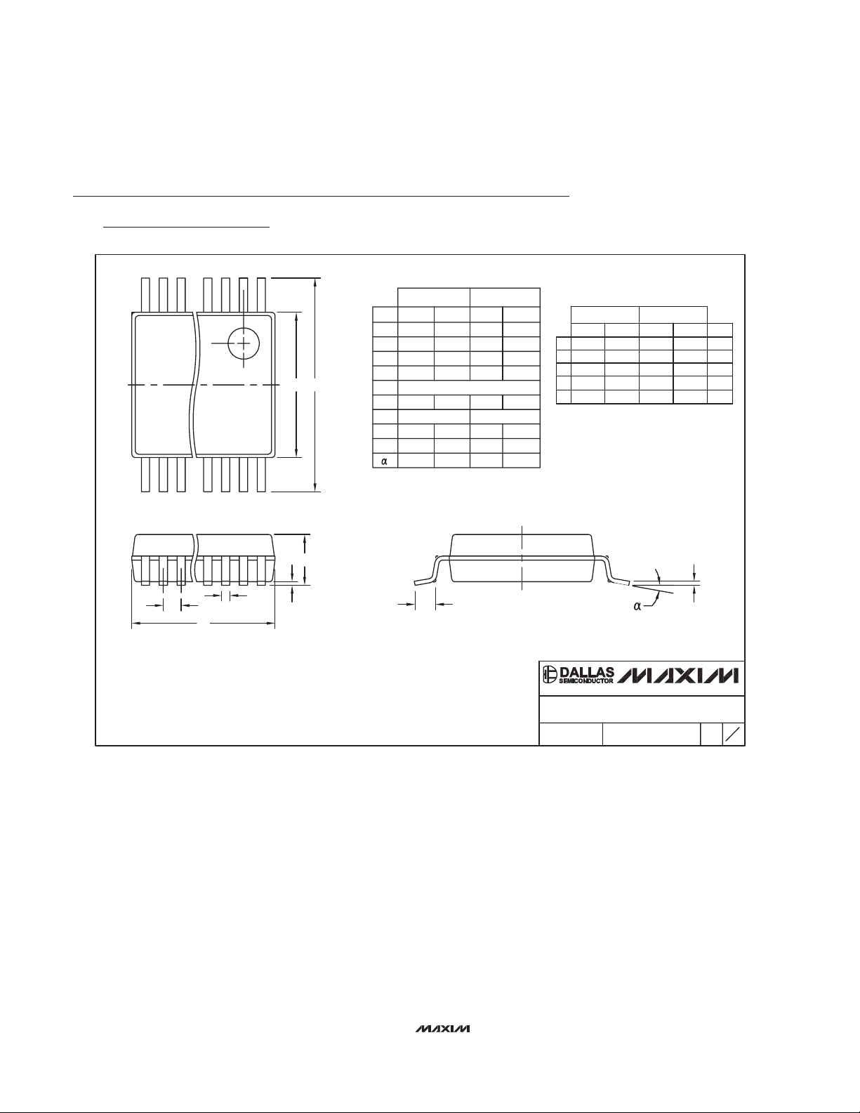
SSOP.EPS
PACKAGE OUTLINE, SSOP, 5.3 MM
1
1
21-0056
C
REV.DOCUMENT CONTROL NO.APPROVAL
PROPRIETARY INFORMATION
TITLE:
NOTES:
1. D&E DO NOT INCLUDE MOLD FLASH.
2. MOLD FLASH OR PROTRUSIONS NOT TO EXCEED .15 MM (.006").
3. CONTROLLING DIMENSION: MILLIMETERS.
4. MEETS JEDEC MO150.
5. LEADS TO BE COPLANAR WITHIN 0.10 MM.
7.90
H
L
0∞
0.301
0.025
8∞
0.311
0.037
0∞
7.65
0.63
8∞
0.95
MAX
5.38
MILLIMETERS
B
C
D
E
e
A1
DIM
A
SEE VARIATIONS
0.0256 BSC
0.010
0.004
0.205
0.002
0.015
0.008
0.212
0.008
INCHES
MIN
MAX
0.078
0.65 BSC
0.25
0.09
5.20
0.05
0.38
0.20
0.21
MIN
1.73 1.99
MILLIMETERS
6.07
6.07
10.07
8.07
7.07
INCHES
D
D
D
D
D
0.239
0.239
0.397
0.317
0.278
MIN
0.249
0.249
0.407
0.328
0.289
MAX
MIN
6.33
6.33
10.33
8.33
7.33
14L
16L
28L
24L
20L
MAX
N
A
D
e
A1
L
C
HE
N
12
B
0.068
Package Information
(The package drawing(s) in this data sheet may not reflect the most current specifications. For the latest package outline information
go to www.maxim-ic.com/packages
.)
 Loading...