

Page 1
_________________General Description
The MAX3680/MAX3680A deserializer is ideal for converting 622Mbps serial data to 8-bit-wide, 77Mbps parallel data in ATM and SDH/SONET applications.
Operating from a single +3.3V supply, this device
accepts PECL serial clock and data inputs, and delivers TTL clock and data outputs. The MAX3680 also provides a TTL synchronization input that enables data
realignment and reframing.
The MAX3680/MAX3680A is available in the extendedindustrial temperature range (-40°C to +85°C), in a 28pin SSOP package.
__________________________Applications
622Mbps SDH/SONET Transmission Systems
622Mbps ATM/SONET Access Nodes
Add/Drop Multiplexers
Digital Cross-Connects
______________________________Features
♦♦
Single +3.3V Supply
♦♦
622Mbps Serial to 77Mbps Parallel Conversion
♦♦
165mW Power
♦♦
Synchronization Input for Data Realignment and
Reframing (MAX3680)
♦♦
Differential 3.3V PECL Clock and Data Inputs
♦♦
TTL Data Outputs
MAX3680/MAX3680A
+3.3V, 622Mbps, SDH/SONET
1:8 Deserializer with TTL Outputs
________________________________________________________________
Maxim Integrated Products
1
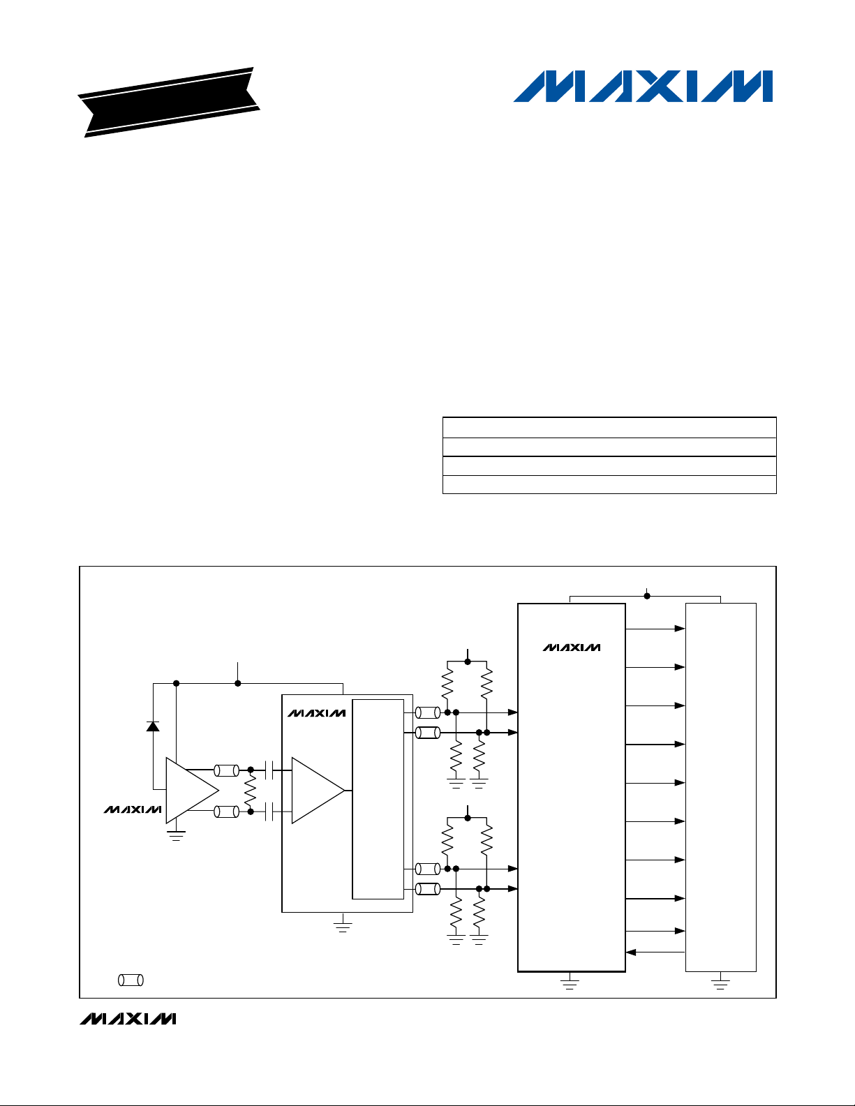
___________________________________________________________________Typical Operating Circuit
19-1210; Rev 3; 3/07
________________Ordering Information
Pin Configuration appears at end of data sheet.
EVALUATION KIT
AVAILABLE
For pricing, delivery, and ordering information, please contact Maxim/Dallas Direct! at
1-888-629-4642, or visit Maxim’s website at www.maxim-ic.com.
+
Denotes lead-free package.
PART TEMP RANGE PIN-PACKAGE
MAX3680EAI -40°C to +85° C 28 SSOP
MAX3680EAI+ -40°C to +85°C 28 SSOP
MAX3680AEAI -40°C to +85°C 28 SSOP
= +3.3V
V
CC
VCC = +3.3V
PHOTODIODE
PREAMP
MAX3664
THIS SYMBOL REPRESENTS A TRANSMISSION LINE OF CHARACTERISTIC IMPEDANCE Z0 = 50Ω.
100Ω
MAX3675
LIMITING
AMP
DATA
AND
CLOCK
RECOVERY
VCC = +3.3V
130Ω 130Ω
82Ω 82Ω
VCC = +3.3V
130Ω 130Ω
82Ω 82Ω
SD+
SD-
SCLK+
SCLK-
V
CC
MAX3680/
MAX3680A
GND
PD7
PD6
PD5
PD4
PD3
PD2
PD1
PD0
PCLK
SYNC
OVERHEAD
TERMINATION
Page 2
MAX3680/MAX3680A
+3.3V, 622Mbps, SDH/SONET
1:8 Deserializer with TTL Outputs
2 _______________________________________________________________________________________
ABSOLUTE MAXIMUM RATINGS
DC ELECTRICAL CHARACTERISTICS
(VCC= +3.0V to +3.6V, TA= -40°C to +85°C, unless otherwise noted. Typical values are at VCC= +3.3V, TA= +25°C.)
Stresses beyond those listed under “Absolute Maximum Ratings” may cause permanent damage to the device. These are stress ratings only, and functional
operation of the device at these or any other conditions beyond those indicated in the operational sections of the specifications is not implied. Exposure to
absolute maximum rating conditions for extended periods may affect device reliability.
Note 2: AC characteristics guaranteed by design and characterization.
Note 1: The SYNC input is available only on the MAX3680.
Terminal Voltage (with respect to GND)
V
CC
........................................................................-0.5V to +5V
PECL Inputs (SD+/-, SCLK+/-) ................-0.5V to (V
CC
+ 0.5V)
TTL Input (SYNC) ....................................-0.5V to (V
CC
+ 0.5V)
TTL Outputs (PCLK, PD_)........................-0.5V to (V
CC
+ 0.5V)
Continuous Power Dissipation (T
A
= +85°C)
SSOP (derate 9.52mW/°C above +85°C) .....................619mW
Operating Temperature Range ...........................-40°C to +85°C
Storage Temperature Range .............................-65°C to +160°C
Lead Temperature (soldering, 10s) .................................+300°C
TTL outputs = high
VIN= V
IL(MAX)
VIN= V
IH(MAX)
VIN= V
IH(MAX)
VIN= V
IL(MAX)
Output sinking = 400µA
Output sourcing = 400µA
CONDITIONS
V0 0.44V
OL
Output Low Voltage
V2.4 V
CC
V
OH
Output High Voltage
VVCC- 1.16 VCC- 0.88V
IH
Input High Voltage
mA25 50 90I
CC
Supply Current
µA-10 10I
IL
Input Low Current
µA-10 10I
IH
Input High Current
V0.8V
IL
Input Low Voltage
V2.0V
IH
Input High Voltage
VVCC- 1.81 VCC- 1.48V
IL
Input Low Voltage
µA-10 10I
IH
Input High Current
µA-10 10I
IL
Input Low Current
UNITSMIN TYP MAXSYMBOLPARAMETER
CONDITIONS
ps50t
H
Serial Data Hold Time
ps800t
SU
MHz622f
SCLK
Maximum Serial Clock Frequency
Serial Data Setup Time
UNITSMIN TYP MAXSYMBOLPARAMETER
PECL INPUTS (SD+/-, SCLK+/-)
TTL INPUT AND OUTPUTS (SYNC, PCLK, PD_) (Note 1)
AC ELECTRICAL CHARACTERISTICS
(VCC= +3.0V to +3.6V, TA= +25°C, unless otherwise noted.) (Note 2)
VCC= +3.3V, CL= 18pF ps-200 500 2000t
CLK-Q
Parallel Clock to Data Output Delay
Page 3
MAX3680/MAX3680A
+3.3V, 622Mbps, SDH/SONET
1:8 Deserializer with TTL Outputs
_______________________________________________________________________________________
3
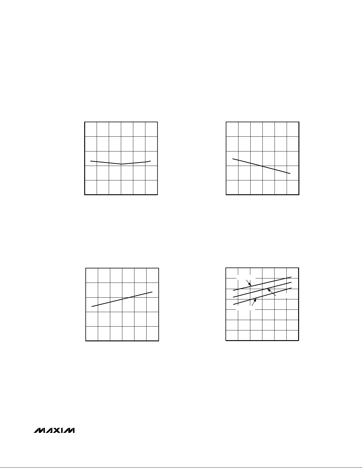
__________________________________________Typical Operating Characteristics
(VCC= +3.0V to +3.6V, unless otherwise noted.)
MAXIMUM SERIAL-CLOCK FREQUENCY
1.3
1.2
1.1
1.0
0.9
SERIAL CLOCK FREQUENCY (GHz)
0.8
-50
vs. TEMPERATURE
0
-25
TEMPERATURE (°C)
25 50
400
MAX3680-01
360
320
280
SERIAL DATA-SETUP TIME (ps)
240
100
75
200
SERIAL DATA SETUP TIME
vs. TEMPERATURE
0
-25
-50
TEMPERATURE (°C)
25 50
MAX3680-02
100
75
SERIAL DATA HOLD TIME
vs. TEMPERATURE
-100
-160
-220
-280
SERIAL DATA-HOLD TIME (ps)
-340
-400
-50
-25
TEMPERATURE (°C)
0
25 50
SUPPLY CURRENT
vs. TEMPERATURE
70
MAX3680-03
100
75
60
50
40
30
20
SUPPLY CURRENT (mA)
10
0
-50
VCC = +3.6V
VCC = +3.0V
-25
TEMPERATURE (°C)
VCC = +3.3V
25 50
0
MAX3680-04
100
75
Page 4

MAX3680/MAX3680A
Detailed Description
The MAX3680/MAX3680A deserializer uses an 8-bit
shift register, 8-bit parallel output register, 3-bit counter,
PECL input buffers, and TTL input/output buffers to
convert 622Mbps serial data to 8-bit-wide, 77Mbps parallel data (Figure 1).
The input shift register continuously clocks incoming
data on the positive transition of the serial clock (SCLK)
input signal. The 3-bit counter generates a parallel output
clock (PCLK) by dividing down the serial clock frequency. The PCLK signal is used to clock the parallel output
register. During normal operation, the counter divides the
SCLK frequency by eight, causing the output register to
latch every eight bits of incoming serial data.
The MAX3680 synchronization input (SYNC) is used for
data realignment and reframing. When the SYNC signal
is pulsed high for at least two SCLK cycles, PCLK is
delayed by one SCLK cycle, causing the first incoming
bit of the serial input data stream to be dropped. This
realignment is guaranteed to occur within two PCLK
cycles of the SYNC rising edge.
See Figure 2 for the functional timing diagrams and
Figure 3 for the timing parameters diagram.
+3.3V, 622Mbps, SDH/SONET
1:8 Deserializer with TTL Outputs
4 _______________________________________________________________________________________
Pin Description
Figure 1. Functional Diagram
PIN
MAX3680 MAX3680A
1, 2, 5, 8,
14, 18, 25
1, 2, 5, 8,
14, 18, 25
NAME FUNCTION
V
+3.3V Supply Voltage
CC
3 3
4 4
6 6
7 7
9, 11, 12,
16, 20, 23,
27
11, 12, 16,
20, 23, 27
10 —
— 9, 10
13 13
15, 17, 19,
21, 22, 24,
26, 28
15, 17, 19,
21, 22, 24,
26, 28
SD+
SD- Inverting PECL Serial Data Input. Data is clocked on the SCLK signal’s positive transition.
SCLK+ Noninverting PECL Serial Clock Input
SCLK- Inverting PECL Serial Clock Input
GND Ground
SYNC
N.C. No Connection
PCLK TTL Parallel Clock Output
PD0–PD7
Noninverting PECL Serial Data Input. Data is clocked on the SCLK signal’s positive
transition.
TTL Synchronization Pulse Input. Pulse high for at least two SCLK periods to shift the data
alignment by dropping one bit in the serial input data stream.
TTL Parallel Data Outputs. Data is updated on the falling edge of PCLK. See Figure 2 for the
relationship between serial-data-bit position and output-data-bit assignment.
SD+
PECL
SD-
SCLK+
SCLK-
SYNC
PECL
TTL
REGISTER
MAX3680/
MAX3680A
8-BIT
SHIFT
COUNTER
3-BIT
8-BIT
PARALLEL
OUTPUT
REGISTER
TTL
TTL
TTL
TTL
TTL
TTL
TTL
TTL
TTL
PD7
PD6
PD5
PD4
PD3
PD2
PD1
PD0
PCLK
Page 5

MAX3680/MAX3680A
+3.3V, 622Mbps, SDH/SONET
1:8 Deserializer with TTL Outputs
_______________________________________________________________________________________ 5
SCLK*
Figure 2a. Functional Timing Diagram—Normal Operation
D1- D0 D1
SD*
PCLK
PD7
PD6
PD5
PD4
PD3
PD2
PD1
PD0
* SIGNAL SHOWN IS DIFFERENTIAL. FOR EXAMPLE, SCLK = (SCLK+) - (SCLK-).
D2 D3 D4 D5 D6 D7 D9 D10 D11 D12 D13 D14 D15 D16 D17 D18D8
D8-
D7-
D6-
D5-
D4-
D3-
D2-
D1-
D0
D1 D9
D2 D10
D3 D11
D4 D12
D5 D13
D6 D14
D7 D15
D8
Page 6

MAX3680/MAX3680A
+3.3V, 622Mbps, SDH/SONET
1:8 Deserializer with TTL Outputs
6 _______________________________________________________________________________________
Figure 2b. Functional Timing Diagram—SYNC Operation (MAX3680)
Figure 3. Timing Parameters
SCLK*
D1- D0 D1
SD*
SYNC
PCLK
PD7
PD6
PD5
PD4
PD3
PD2
PD1
PD0
* SIGNAL SHOWN IS DIFFERENTIAL. FOR EXAMPLE, SCLK = (SCLK+) - (SCLK-).
D2 D3 D4 D5 D6 D7 D9 D10 D11 D12 D13 D14 D15 D16 D17 D18D8
D8- D1 D9
D7- D2 D10
D6- D3 D11
D5- D4 D12
D4- D5 D13
D3- D6 D14
D2- D7 D15
D1- D8 D16
t
= 1 / f
SCLK
SCLK
SCLK*
SD*
PCLK
PD0–PD7
* SIGNAL SHOWN IS DIFFERENTIAL. FOR EXAMPLE, SCLK = (SCLK+) - (SCLK-).
t
SU
t
CLK-Q
t
H
Page 7

MAX3680/MAX3680A
+3.3V, 622Mbps, SDH/SONET
1:8 Deserializer with TTL Outputs
_______________________________________________________________________________________ 7
PECL Inputs
The serial data and clock PECL inputs (SD+, SD-,
SCLK+, SCLK-) require 50Ω termination to (VCC- 2V)
when interfacing with a PECL source (see
Alternative
PECL Input Termination
).
Applications Information
Alternative PECL Input Termination
Figure 4 shows alternative PECL input-termination
methods. Use Thevenin-equivalent termination when a
(VCC- 2V) termination voltage is not available. If AC
coupling is necessary, such as when interfacing with
an ECL-output device, use the ECL AC-coupling termination.
Layout Techniques
For best performance, use good high-frequency layout
techniques. Filter voltage supplies and keep ground
connections short. Use multiple vias where possible.
Also, use controlled impedance transmission lines to
interface with the MAX3680 data inputs.
Figure 4. Alternative PECL Input Termination
28
27
26
25
24
23
22
21
20
19
18
17
16
15
1
2
3
4
5
6
7
8
9
10
11
12
13
14
PD7
GND
PD6
V
CC
PD5
GND
PD0
PD4
PD3
GND
PD2
V
CC
PD1
GND
V
CC
() MAX3680A ONLY.
PCLK
GND
GND
SYNC
(N.C.)
GND
(N.C.)
V
CC
SCLK-
SCLK+
V
CC
SD-
SD+
V
CC
V
CC
SSOP
TOP VIEW
MAX3680/
MAX3680A
Pin Configuration
Chip Information
TRANSISTOR COUNT: 1346
+3.3V
+3.3V
ZO = 50Ω
Z
= 50Ω
O
THEVENIN-EQUIVALENT TERMINATION
82Ω
2.7k
130Ω
82Ω
1.6k
2.7k
130Ω
= 50Ω
Z
O
ZO = 50Ω
ECL AC-COUPLING TERMINATION
1.6k
50Ω
-2V
50Ω
-2V
MAX3680/
MAX3680A
PECL
INPUTS
MAX3680/
MAX3680A
PECL
INPUTS
Page 8

________________________________________________________Package Information
MAX3680/MAX3680A
+3.3V, 622Mbps, SDH/SONET
1:8 Deserializer with TTL Outputs
Revision History
Rev 0; 3/97: Initial MAX3680 release.
Rev 1; 11/00: Changed t
CLK-Q
max from 1300ps to 2000ps (page 2); replaced TOC3 (page 3).
Rev 2; 7/04: Added lead-free package to Ordering Information table (page 1).
Rev 3; 3/07: Added MAX3680A (pages 1, 2, 4, 6, 7).
Maxim cannot assume responsibility for use of any circuitry other than circuitry entirely embodied in a Maxim product. No circuit patent licenses are
implied. Maxim reserves the right to change the circuitry and specifications without notice at any time.
8
_____________________Maxim Integrated Products, 120 San Gabriel Drive, Sunnyvale, CA 94086 408-737-7600
© 2007 Maxim Integrated Products is a registered trademark of Maxim Integrated Products, Inc.
12
HE
N
A
e
D
NOTES:
1. D&E DO NOT INCLUDE MOLD FLASH.
2. MOLD FLASH OR PROTRUSIONS NOT TO EXCEED .15 MM (.006").
3. CONTROLLING DIMENSION: MILLIMETERS.
4. MEETS JEDEC MO150.
5. LEADS TO BE COPLANAR WITHIN 0.10 MM.
B
A1
DIM
A
A1
B
C
D
E
e
H
L
INCHES
MAX
MIN
0.068
0.078
0.008
0.002
0.015
0.010
0.008
0.004
SEE VARIATIONS
0.212
0.205
0.0256 BSC
0.311
0.301
0.037
0.025
0∞
L
MILLIMETERS
8∞
MAX
MIN
1.73 1.99
0.05
0.21
0.25
0.38
0.09
0.20
5.20
5.38
0.65 BSC
7.90
7.65
0.95
0.63
0∞
MAX
0.249
0.249
0.289
0.328
0.407
MILLIMETERS
MIN
6.07
6.07
7.07
8.07
10.07
8∞
PROPRIETARY INFORMATION
TITLE:
INCHES
MIN
D
0.239
D
0.239
D
0.278
D
0.317
0.397
D
PACKAGE OUTLINE, SSOP, 5.3 MM
21-0056
MAX
6.33
6.33
7.33
8.33
10.33
SSOP.EPS
N
14L
16L
20L
24L
28L
C
REV.DOCUMENT CONTROL NO.APPROVAL
1
C
1
 Loading...