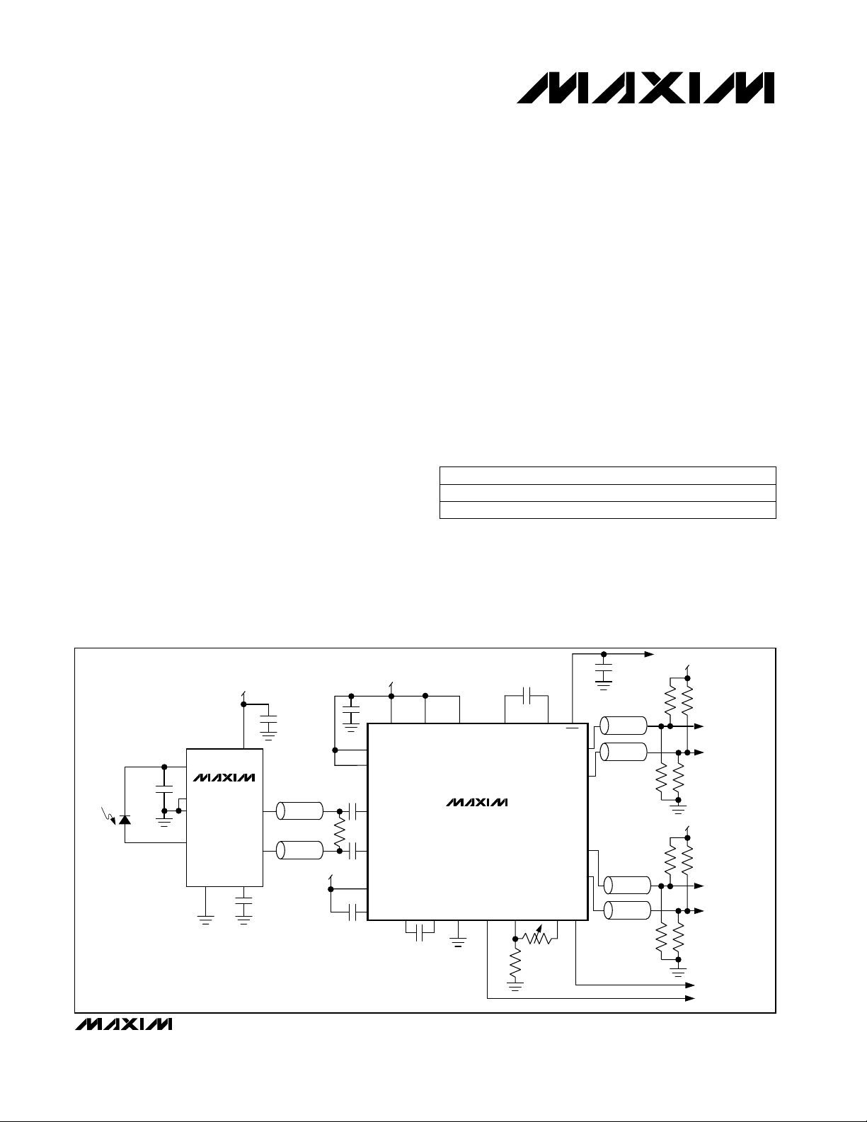
___________________________________________________ Typical Operating Circuit
_____________________ General Description
The MAX3676 is a complete clock-recovery and dataretiming IC incorporating a limiting amplifier. It is intended for 622Mbps SDH/SONET applications and operates
from a single +3.3V supply.
The MAX3676 is designed for both section-regenerator
and terminal-receiver applications in OC12/STM-4 transmission systems. Its jitter performance exceeds all
SONET/SDH specifications.
The MAX3676 has two differential input amplifiers: one
accepts positive-referenced emitter-coupled logic
(PECL) levels, while the other accepts small-signal analog levels. The analog inputs access the limiting amplifier stage, which provides both a received-signal-strength
indicator (RSSI) and a programmable-threshold loss-ofpower (LOP) monitor. Selecting the PECL amplifier disables the limiting amplifier, conserving power. A
loss-of-lock (LOL) monitor is also incorporated as part of
the fully integrated phase-locked loop (PLL).
________________________Applications
SDH/SONET Receivers and Regenerators
SDH/SONET Access Nodes
Add/Drop Multiplexers
ATM Switches
Digital Cross-Connects
____________________________Features
♦ Single +3.3V or +5.0V Power Supply
♦ Exceeds ITU/Bellcore SDH/SONET Regenerator
Specifications
♦ Low Power: 237mW at +3.3V
♦ Selectable Data Inputs, Differential PECL or
Analog
♦ Received-Signal-Strength Indicator
♦ Loss-of-Power and Loss-of-Lock Monitors
♦ Differential PECL Clock and Data Outputs
♦ No External Reference Clock Required
MAX3676
622Mbps, 3.3V Clock-Recovery and
Data-Retiming IC with Limiting Amplifier
________________________________________________________________
Maxim Integrated Products
1
19-1537; Rev 0; 7/99
PART TEMP. RANGE PIN-PACKAGE
_________________Ordering Information
Pin Configuration appears at end of data sheet.
*Contact factory for availability. Dice are designed to operate
over a -40°C to +140°C junction temperature (T
j
) range, but are
tested and guaranteed at Tj= +45°C.
For free samples & the latest literature: http://www.maxim-ic.com, or phone 1-800-998-8800.
For small orders, phone 1-800-835-8769.
MAX3676EHJ
-40°C to +85°C 5mm 32 TQFP
MAX3676E/D -40°C to +85°C Dice*
+3.3V
130Ω 130Ω
82Ω
130Ω 130Ω
82Ω
82Ω
+3.3V
82Ω
100pF
PHOTO-
DIODE
FILT
INREF
IN
GND
MAX3664
+3.3V
V
CC
OUT+
OUT-
COMP
220pF
0.01µF
ZO = 50Ω
ZO = 50Ω
100Ω
+3.3V
C
IN
0.01µF
C
IN
0.01µF
C
47nF
0.1µF
F
+3.3V
PHADJ+ PHADJ-
INSEL
DDI+
DDI-
ADI+
ADI-
V
CC
CFILT OLC+ OLC-
C
OLC
33nF
FIL+
MAX3676
GND
RSSI INV VTH LOP
2.2µF
R1
20k
C
LOL
0.01µF
LOL
FIL-
SDO+
SDO-
SCLKO+
SCLKO-
R2
ZO = 50Ω
ZO = 50Ω
ZO = 50Ω
ZO = 50Ω
MAX3676
622Mbps, 3.3V Clock-Recovery and
Data-Retiming IC with Limiting Amplifier
2 _______________________________________________________________________________________
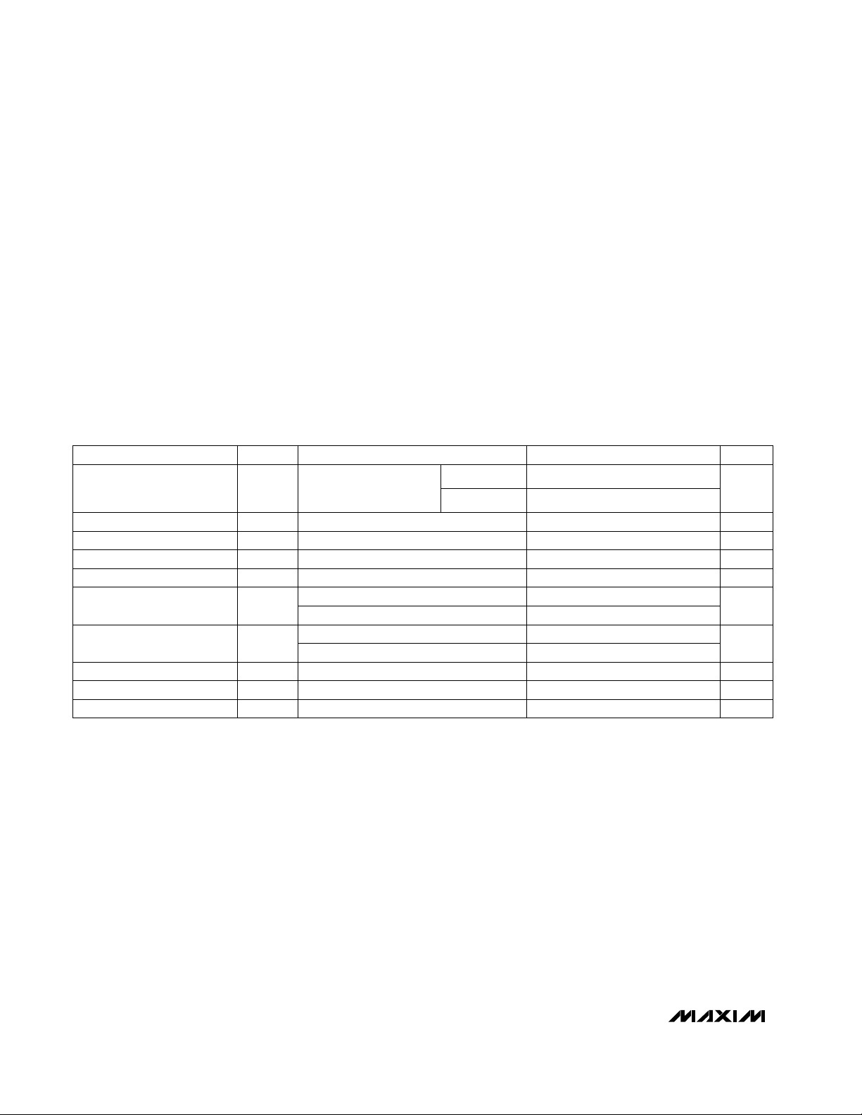
ABSOLUTE MAXIMUM RATINGS
DC ELECTRICAL CHARACTERISTICS
(VCC= +3.0V to +5.5V, TA= -40°C to +85°C, unless otherwise noted. Typical values are at TA= +25°C.) (Notes 1, 2)
Stresses beyond those listed under “Absolute Maximum Ratings” may cause permanent damage to the device. These are stress ratings only, and functional
operation of the device at these or any other conditions beyond those indicated in the operational sections of the specifications is not implied. Exposure to
absolute maximum rating conditions for extended periods may affect device reliability.
Supply Voltage, VCC..............................................-0.5V to +6.5V
Input Voltage Levels,
DDI+, DDI-, ADI+, ADI-...........................-0.5V to (V
CC
+ 0.5V)
Input Differential Voltage (ADI+) - (ADI-)...............................±3V
PECL Output Currents, SDO+, SDO-, SCLKO+, SCLKO-...100mA
LOL, LOP, INSEL, PHADJ+, PHADJ-.........-0.5V to (V
CC
+ 0.5V)
FIL+, FIL-, OLC+, OLC-, RSSI, VTH...........-0.5V to (V
CC
+ 0.5V)
(OLC+) - (OLC-).....................................................................±3V
(FIL+) - (FIL-) ..................................................................±700mV
CFILT...............................................(V
CC
- 2.5V) to (VCC+ 0.5V)
INV.........................................................................-0.5V to +2.0V
Continuous Power Dissipation (T
A
= +85°C)
TQFP (derate 11.1mW/°C above +85°C).....................721mW
Operating Junction Temperature Range...........-40°C to +150°C
Storage Temperature Range .............................-65°C to +150°C
Processing Temperature (die) .........................................+400°C
Lead Temperature (soldering, 10sec) .............................+300°C
MAX3676EHJ,
PECL outputs
unterminated
TA= 0°C to +85°C
TA= 0°C to +85°C
CONDITIONS
VVCC- 1.16 VCC- 0.88V
IH
PECL Input Voltage High
51 81
72 111
V0.1 0.4V
OL
LOP, LOL Voltage Low
V2.4V
OH
LOP, LOL Voltage High
VCC- 1.81 VCC- 1.620
VVCC- 1.81 VCC- 1.48V
IL
PECL Input Voltage Low
µA-10 10I
IH
PECL Input Current High
µA-10 10I
IL
PECL Input Current Low
VCC- 1.025 VCC- 0.88
UNITSMIN TYP MAXSYMBOLPARAMETER
INSEL = V
CC
INSEL = GND
Note 1: Dice are tested at Tj= +45°C, VCC= +4.25V.
Note 2: At T
A
= -40°C, DC characteristics are guaranteed by design and characterization.
mAI
CC
Supply Current
TA= -40°C
V
VCC- 1.085 VCC- 0.88
V
OH
PECL Output Voltage High
TA= -40°C
V
VCC- 1.83 VCC- 1.555
V
OL
PECL Output Voltage Low
4kΩ between INV and VTH V1.10 1.23 1.30INV Input Bias Voltage
MAX3676
622Mbps, 3.3V Clock-Recovery and
Data-Retiming IC with Limiting Amplifier
_______________________________________________________________________________________ 3
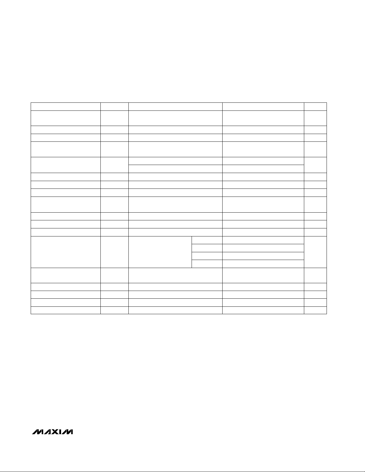
AC ELECTRICAL CHARACTERISTICS
(VCC= +3.0V to +5.5V, TA= -40°C to +85°C, unless otherwise noted. Typical values are at VCC= +3.3V and TA= +25°C.)
(Notes 3, 4)
Note 3: AC parameters are guaranteed by design and characterization.
Note 4: The MAX3676 is characterized with a PRBS of 2
23
- 1 maintaining a BER of ≤ 10
-10
having a confidence level of 99.9%.
Note 5: A lower minimum input voltage of 2mVp-p is achievable; however, the LOP hysteresis is not guaranteed below 3.6mVp-p.
Note 6: Hysteresis = 20log(V
RELEASE
/ V
ASSERT
).
Note 7: R
1
= 20kΩ, R
2 =
3.0kΩ, resulting in V
RELEASE
≈ 3.6mVp-p.
Note 8: Small-signal bandwidth cannot be measured directly.
Note 9: RSSI slope = [V
RSSI2
- V
RSSI1
] / [20log (V
ID2
/ V
ID1
)].
Note 10: 1UI = 1 unit interval = (622.08MHz)
-1
= 1.608ns.
Note 11: At jitter frequencies <10kHz, the jitter tolerance characteristics exceed the ITU/Bellcore specifications. The low-frequency
jitter tolerance outperforms the instrument’s measurement capability.
Note 12: See
Typical Operating Characteristics
for worst-case distribution.
PARAMETER SYMBOL MIN TYP MAX UNITS
RSSI Output Voltage
1.40
Limiting Amplifier SmallSignal Bandwidth
BW
650
MHz
Power-Detect Hysteresis
36
dB
Input-Referred Noise V
N
80
µV
RMS
Threshold Voltage V
TH
1.41
V
Differential Input Voltage
Range
V
ID
0.003 1.2000
Vp-p
CONDITIONS
(ADI+) - (ADI-) = 2mVp-p
(Note 8)
(Notes 6, 7)
ADI inputs
(Note 7)
BER < 10
-10
, ADI inputs (Note 5)
1.93
V
(ADI+) - (ADI-) = 20mVp-p
Jitter-Transfer Peaking
0.03 0.08
dB
Maximum Consecutive Input
Run Length (1 or 0)
1200
Bits
CF= 2.2µF
8.9
CF= 2.2µF
(Note 12) 3.64
Jitter Tolerance (Note 11)
0.55 0.77
0.45 0.69
CF= 2.2µFLoop Bandwidth
250 500
kHz
26
RSSI Linearity
±0.7
%(ADI+) - (ADI-) = 2mVp-p to 50mVp-p
RSSI Slope mV/dB
(ADI+) - (ADI-) = 2mVp-p to 50mVp-p
(Note 9)
UI
f =10kHz
f =25kHz
f = 250kHz
f =1MHz
CF= 2.2µFJitter Generation (Note 10)
2.0 2.6
mUI
LOP Threshold Accuracy
-2 +2
dB(Note 7)
Clock Transition Time tr, tf
205 245
ps20% to 80%
Data Transition Time tr, tf
180 230
ps20% to 80%
Serial Clock-to-Q Delay t
CLK-Q
140 275 400
ps
Serial Clock Frequency f
SCLK
622.08
MHz
MAX3676
622Mbps, 3.3V Clock-Recovery and
Data-Retiming IC with Limiting Amplifier
4 _______________________________________________________________________________________
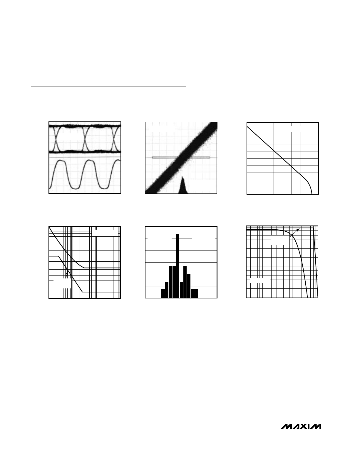
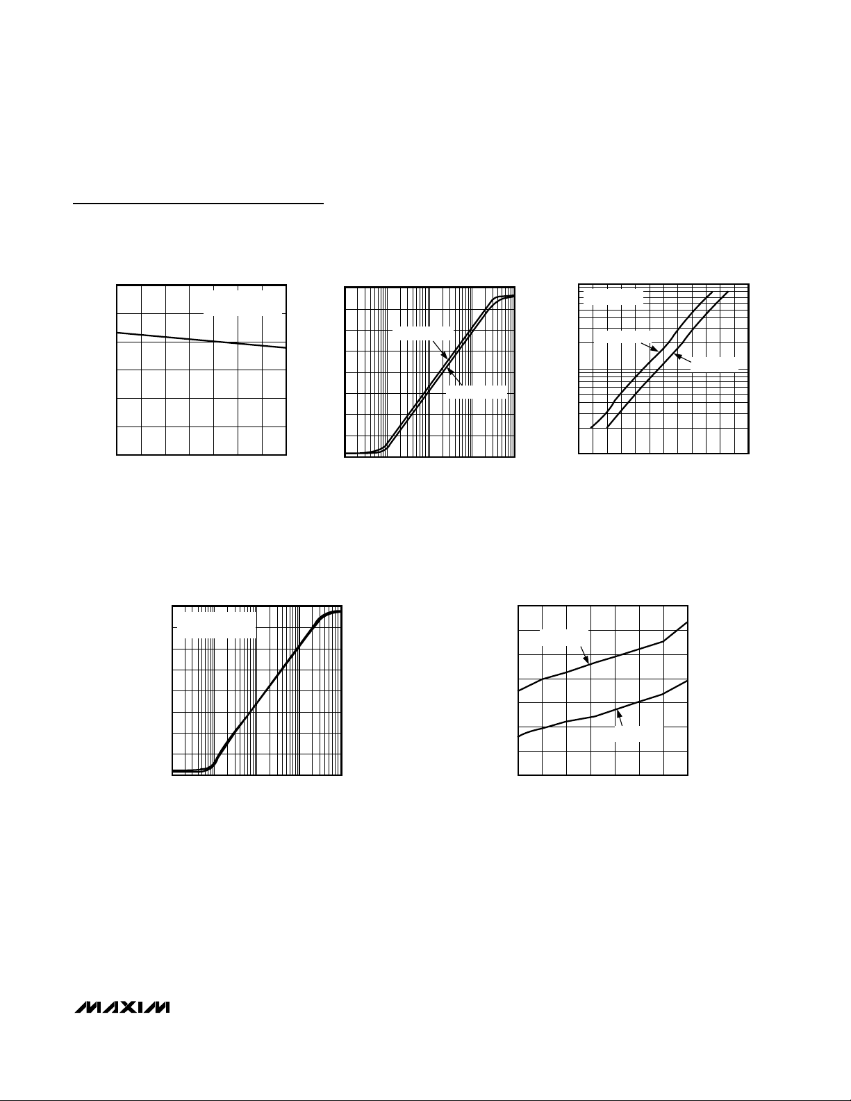
Typical Operating Characteristics
(VCC= +3.3V, TA = +25°C, unless otherwise noted.)
400ps/div
CLOCK
DATA
RECOVERED DATA AND
CLOCK (SINGLE ENDED)
MAX3676 toc01
2
23
-1 PATTERN
20ps/div
RECOVERED CLOCK JITTER
MAX3676 toc02
2
23
-1 PATTERN
WIDEBAND RMS
JITTER = 5.84ps
10
-2
10
-3
10
-4
10
-5
10
-6
10
-7
10
-8
10
-9
10
-10
10
-11
10
-12
600µ500µ400µ 800µ700µ 900µ 1m 1.1m 1.2m
BIT ERROR RATE
vs. ADI INPUT VOLTAGE
MAX3676 toc03
INPUT VOLTAGE (V)
BIT ERROR RATE
2
23
-1 PATTERN
10
0.1
10k 100k 1M 10M
JITTER TOLERANCE
MAX3676 toc04
JITTER FREQUENCY (Hz)
INPUT JITTER (UIp-p)
1
2
23
-1 PATTERN
BELLCORE
MASK
0.2
0
-0.2
-0.4
-0.6
-0.8
-1.0
-1.2
-1.4
-1.6
-1.8
-2.0
-2.2
-2.4
-2.6
-2.8
-3.0
2k 10k 100k 700k
JITTER TRANSFER
MAX3676 toc05
JITTER FREQUENCY (Hz)
JITTER TRANSFER (dB)
2
23
- 1 PRBS
BELLCORE
MASK
0
10
5
20
15
25
30
1.5
2.4
2.0
2.2
3.02.6
2.8
3.5
DISTRIBUTION OF JITTER TOLERANCE
(WORST-CASE CONDITIONS)
MAX3676 toc06
JITTER TOLERANCE (UI
p-p
)
PERCENT OF UNITS (%)
f
JITTER
= 25kHz
V
CC
= +3.0V
T
A
= +85°C
MEAN = 2.42UI
σ = 0.227UI
MAX3676
622Mbps, 3.3V Clock-Recovery and
Data-Retiming IC with Limiting Amplifier
_______________________________________________________________________________________ 5
Typical Operating Characteristics (continued)
(VCC= +3.3V, TA = +25°C, unless otherwise noted.)
2.0
3.0
2.5
3.5
4.0
4.5
5.0
-40 0-20 20 40 60 80 100
LOSS-OF-POWER
HYSTERESIS vs. TEMPERATURE
MAS3676 toc07
AMBIENT TEMPERATURE (°C)
HYSTERESIS (dB)
2
23
-1 PATTERN
V
CC
= +3.3V OR +5.0V
RECEIVED-SIGNAL-STRENGTH INDICATOR
vs. INPUT VOLTAGE
2.7
1.1
0.1 10 1001.0 1000
1.3
1.5
MAX3676 toc08
INPUT VOLTAGE (mVp-p)
RSSI (V)
1.7
1.9
2.1
2.3
2.5
2
23
-1 PATTERN
1010 PATTERN
100
1
1.31.2 2.42.32.22.12.01.91.81.71.61.51.4
LOSS-OF-POWER
ASSERT AND RELEASE LEVEL
vs. DETECTOR THRESHOLD VOLTAGE
MAX3676 toc09
DETECTOR THRESHOLD VOLTAGE, VTH (V)
ANALOG VOLTAGE (mVp-p)
10
LOP RELEASE
LOP ASSERT
2
23
-1 PATTERN
2.7
1.1
0.1 10 1001.0 1000
RECEIVED-SIGNAL-STRENGTH INDICATOR
vs. INPUT VOLTAGE
1.3
1.5
MAX3676 toc10
INPUT VOLTAGE (mVp-p)
RSSI (V)
1.7
1.9
2.1
2.3
2.5
2
23
-1 PATTERN
V
CC
= +3.3V OR +5.0V
30
50
40
70
60
80
90
100
-40 0 20-20 40 60 80 100
SUPPLY CURRENT
vs. TEMPERATURE
MAX3676 toc11
TEMPERATURE (°C)
SUPPLY CURRENT (mA)
V
CC
= +5.0V
V
CC
= +3.3V

MAX3676
622Mbps, 3.3V Clock-Recovery and
Data-Retiming IC with Limiting Amplifier
6 _______________________________________________________________________________________
Pin Description
32 CFILT RSSI Filter Capacitor Input
30 ADI+ Positive Analog Data Input, 622.08Mbps serial-data stream
29 ADI- Negative Analog Data Input, 622.08Mbps serial-data stream
28 INSEL Input Select. Connect to GND to select digital data inputs or VCCfor analog data inputs.
27 DDI- Negative Digital Data Input, PECL, 622.08Mbps serial-data stream
26 DDI+ Positive Digital Data Input, PECL, 622.08Mbps serial-data stream
23 FIL+ Positive Filter Input. PLL loop filter connection.
22 FIL- Negative Filter Input. PLL loop filter connection.
20 PHADJ+ Positive Phase-Adjust Input. Used to optimally align internal PLL phase. Attach to VCCif not used.
19 PHADJ- Negative Phase-Adjust Input. Used to optimally align internal PLL phase. Attach to VCCif not used.
NAME FUNCTION
1 OLC+ Positive Offset-Correction Loop Capacitor Input
2 OLC- Negative Offset-Correction Loop Capacitor Input
PIN
3 RSSI Received-Signal-Strength Indicator Output
4, 8, 16,
24, 25
GND Supply Ground
9, 12, 15,
18, 21, 31
V
CC
Positive Supply Voltage
7 LOP
Loss-of-Power Output, TTL. Limiting amplifier loss-of-power monitor. Asserts high when input signal
is below threshold set by VTH.
6 VTH
Voltage Threshold Input. Threshold voltage for loss-of-power monitor. Attach to VCCif LOP function
is not used.
5 INV Op Amp Inverting Input. Attach to ground if op amp is not used.
17
LOL
Loss-of-Lock Output, TTL. PLL loss-of-lock monitor, active low (see
Design Procedure
).
14 SDO+ Positive Serial-Data Output, PECL, 622.08Mbps
13 SDO- Negative Serial-Data Output, PECL, 622.08Mbps
11 SCLKO+ Positive Serial-Clock Output, PECL, 622.08MHz. SDO+ is clocked out on the rising edge of SCLKO+.
10 SCLKO- Negative Serial-Clock Output, PECL, 622.08MHz. SDO- is clocked out on the falling edge of SCLKO-.

MAX3676
622Mbps, 3.3V Clock-Recovery and
Data-Retiming IC with Limiting Amplifier
_______________________________________________________________________________________ 7
_______________Detailed Description
The block diagram in Figure 1 shows the MAX3676’s
architecture. It consists of a limiting-amplifier input
stage followed by a fully integrated clock/data-recovery
(CDR) block implemented with a PLL. The input stage
is selectable between a limiting amplifier or a simple
PECL input buffer. The limiting amplifier provides an
LOP monitor and an RSSI output. The PLL consists of a
phase/frequency detector (PFD), a loop filter amplifier,
and a voltage-controlled oscillator (VCO).
Limiting Amplifier
The MAX3676’s on-chip limiting amplifier accepts an
input signal level from 3.0mVp-p to 1.2Vp-p. The amplifier consists of a cascade of gain stages that include
full-wave logarithmic detectors. The combined smallsignal gain is approximately 42dB, and the -3dB bandwidth is 650MHz. Input-referred noise is typically
80µV
RMS
, providing excellent sensitivity for small-ampli-
tude data streams.
In addition to driving the CDR, the limiting amplifier pro-
vides both an RSSI output and an LOP monitor that
allow the user to program the threshold voltage. The
RSSI circuitry provides an output voltage that is linearly
proportional to the input power (in decibels) detected
between the ADI+ and ADI- input pins and is sensitive
enough to reliably detect signals as small as 2mVp-p
(see
Typical Operating Characteristics
).
Input DC offset reduces the accuracy of the power
detector; therefore, an integrated feedback loop is
included that automatically nulls the input offset of the
gain stage. The addition of this offset-correction loop
requires that the input signal be AC-coupled when
using the ADI+ and ADI- inputs.
Finally, for applications that do not require the limiting
amplifier, selecting the digital inputs conserves power
by turning off the postamplifier block.
Figure 1. Functional Diagram
PHADJ-
LOL
V
CC
FIL+ FIL-PHADJ+
DDI+
DDI-
INSEL
ADI-
ADI+
PECL
LIMITER
42dB
CORRECTION
OLC+ OLC-
OFFSET
6k
PHASE/FREQ
DETECTOR
1.23V
BIAS
POWER
DETECT
CFILT RSSI INV VTH LOP
Σ
FILTER
PECL
PECL
SDO+
SDO-
SCLKO+
SCLKO-
DQ
I
VCO
622.08MHz
V
CC
6k
Q
MAX3676

MAX3676
622Mbps, 3.3V Clock-Recovery and
Data-Retiming IC with Limiting Amplifier
8 _______________________________________________________________________________________
Phase Detector
The phase detector produces a voltage proportional to
the phase difference between the incoming data and
the internal clock. Because of its feedback nature, the
PLL drives the error voltage to zero, aligning the recovered clock to the incoming data. The external phase
adjustment pins (PHADJ+, PHADJ-) allow the user to
vary the internal phase alignment.
Frequency Detector
The frequency detector incorporated into the PLL uses
the input data stream edges to sample the quadrature
components of the VCO clock. This generates a difference frequency that aids acquisition during start-up.
Depending on the polarity of the difference frequency,
the PFD drives the VCO so that the difference frequency is reduced to zero. Once frequency acquisition is
obtained, the frequency detector returns to a neutral
state.
Loop Filter and VCO
The VCO is fully integrated, while the loop filter requires
an external R-C network. This filter network determines
the bandwidth and peaking of the second-order PLL.
__________________Design Procedure
Received-Signal-Strength Indicator
The RSSI output voltage is insensitive to temperature
and supply fluctuations. The power detector functions
as a broadband power meter that detects the total RMS
power of all signals within the detector bandwidth
(including input signal noise). The RSSI voltage varies
linearly (in decibels) for inputs of 2mVp-p to 50mVp-p.
The slope over this input range is approximately
26mV/dB.
The high-speed RSSI signal is filtered to an RMS level
with one external capacitor tied from CFILT to VCC. The
impedance looking into CFILT is about 500Ω to VCC. As
a result, the lower -3dB cutoff frequency is set by the
following simple relationship:
For 622Mbps applications, Maxim recommends a cutoff frequency of 6.8kHz, which requires CF= 47nF. The
RSSI output is designed to drive a minimum load resistance of 100kΩ to ground and a maximum of 20pF.
Loads greater than 20pF must be buffered by a series
resistance of 100kΩ (i.e., voltmeter).
Input Offset Correction
The on-chip limiting amplifier provides more than 42dB
of gain. A low-frequency feedback loop is integrated
into the MAX3676 to remove the input offset. DC-coupling to the ADI+ and ADI- inputs is not allowed, as this
would prevent the proper functioning of the DC offsetcorrection circuitry.
The differential input impedance (Z
IN
) is approximately
2.5kΩ. The impedance between OLC+ and OLC- (Z
OLC
)
is approximately 120kΩ. Take care when setting the
combined low-frequency cutoff (f
CUTOFF
), due to the
input DC-blocking capacitor (CIN) and the offset correction loop capacitor (C
OLC
). See Table 1 for selecting the
values of CINand C
OLC
.
These values ensure that the poles associated with C
IN
and C
OLC
work together to provide a flat response at the
lower -3dB corner frequency (no gain peaking).
CINmust be a low-TC, high-quality capacitor of type X7R
or better in order to minimize f
CUTOFF
deviations. C
OLC
must be a capacitor of type Z5U or better.
Loss-of-Power Monitor
An LOP monitor with a user-programmable threshold
and a hysteresis comparator is also included with the
limiting amplifier circuitry. Internally, one comparator
input is tied to the RSSI output signal, and the other is
tied to the threshold voltage (VTH), which is set externally and provides a trip point for the LOP indication. A
low-voltage, low-drift op amp, referenced to an internal
bandgap voltage (1.23V), is supplied for programming
a supply independent threshold voltage. This op amp
requires two external resistors to program the LOP trip
point. VTHis programmable from 1.23V to 2.6V using
the equation:
The op amp can source only 100µA of current.
Therefore, an R1 value of 20kΩ is recommended for
proper operation. The input bias current of the op amp
at the INV pin is less than ±100nA.
C
OLC
COMBINED LOW
f
CUTOFF
(kHz)
2200pF 0.015µF 29
1000pF 0.01µF 68
C
IN
470pF 3300pF 135
330pF 2200pF 190
220pF 1500pF 290
Table 1. Setting the Low-Frequency Cutoff
4700pF 0.033µF 13.5
6800pF 0.082µF 10
0.010µF 0.1µF 6.8
0.022µF 0.15µF 3.0
f = 1 / 2 500
FILT
π
()
[]
C
F
V = 1.23 1 + R2 / R1
TH
()

MAX3676
622Mbps, 3.3V Clock-Recovery and
Data-Retiming IC with Limiting Amplifier
_______________________________________________________________________________________ 9
The comparator is configured with an active-high LOP
output. An on-chip, 6kΩ pull-up resistor is provided to
reduce the external part count.
Setting the Loop Filter
The MAX3676 is designed for both regenerator and
receiver applications. Its fully integrated PLL is a classic
second-order feedback system, with a loop bandwidth
(fL) fixed at 250kHz. The external capacitor, CF, can be
adjusted to set the loop damping. Figures 2 and 3 show
the open-loop and closed-loop transfer functions. The
PLL zero frequency, fZ, is a function of external capacitor CF, and can be approximated according to:
For an overdamped system (fZ/fL) <0.25, the jitter peaking (MP) of a second-order system can be approximated by:
For example, using CF= 0.22µF results in a jitter peaking of 0.27dB. Reducing CFbelow 0.22µF may result in
PLL instability. The recommended value for CFis 2.2µF
to guarantee a maximum jitter peaking of less than
0.1dB.
The MAX3676 is optimally designed to acquire lock and
to provide a bit-error rate (BER) of less than 10
-1 0
for
long strings of consecutive zeros and ones. Measured
results show that the MAX3676 can tolerate 1200 consecutive ones or zeros. Decreasing CFreduces the
number of tolerated consecutive identical zeros and
ones. CFmust be a low-TC, high-quality capacitor of
type X7R or better.
Lock Detect
The MAX3676’s LOL monitor indicates when the PLL is
locked. Under normal operation, the loop is locked and
the LOL output signal is high. When the MAX3676 loses
lock, a fast negative-edge transition occurs on LOL.
The output level remains at a low level (held by C
LOL
)
until the loop reacquires lock (Figure 4).
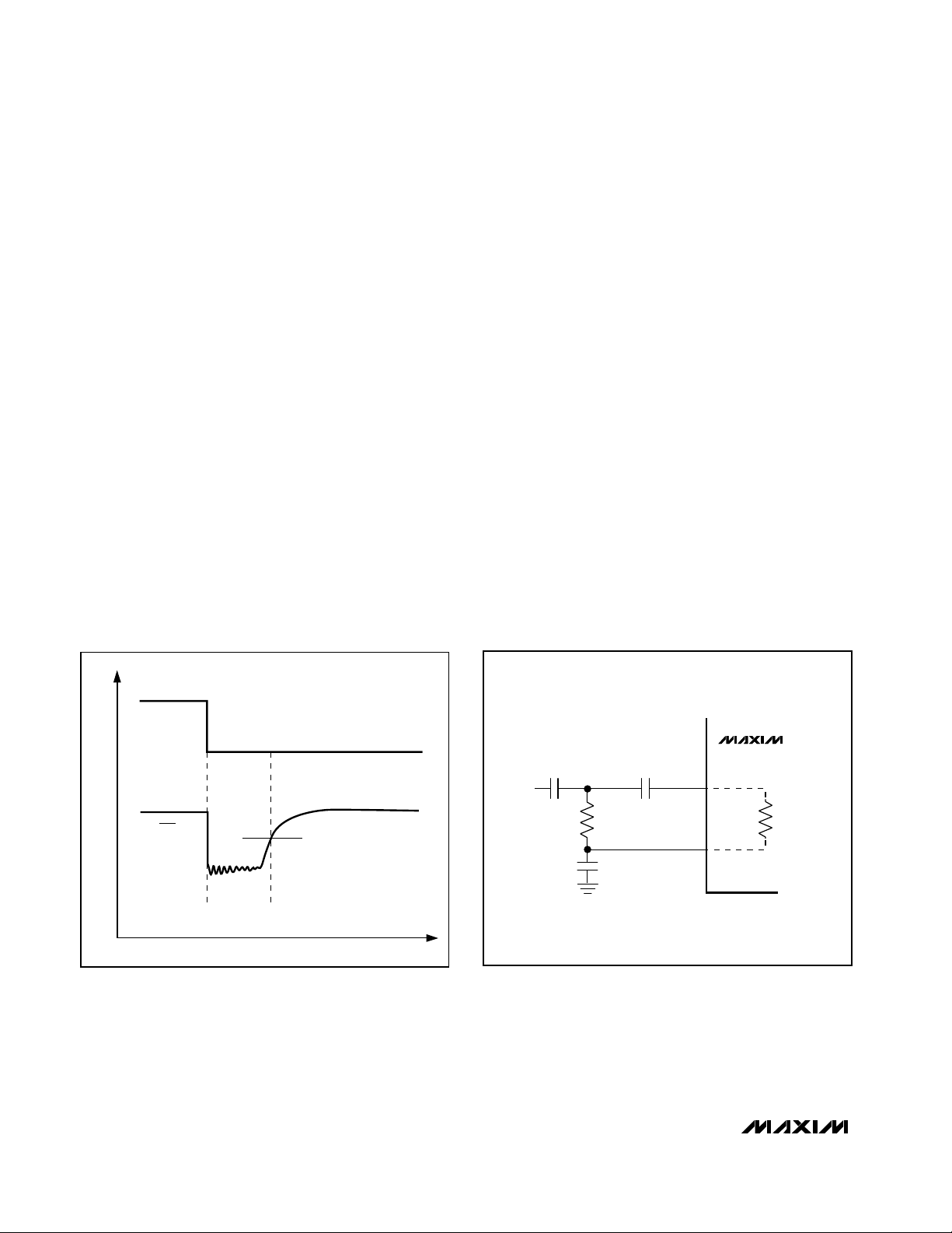
Figure 2. Open-Loop Transfer Function
Figure 3. Closed-Loop Transfer Function
f =
Z
2
π() 90 C
1
F
M = 0log 1+
P
2
f
Z
f
L
C
= 2.2µF
F
OPEN-LOOP GAIN
f
= 804Hz
Z
100 1k 10k 100k
H(J2πf) (dB)
0
-3
CLOSED-LOOP GAIN
100 1k 10k 100k
C
= 0.22µF
F
= 8.04kHz
f
Z
C
C
= 2.2µF
F
= 0.22µF
F
f (Hz)
1M 10M
f (kHz)
1M 10M
MAX3676
622Mbps, 3.3V Clock-Recovery and
Data-Retiming IC with Limiting Amplifier
10 ______________________________________________________________________________________
Note that the LOL monitor is only valid when a data
stream is present on the inputs to the MAX3676. As a
result, LOL does not detect a loss-of-power condition
resulting from a loss of the incoming signal. See the
Loss-of-Power Monitor
section for this type of indicator.
Input and Output Terminations
The MAX3676 digital data and clock I/Os (DDI+, DDI-,
SDO+, SDO-, SCLK+, and SCLK-) are designed to
interface with PECL signal levels. It is important to bias
these ports appropriately. A circuit that provides a
Thevenin equivalent of 50Ω to VCC- 2V should be used
with fixed-impedance transmission lines for proper termination. Make sure that the differential outputs have
balanced loads.
The digital data input signals (DDI+ and DDI-) are differential inputs to an emitter-coupled pair. As a result,
the MAX3676 can accept differential input signals as
low as 250mV. These inputs can also be driven singleended by externally biasing DDI- to the center of the
voltage swing.
The MAX3676’s performance can be greatly affected
by circuit board layout and design. Use good high-fre-
quency design techniques, including minimizing
ground inductance and using fixed-impedance transmission lines on the data and clock signals. Power-supply decoupling should be placed as close to V
CC
as
possible. Take care to isolate the input from the output
signals to reduce feedthrough.
__________Applications Information
Driving the Limiting Amplifier
Single-Ended
There are three important requirements for driving the
limiting amplifier from a single-ended source (Figure 5):
1) There must be no DC-coupling to the ADI+ and ADI-
inputs. DC levels at these inputs disrupt the offsetcorrection loop.
2) The terminating resistor RT(50Ω) must be referenced
to the ADI- input to minimize common-mode coupling
problems.
3) The low-frequency cutoff for the limiting amplifier
is determined by either CINand the 2.5kΩ input
impedance or Cb/2 together with RT. With Cb= 0.22µF
and RT= 50Ω, the low-frequency cutoff is 29kHz.
Figure 4. Loss-of-Lock Output
Figure 5. Single-Ended Input Termination
LOP
C
b
0.22µF
OUTPUT LEVEL
LOL
ACQUIRENO DATA
LOCKED
TIME
R
T
50Ω
C
b
0.22µF
C
5.6nF
IN
ADI+
ADI-
MAX3676
2.5k

MAX3676
622Mbps, 3.3V Clock-Recovery and
Data-Retiming IC with Limiting Amplifier
______________________________________________________________________________________ 11
Reduced Power Consumption
Without the Limiting Amplifier
The limiting amplifier is biased independently from the
clock recovery circuitry. Grounding INSEL turns off the
limiting amplifier and selects the PECL DDI inputs.
Converting Average Optical Power
to Signal Amplitude
Many of the MAX3676’s specifications relate to inputsignal amplitude. When working with fiber optic
receivers, the input is usually expressed in terms of
average optical power and extinction ratio. The relations given in Table 2 and Figure 6 are helpful for converting optical power to input signal when designing
with the MAX3676.
In an optical receiver, the input voltage to the limiting
amplifier can be found by multiplying the relationship in
Table 2 by the photodiode responsivity and transimpedance amplifier gain.
Optical Hysteresis
Power and hysteresis are often expressed in decibels.
By definition, decibels are always 10log (power). At the
inputs to the MAX3676 limiting amplifier, the power is
V
IN
2
/R. If a receiver’s optical input power (x) increases
by a factor of two, and the preamplifier is linear, then the
voltage at the input to the MAX3676 also increases by a
factor of two.
The optical power increase is:
10log(2x /x) = 10log(2) = +3dB
At the MAX3676, the voltage increase is:
In an optical receiver, the decibel change at the
MAX3676 always equals 2x the optical decibel change.
The MAX3676’s typical voltage hysteresis is 3.0dB. This
provides an optical hysteresis of 1.5dB.
Jitter in Optical Receivers
Timing jitter, edge speeds, aberrations, optical dispersion, and attenuation all impact the performance of
high-speed clock recovery for SDH/SONET receivers
(Figure 7). These effects decrease the time available
for error-free data recovery by reducing the received
“eye opening” of nonreturn-to-zero (NRZ) transmitted
signals.
10 10 2 20 2 6
2
2
2
log log( ) log( )
2V / R
V/ R
IN
IN
()
===+dB
Figure 6. Optical Power Relations
Table 2. Optical-Power Relations*
*Assuming a 50% average input-data duty cycle
SYMBOL RELATION
Average
Power
P
AVG
Extinction
Ratio
r
e
PARAMETER
Optical Power
of a “1”
P1
Optical Power
of a “0”
P0
Signal
Amplitude
P
IN
Figure 7. Eye Diagram With and Without Timing Jitter
P1
P
AVE
P0
TIME
P = P0 + P1 / 2
AVG
()
r = 1 / P0
P
e
PP
121=
AVG
P0 2P / r 1
=+
AVG e
PPPP
=−=
102
IN AVG
r
e
+
r
e
()
r
−
1
()
e
r
+
1
e
AMPLITUDE
EYE DIAGRAM WITH NO TIMING JITTER
AMPLITUDE
EFFECTS OF TIMING JITTER ON EYE DIAGRAM TIME
MIDPOINT
TIME
MIDPOINT

MAX3676
622Mbps, 3.3V Clock-Recovery and
Data-Retiming IC with Limiting Amplifier
12 ______________________________________________________________________________________
Optical receivers, incorporating transimpedance
preamplifiers and limiting postamplifiers, can significantly clean up the effects of dispersion and attenuation. In addition, these amplifiers can provide fast
transitions with minimal aberrations to the subsequent
CDR blocks. However, these stages also add distortions to the midpoint crossing, contributing to timing jitter. Timing jitter is one of the most critical technical
issues to consider when developing optical receivers
and CDR circuits.
A better understanding of the different sources of jitter
helps in the design and application of optical receiver
modules and integrated CDR solutions. SDH/SONET
specifications are well defined regarding the amount of
jitter tolerance allowed at the inputs of optical receivers,
as well as jitter peaking requirements, but they do little
to define the different sources of jitter. The jitter that
must be tolerated at an optical receiver input involves
three significant sources, all of which are present in
varying degrees in typical receiver systems:
1) Random jitter (RJ)
2) Pattern-dependent jitter (PDJ)
3) Pulse-width distortion (PWD)
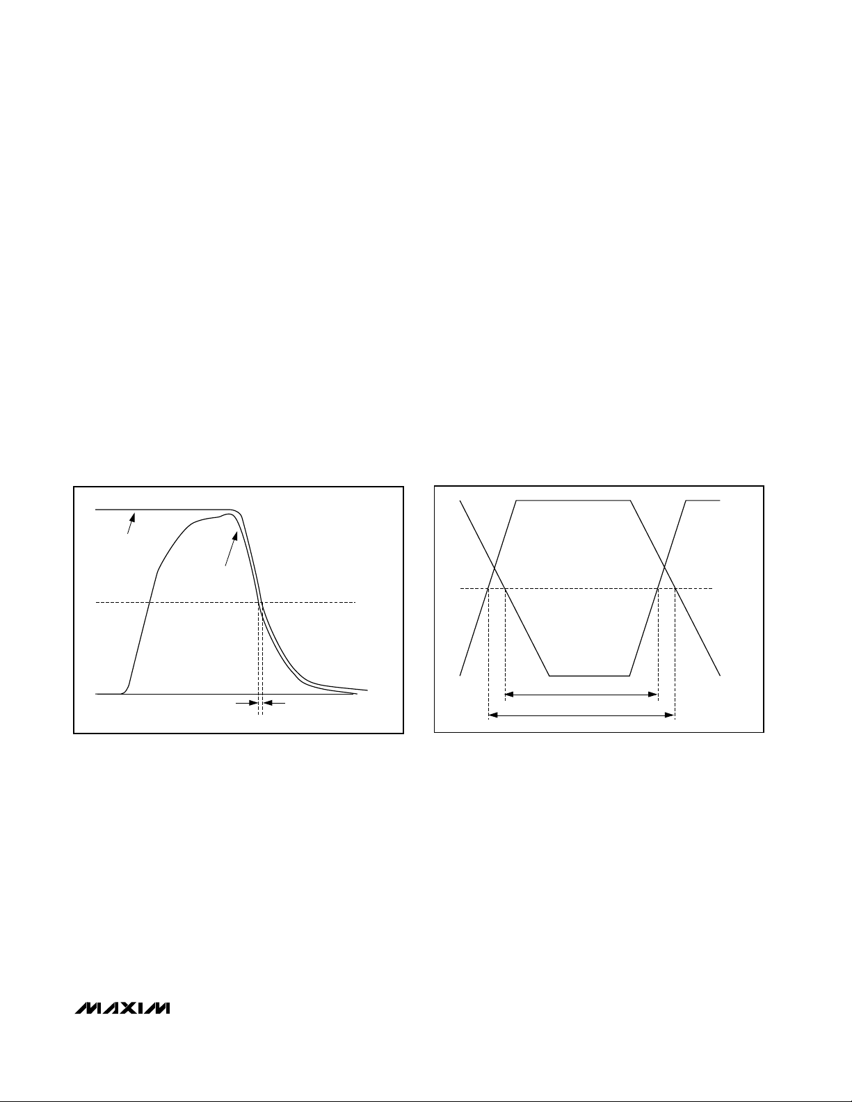
Random Jitter
RJ is caused by random noise present during edge
transitions (Figure 8). This random noise results in random midpoint crossings. All electrical systems generate some random noise; however, the faster the speed
of the transitions, the lower the effect of noise on random jitter. The following equation is a simple worstcase estimation of random jitter:
RJ (rms) = (rms noise) / (slew rate)
Pattern-Dependent Jitter
PDJ results from wide variations in the number of consecutive bits contained in NRZ data streams working
against the bandwidth requirements of the receiver
(Figure 9). The location of the lower -3dB cutoff frequency is important, and must be set to pass the low
frequencies associated with long consecutive bit
streams. AC-coupling is common in optical receiver
design.
When using a preamplifier with a highpass frequency
response, select the input AC-coupling capacitor, CIN,
to provide a low-frequency cutoff (fC) one decade lower
than the preamplifier low-frequency cutoff. As a result,
the PDJ is dominated by the low-frequency cutoff of
the preamplifier.
When using a preamplifier without a highpass response
with the MAX3676, the following equation provides a
good starting point for choosing CIN:
where t
L
= duration of the longest run of consecutive
bits of the same value (seconds); PDJ = maximum
Figure 8. Random Jitter on Edge Transition
Figure 9. Pattern-Dependent Jitter Due to Low-Frequency
Cutoff
C
≥
IN
1.25k In
()
Ω .1
-t
L
PDJ BW
()()
−
05
DESIRED
MIDPOINT
CROSSING
MIDPOINT
ACTUAL
MIDPOINT
CROSSING
RANDOM
JITTER
0–1
TRANSITION
WITH RANDOM
NOISE
MIDPOINT
TIME
AMPLITUDE
LONG
CONSECUTIVE
BIT STREAM
AMPLITUDE
LF DROOP
0-1-0 BIT STREAM
LF PDJ
MIDPOINT
TIME
MAX3676
622Mbps, 3.3V Clock-Recovery and
Data-Retiming IC with Limiting Amplifier
______________________________________________________________________________________ 13
allowable pattern-dependent jitter, peak-to-peak
(seconds); and BW = typical system bandwidth, normally 0.6 to 1.0 times the data rate (Hertz). If the PDJ is
still larger than desired, continue increasing the value of
CIN. Note that to maintain stability when using the
MAX3676 analog inputs (ADI+, ADI-), it is important to
keep the low-frequency cutoff associated with C
OLC
below the corner frequency associated with CIN(fC)
(Table 1).
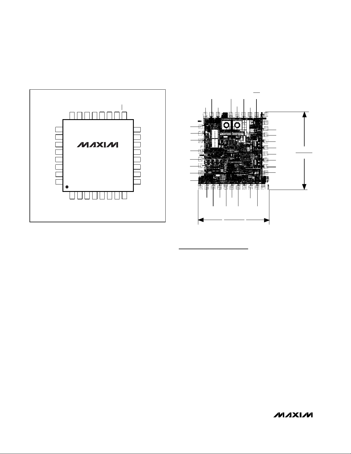
PDJ can also be present due to insufficient high-frequency bandwidth (Figure 10). If the amplifiers are not
fast enough to allow for complete transitions during single-bit patterns, or if the amplifier does not allow adequate settling time, high-frequency PDJ can result.
Pulse-Width Distortion
Finally, PWD occurs when the midpoint crossing of a
0–1 transition and a 1–0 transition does not occur at the
same level (Figure 11). DC offsets and nonsymmetrical
rising and falling edge speeds both contribute to PWD.
For a 1–0 bit stream, calculate PWD as follows:
PWD = [(width of wider pulse) -
(width of narrower pulse)] / 2
Phase Adjust
The internal clock and data alignment in the MAX3676
is well maintained close to the center of the data eye.
Although not required, this sampling point can be shifted using the PHADJ inputs to optimize BER performance. The PHADJ inputs operate with differential
input signals to approximately ±1V. A simple resistor
divider with a bypass capacitor is sufficient to set up
these levels. When the PHADJ inputs are not used, they
should be tied directly to VCC.
Figure 10. Pattern-Dependent Jitter Due to High-Frequency
Rolloff
Figure 11. Pulse-Width Distortion
LONG
CONSECUTIVE
BIT STREAM
AMPLITUDE
0-1-0 BIT STREAM
MIDPOINT
PWD RESULTS WHEN THE WIDTH
OF A ZERO DOES NOT EQUAL
THE WIDTH OF A ONE.
MIDPOINT
AMPLITUDE
t
FALL
≠ t
RISE
HF PDJ
TIME
WIDTH OF A ZERO
WIDTH OF A ONE
TIME
MAX3676
622Mbps, 3.3V Clock-Recovery and
Data-Retiming IC with Limiting Amplifier
14 ______________________________________________________________________________________
__________________Pin Configuration
___________________Chip Topography
Chip Information
TRANSISTOR COUNT: 2528
TOP VIEW
PHADJ+
5
INV
CC
PHADJ-
V
191817
6
7
VTH
LOP
LOL
16
15
14
13
12
11
10
9
8
GND
25
GND
DDI+
DDI-
INSEL
ADI-
ADI+
V
CFILT
26
27
28
29
30
31
CC
32
CC
FIL+
GND
FIL-
V
2423222120
MAX3676
1
2
3
4
GND
RSSI
OLC-
OLC+
TQFP
GND
V
CC
SDO+
SDO-
V
CC
SCLKO+
SCLKO-
V
CC
GND
DDI+
DDI-
INSEL
ADI-
ADI+
V
CFILT
FIL+ V
GND FIL- V
CC
OLC+ RSSI INV
OLC- GND VTH GND
CC
PHADJ+
0.076"
(1.930mm)
PHADJ-
LOP
LOL
CC
GND
V
CC
SDO+
SDO-
V
SCLKO+
SCLKO-
V
CC
CC
0.083"
(2.108mm)

MAX3676
622Mbps, 3.3V Clock-Recovery and
Data-Retiming IC with Limiting Amplifier
______________________________________________________________________________________ 15
________________________________________________________Package Information
32L/48L,TQFP.EPS

MAX3676
622Mbps, 3.3V Clock-Recovery and
Data-Retiming IC with Limiting Amplifier
Maxim cannot assume responsibility for use of any circuitry other than circuitry entirely embodied in a Maxim product. No circuit patent licenses are
implied. Maxim reserves the right to change the circuitry and specifications without notice at any time.
16
____________________Maxim Integrated Products, 120 San Gabriel Drive, Sunnyvale, CA 94086 408-737-7600
© 1999 Maxim Integrated Products Printed USA is a registered trademark of Maxim Integrated Products.
NOTES
 Loading...