

Page 1
General Description
The MAX3668 is a complete, +3.3V laser driver with
automatic power control (APC) circuitry for SDH/SONET
applications up to 622Mbps. It accepts differential
PECL inputs, provides bias and modulation currents,
and operates over a temperature range of -40°C to
+85°C.
An APC feedback loop is incorporated to maintain a
constant average optical power over temperature and
lifetime. The wide modulation current range of 5mA to
75mA and bias current of 1mA to 80mA are easy to
program, making this product ideal for use in various
SDH/SONET applications.
The MAX3668 also provides enable control and a failuremonitor output to indicate when the APC loop is unable
to maintain the average optical power. The MAX3668 is
available in a 5mm 32-pin TQFP package as well as in
dice.
Applications
622Mbps SDH/SONET Access Nodes
Laser Driver Transmitters
Section Regenerators
Features
♦ Single +3.3V or +5.0V Operation
♦ 38mA Supply Current at +3.3V
♦ Programmable Modulation Current from
5mA to 75mA
♦ Programmable Bias Current from 1mA to 80mA
♦ Rise/Fall Time <200ps
♦ Automatic Average Power Control with Failure
Monitor
♦ Complies with ANSI, ITU, and Bellcore
SONET/SDH Specifications
♦ Enable Control
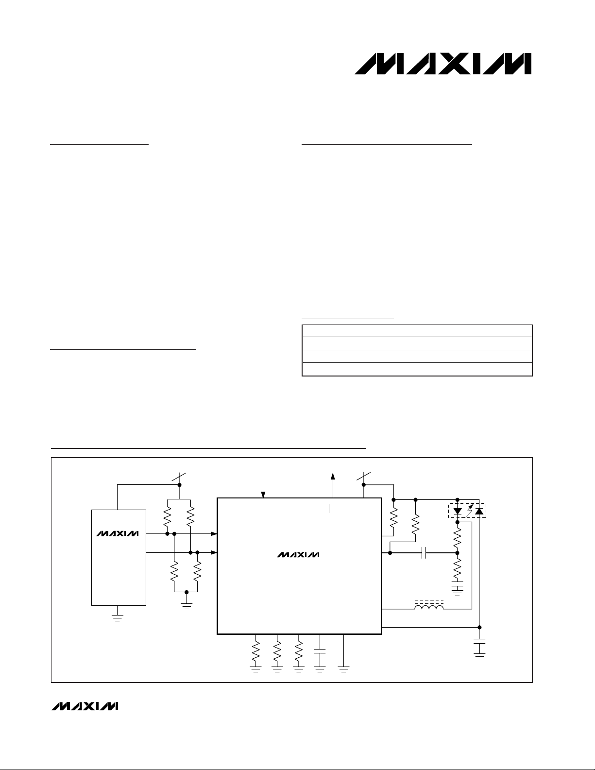
MAX3668
†
+3.3V, 622Mbps SDH/SONET
Laser Driver with Automatic Power Control
________________________________________________________________ Maxim Integrated Products 1
DATA+
BIASMAX
MODSET
APCSET
CAPC
FAIL
ENABLE
GND
MD
BIAS
OUT+
0.1µF
LASER
OUT-
C
MD
1000pF
R
FILT
20Ω
C
FILT
5pF
C
D
1.0µF
R+
20Ω
R-
6.3Ω
R
D
5Ω
FERRITE
BEAD
V
CC
DATA-
PECL
+3.3V +3.3V
82Ω
82Ω
130Ω
130Ω
4:1
SERIALIZER
WITH
CLOCK GEN
MAX3693
MAX3668
Typical Operating Circuit
19-4799; Rev 4; 2/05
Ordering Information
Pin Configuration appears at end of data sheet.
Note: Dice are designed to operate over a -40°C to +140°C
junction temperature (Tj) range, but are tested and guaranteed
at T
A
= +25°C.
*Contact factory for availability.
+Denotes lead-free package.
†
Covered by U.S. Patent numbers 5,802,089 and 5,883,910
For pricing, delivery, and ordering information, please contact Maxim/Dallas Direct! at
1-888-629-4642, or visit Maxim’s website at www.maxim-ic.com.
PART
TEMP RANGE
PIN-PACKAGE
MAX3668EHJ
-40°C to +85°C
32 TQFP (5mm x 5mm)
MAX3668EHJ+
-40°C to +85°C
32 TQFP (5mm x 5mm)
MAX3668E/D
Note
Dice*
Page 2
MAX3668
+3.3V, 622Mbps SDH/SONET
Laser Driver with Automatic Power Control
2 _______________________________________________________________________________________
ABSOLUTE MAXIMUM RATINGS
DC ELECTRICAL CHARACTERISTICS
(VCC= +3.14V to +5.5V, TA= -40°C to +85°C, unless otherwise noted. Typical values are at VCC= +3.3V, TA= +25°C.) (Note 1)
Stresses beyond those listed under “Absolute Maximum Ratings” may cause permanent damage to the device. These are stress ratings only, and functional
operation of the device at these or any other conditions beyond those indicated in the operational sections of the specifications is not implied. Exposure to
absolute maximum rating conditions for extended periods may affect device reliability.
Supply Voltage, VCC.............................................-0.5V to +7.0V
Current into BIAS ............................................-20mA to +150mA
Current into OUT+, OUT- ............................... -20mA to +100mA
Current into MD....................................................-5mA to +5mA
Voltage at DATA+, DATA-, ENABLE,
FAIL .......................................................-0.5V to (VCC+ 0.5V)
Voltage at OUT+, OUT-.............................+1.5V to (V
CC
+ 1.5V)
Voltage at MODSET, APCSET, BIASMAX,
CAPC............................................................... -0.5V to +3.0V
Voltage at BIAS .........................................+1.0V to (V
CC
+ 0.5V)
Continuous Power Dissipation (T
A
= +85°C)
32-Pin TQFP (derate 14.3mW/°C above +85°C)........ 929mW
Operating Junction Temperature Range...........-55°C to +150°C
Processing Temperature (Die).........................................+400°C
Storage Temperature Range ........................... -65°C to +165°C
Lead Temperature (soldering, 10s) ................................+300°C
ENABLE = low (Note 3)
V
BIAS
= V
CC
- 1.6V
(Note 2)
Sinking 100µA
Sourcing 50µA
(Note 4)
APC open loop
APC open loop
Figure 1
PECL compatible
CONDITIONS
V0.1 0.44V
OL
TTL Output Low Voltage
(FAIL)
V2.4 V
CC
- 0.3 V
CC
V
OH
TTL Output High Voltage
(FAIL)
V0.8V
IL
TTL Input Low Voltage
V2.0V
IH
TTL Input High Voltage
V0.8V
MD
Monitor Diode Input Voltage
(MD Pin)
µA100Bias Off Current
mA180I
BIAS
mA38 60Supply Current
Bias Current Range
µA18 1000I
MD
DC Monitor Diode Current
%-15 15
Monitor Diode Current
Absolute Accuracy
ppm/°C
-480 10 480
Monitor Diode Current Stability
µA-1 10I
IN
DATA+, DATA- Input Current
ppm/°C
390
Bias Current Stability
%-15 15Bias Current Absolute Accuracy
mVp-p200 1600V
ID
Differential Input Voltage
V
V
CC
-V
CC
-V
CC
-
1.49 1.32 V
ID
/4
V
ICM
Common-Mode Input Voltage
UNITSMIN TYP MAXSYMBOLPARAMETER
I
BIAS
= 80mA
I
BIAS
= 1mA 920
IMD= 1mA
IMD= 18µA (Note 5) 70
Page 3
MAX3668
+3.3V, 622Mbps SDH/SONET
Laser Driver with Automatic Power Control
_______________________________________________________________________________________ 3
AC ELECTRICAL CHARACTERISTICS
(VCC= +3.14V to +5.5V, load as shown in Figure 2, TA= -40°C to +85°C, unless otherwise noted. Typical values are at VCC= +3.3V,
T
A
= +25°C.) (Note 6)
Note 1: Characteristics at -40°C are guaranteed by design and characterization. Dice are tested at TA= +25°C only.
Note 2: Tested with R
MODSET
= 5.11kΩ (I
MOD
≈ 38mA), R
BIASMAX
= 4.56kΩ (I
BIAS
≈ 52mA), excluding I
BIAS
and I
MOD
.
Note 3: Both the bias and modulation currents will be disabled if any of the current set pins are shorted to ground.
Note 4: This assumes that the laser to monitor diode transfer function does not change with temperature.
Note 5: See Typical Operating Characteristics for worst-case distributions.
Note 6: AC characteristics are guaranteed by design and characterization.
Note 7: Total I
MOD
out of OUT+. Refer to the Design Procedure for information regarding current delivered to the laser.
Note 8: Input signal is a 622Mbps, 2
13
- 1 PRBS with 80 inserted zeros.
Note 9: Input signal is a 622Mbps, 11110000 pattern.
Note 10:PWD = (wider pulse – narrower pulse) / 2.
I
MOD
= 75mA
ENABLE = low (Note 3)
(Note 7)
Open loop
20% to 80%,
R
L
= 10Ω||20Ω load
CONDITIONS
ppm/°C
-620 175 620
Modulation Current Stability
µA200
mA575I
MOD
Modulation Current Range
Modulation Off Current
ns250Enable/Start-Up Delay
ps
70 155
Pulse-Width Distortion
(peak-to-peak)
%-15 15
Modulation Current Absolute
Accuracy
100 200
tR/t
F
Output Rise/Fall Time ps
230 375
UNITSMIN TYP MAXSYMBOLPARAMETER
(Notes 9, 10)
I
MOD
= 5mA
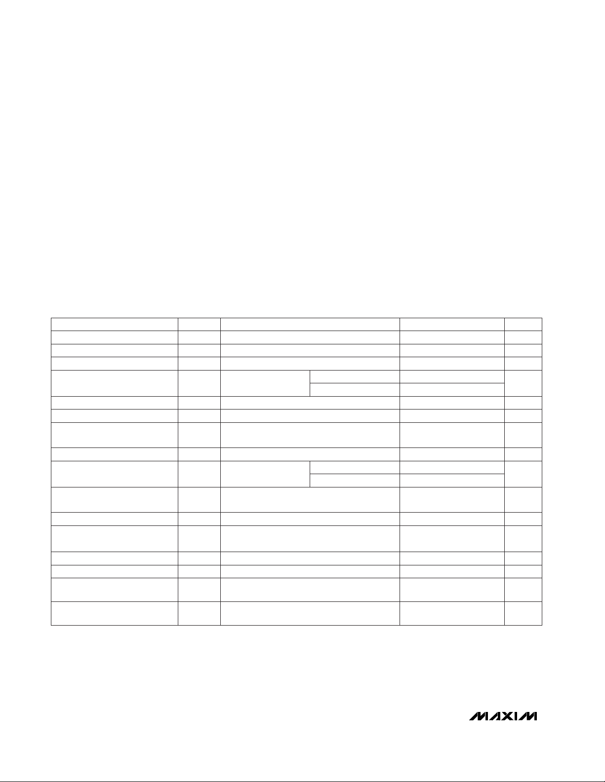
Figure 1. Required Input Signal and Output Polarity
I
MOD
= 5mA (Note 5) 300
Figure 2. Output Termination for Characterization
(Note 8) ps100Jitter Generation (peak-to-peak)
I
MOD
= 75mA
I
MOD
= 5mA
Bits80CID
Maximum Consecutive Identical
Digits at 622Mbps
I
MOD
= 75mA 10 135
DATA+
DATA-
(DATA+) -
(DATA-)
+
I
OUT
100mV MIN
800mV MAX
200mVp-p MIN
1600mVp-p MAX
I
MOD
V
CC
20Ω
1.0µF
OUT-
OUT+
BIAS
20Ω
V
CC
1.0µF
12.4Ω
15Ω
MAX3668
10Ω
OSCILLOSCOPE
50Ω
Page 4
EYE DIAGRAM
(I
MOD
= 35mA)
MAX3668 TOC02
200ps/div
PATTERN = 213 - 1 + 80 CID
I
MOD
= 35mA
622Mbps
EYE DIAGRAM
(I
MOD
= 75mA)
MAX3668 TOC03
200ps/div
PATTERN = 213 - 1 + 80 CID
I
MOD
= 75mA
622Mbps
EYE DIAGRAM
(622Mbps, 1300nm LASER
WITH 467MHz FILTER)
MAX3668 TOC01
193ps/div
2
23
- 1 PRBS
10
0.01
110100
MONITOR DIODE CURRENT
vs. APC SET RESISTOR
0.1
1
MAX3668 TOC04
R
APCSET
(kΩ)
I
MD
(mA)
1000
1
0.1 101 100
BIAS CURRENT vs.
MAXIMUM BIAS SET RESISTOR
10
100
MAX3668 TOC05
R
BIASMAX
(kΩ)
I
BIAS
(mA)
100
1
0.1 100 1000
MODULATION CURRENT
vs. MODULATION SET RESISTOR
10
MAX3688 TOC06
R
MODSET
(kΩ)
I
MOD
(mA)
101
16
17
19
18
20
21
04020 60 80
RANDOM JITTER
vs. MODULATON CURRENT
MAX3668 TOC07
I
MOD
(mA)
RANDOM JITTER (ps p-p)
INCLUDES RANDOM JITTER
DUE TO MEASUREMENT
EQUIPMENT
0
15
10
5
20
25
30
35
40
45
50
04020 60 80
PULSE-WIDTH DISTORTION
vs. MODULATION CURRENT
MAX3668 TOC08
I
MOD
(mA)
PWD (ps)
30
35
45
40
50
55
-40 10-15 35 60 85
SUPPLY CURRENT
vs. TEMPERATURE
MAX3668 TOC09
TEMPERATURE (°C)
SUPPLY CURRENT (mA)
VCC = +3.3V
VCC = +5.0V
I
BIAS
= 48mA
I
MOD
= 33mA
MAX3668
+3.3V, 622Mbps SDH/SONET
Laser Driver with Automatic Power Control
4 _______________________________________________________________________________________
Typical Operating Characteristics
(VCC= +3.3V, TA= +25°C, unless otherwise noted.)
Page 5
MAX3668
+3.3V, 622Mbps SDH/SONET
Laser Driver with Automatic Power Control
_______________________________________________________________________________________ 5
1000
0.1
1.4 1.81.6 2.2 2.6
AVAILABLE BIAS CURRENT
vs. MAXIMUM BIAS SET RESISTOR
1
10
100
MAX3668 TOC10
R
BIAS
(kΩ)
BIAS CURRENT (mA)
2.0 2.4
VCC = +3.3V
VCC = +3.3V, + 5V
CLOSED-LOOP OPERATION
VCC = +5V
0
5
15
10
20
25
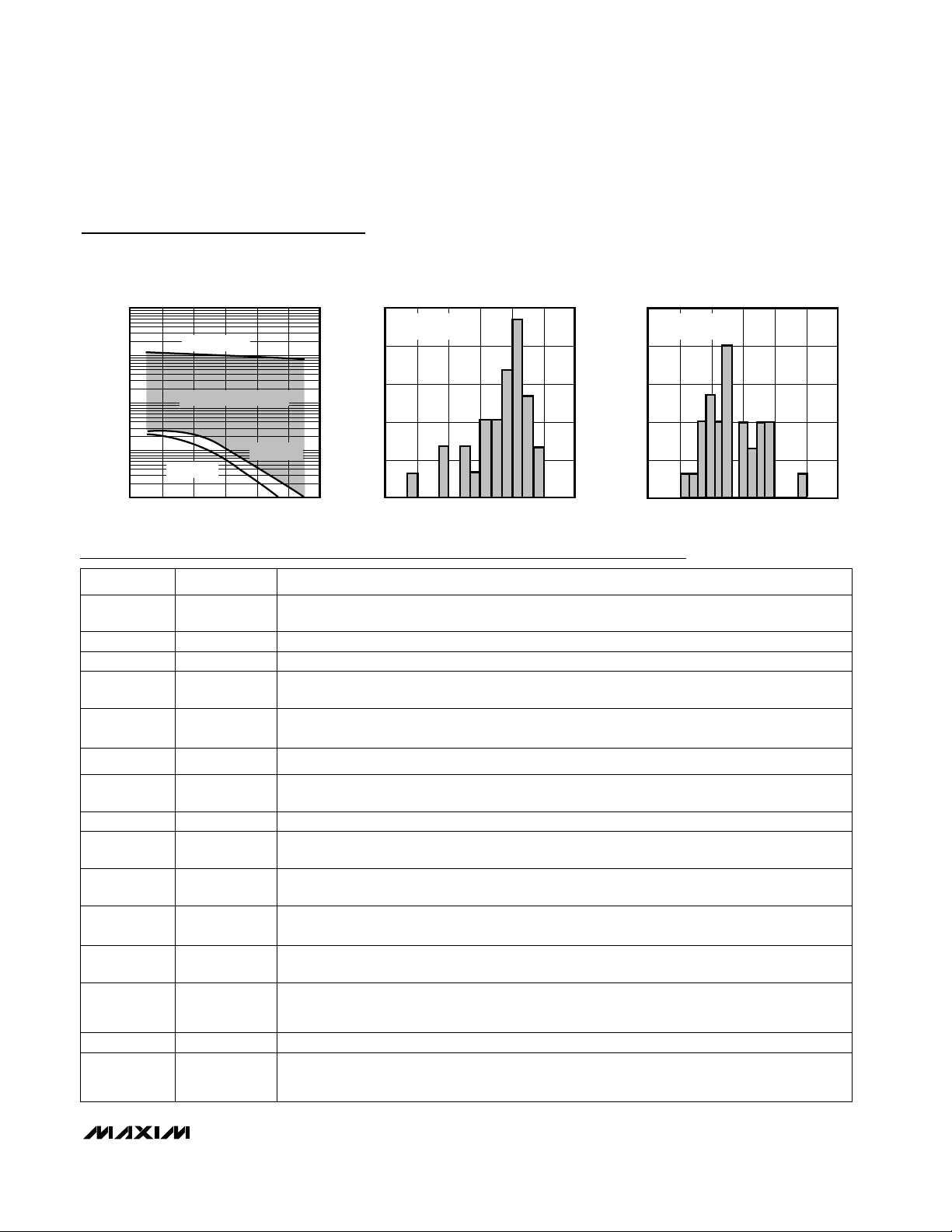
-25 15565 245 335 425 515
DISTRIBUTION OF MODULATION CURRENT
STABILITY (WORST CASE)
MAX3668-11
MODULATION DIODE CURRENT STABILITY (ppm/°C)
PERCENT OF UNITS (%)
TA = -40°C TO +85°C
I
MOD
= 5mA
0
5
15
10
20
25
-52-88 20 92 160
DISTRIBUTION OF MONITOR DIODE CURRENT
STABILITY (WORST CASE)
MAX3668-12
MONITOR DIODE CURRENT STABILITY (ppm/°C)
PERCENT OF UNITS (%)
TA = -40°C TO +85°C
I
MD
= 18µA
Typical Operating Characteristics (continued)
(VCC= +3.3V, TA= +25°C, unless otherwise noted.)
Pin Description
NAME FUNCTION
1, 2, 6, 15,
17, 20, 24
V
CC
Positive Supply Voltage
29 APCSET
APC Set Resistor. A resistor connected from this pad to ground sets the desired average optical power. The resulting current is equal to the desired DC monitor diode current. Connect a
100kΩ resistor from this pad to ground if APC is not used.
PIN
3 DATA+ Positive PECL Data Input
4 DATA- Negative PECL Data Input
32 BIASMAX
Maximum Bias Set Resistor. A resistor from this pad to ground sets the maximum laser bias
current. The APC function can subtract from this maximum value but cannot add to it. This
resistor controls the bias-current level when the APC loop is not used.
31 MODSET Modulation Set Resistor. A resistor from this pad to ground sets the laser modulation current.
5, 7, 8, 10,
14, 21, 22, 30
GND Ground
12, 13, 26,
27, 28
N.C. No Connection. Leave unconnected.
11
FAIL
TTL Output. Indicates APC failure when low. Internally pulled high through a 6kΩ resistor.
9 ENABLE
TTL/CMOS Enable Input. High for normal operation, low to disable laser bias and modulation
currents. Internally pulled high.
16 BIAS Laser Bias Current Output. Isolate from laser with a ferrite bead.
19 OUT-
Negative Modulation Current Output. I
MOD
flows into this pad when the input signal is low.
Connect this pad to V
CC
through a 6.3Ω resistor.
18 OUT+
Positive Modulation Current Output. I
MOD
flows into this pad when the input signal is high.
Connect this pad to AC coupling network.
23 MD
Monitor Photodiode Connection. Connect this pad to the monitor photodiode anode. A capacitor to ground is required to filter high-speed AC monitor photocurrent.
25 CAPC
APC Compensation Capacitor. A 0.1µF capacitor connected from this pad to ground controls
the dominant pole of the automatic power control (APC) feedback loop.
Page 6
MAX3668
+3.3V, 622Mbps SDH/SONET
Laser Driver with Automatic Power Control
6 _______________________________________________________________________________________
MAX3668
DATA+
OUT+
OUT-
DATA-
100k
ENABLE
I
MD
R
APCSET
R
BIASMAX
R
MODSET
APCSET
CAPC
C
APC
BIASMAX
MD
MODSET
FAIL
BIAS
I
BIAS
165X
V
CC
FAILURE
DETECTOR
40X
5X
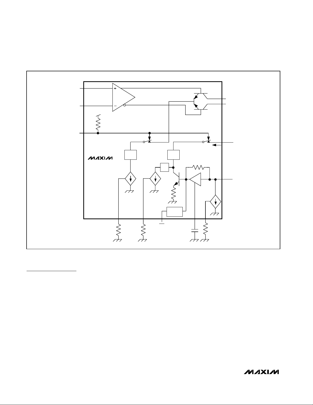
Figure 3. Functional Diagram
Detailed Description
The MAX3668 laser driver consists of two main parts: a
high-speed modulation driver and a laser-biasing block
with Automatic Power Control (APC). The circuit is optimized for low-voltage (+3.3V) operation.
The output stage is composed of a high-speed differential
pair and a programmable modulation current source.
Since the modulation output drives a maximum current
of 75mA into the laser with a 230ps edge speed, large
transient voltage spikes can be generated due to the
parasitic inductance. These transients and the laser forward voltage leave insufficient headroom for the proper
operation of the laser driver if the modulation output is
DC-coupled to the laser diode. To solve this problem,
the MAX3668’s modulation output is designed to be
AC-coupled to the cathode of a laser diode. A simplified functional diagram is shown in Figure 3.
The MAX3668 modulation output is optimized for driving a 20Ω 10Ω load; the minimum required voltage at
OUT+ is 2.0V. Modulation current swings of 75mA are
possible. To interface with the laser diode, a damping
resistor (R
D
) is required for impedance matching. An
RC shunt network may be used to compensate for the
laser-diode parasitic inductance, thereby improving the
optical output aberrations and duty-cycle distortion.
At a 622Mbps data rate, any capacitive load at the cathode of a laser diode degrades the optical output performance. Since the BIAS output is directly connected to the
laser cathode, minimize the parasitic capacitance associated with this pin by using an inductor to isolate the BIAS
pin from the laser cathode.
Page 7
Automatic Power Control
To maintain constant average optical power, the
MAX3668 incorporates an APC loop to compensate for
the changes in laser threshold current over temperature
and lifetime. A back-facet photodiode mounted in the
laser package is used to convert the optical power into a
photocurrent. The APC loop adjusts the laser bias current so the monitor current is matched to a reference current set by R
APCSET
. The time constant of the APC loop
is determined by an external capacitor (C
APC
). To eliminate the pattern-dependent jitter associated with the
APC loop-time constant and to guarantee loop stability,
the recommended value for C
APC
is 0.1µF.
When the APC loop is functioning, the maximum allowable
bias current is set by an external resistor, R
BIASMAX
. An
APC failure flag (FAIL) is set low when the bias current can
no longer be adjusted to achieve the desired average
optical power.
APC closed-loop operation requires the user to set three
currents with external resistors connected between
ground and BIASMAX, MODSET, and APCSET. Detailed
guidelines for these resistor settings are described in
the Design Procedure section.
Open-Loop Operation
If necessary, the MAX3668 is fully operational without
APC. In this case, the laser current is directly set by two
external resistors connected from ground to BIASMAX
and MODSET. Connect a 100kΩ resistor from APCSET
to ground and leave MD open for open-loop operation.
Enable Control
The MAX3668 incorporates a laser driver enable function. When ENABLE is low, both the bias and modulation
currents are off. The typical laser enable time is 250ns.
APC Failure Monitor
The MAX3668 provides an APC failure monitor
(TTL/CMOS) to indicate an APC loop tracking failure. FAIL
is set low when the APC loop can no longer adjust the bias
current to maintain the desired monitor current. This output
is internally pulled up to VCCthrough a 6kΩ resistor.
Short-Circuit Protection
The MAX3668 provides short-circuit protection for the
modulation, bias, and monitor current sources. If either
BIASMAX, MODSET, or APCSET is shorted to ground,
the bias and modulation outputs will be turned off.
Design Procedure
When designing a laser transmitter, the optical output is
usually expressed in terms of average power and extinction ratio. Table 1 gives the relationships that are helpful
in converting between the optical average power and the
modulation current. These relationships are valid if the
average duty cycle of the optical waveform is 50%.
Programming the Modulation Current
In addition to being a function of R
MODSET
, the modula-
tion current delivered to the laser (I
MODL
) also depends
on the values of the series damping resistor (RD), the
shunt compensation resistance (R
FILT
), and the laser
diode’s resistance (see Typical Operating Circuit).
The modulation current (assuming C
FILT
<<CD) into the
laser diode can be represented by the following:
Assuming R
D
= 5Ω and r
LASER
= 5Ω, this equation is
simplified to:
I
MODL
= I
MOD
(0.67)
For R
D
= 5.0Ω and a laser resistance of approximately
5Ω, refer to the Modulation Current vs. Modulation Set
Resistor graph in the Typical Operating Characteristics
and select the value of R
MODSET
that corresponds to
the required current at +25°C.
Programming the Bias Current
When using the MAX3668 in open-loop operation, the
bias current is determined by the R
BIASMAX
resistor. To
select this resistor, determine the required bias current
at +25°C. Refer to the Bias Current vs. Maximum Bias
Set Resistor graph in the Typical Operating Character-
istics and select the value of R
BIASMAX
that corresponds to the required current at +25°C.
When using the MAX3668 in closed-loop operation, the
R
BIASMAX
resistor sets the maximum bias current available to the laser diode over temperature and life. The
APC loop can subtract from this maximum value but
cannot add to it. Refer to the Bias Current vs. Maximum
Bias Set Resistor graph in the Typical Operating
Characteristics and select the value of R
BIASMAX
that
corresponds to the end-of-life bias current at +85°C.
I = I
2
2 + R+ r
MODL MOD
D LASER
00Ω
Ω
()
MAX3668
+3.3V, 622Mbps SDH/SONET
Laser Driver with Automatic Power Control
_______________________________________________________________________________________ 7
Table 1. Optical Power Definition
I
MOD
= Pp-p / η
I
MOD
Modulation Current
η = Pp-p / I
MOD
η
Laser Slope Efficiency
Pp-p = 2P
AVE(re
- 1) / (re+ 1)Pp-pOptical Amplitude
P0= 2P
AVE
/ (re+ 1)P
0
Optical Power Low
P1= 2P
AVE
· re/ (re+ 1)P
1
Optical Power High
re= P1/ P
0
r
e
Extinction Ratio
P
AVE
= (P0+ P1) / 2P
AVE
Average Power
RELATIONSYMBOLPARAMETER
Page 8
MAX3668
+3.3V, 622Mbps SDH/SONET
Laser Driver with Automatic Power Control
8 _______________________________________________________________________________________
Programming the APC Loop
When the MAX3668’s APC feature is used, program the
average optical power by adjusting the APCSET resistor. To select this resistor, determine the desired monitor current to be maintained over temperature and life.
Refer to the Monitor Diode Current vs. APC Set Resistor
graph in the Typical Operating Characteristics and
select the value of R
APCSET
that corresponds to the
required current.
Interfacing with the Laser Diode
To minimize optical output aberrations due to the laser
parasitic inductance, an RC shunt network may be
used (see Typical Operating Circuit). If RLrepresents
the laser diode resistance, the recommended total
resistance for RD+ RLis 10Ω. Starting values for coaxi-
al lasers are R
FILT
= 20Ω and C
FILT
= 5pF. R
FILT
and
C
FILT
should be experimentally adjusted to optimize
the output waveform. A bypass capacitor should also
be placed as close to the laser anode as possible for
best performance.
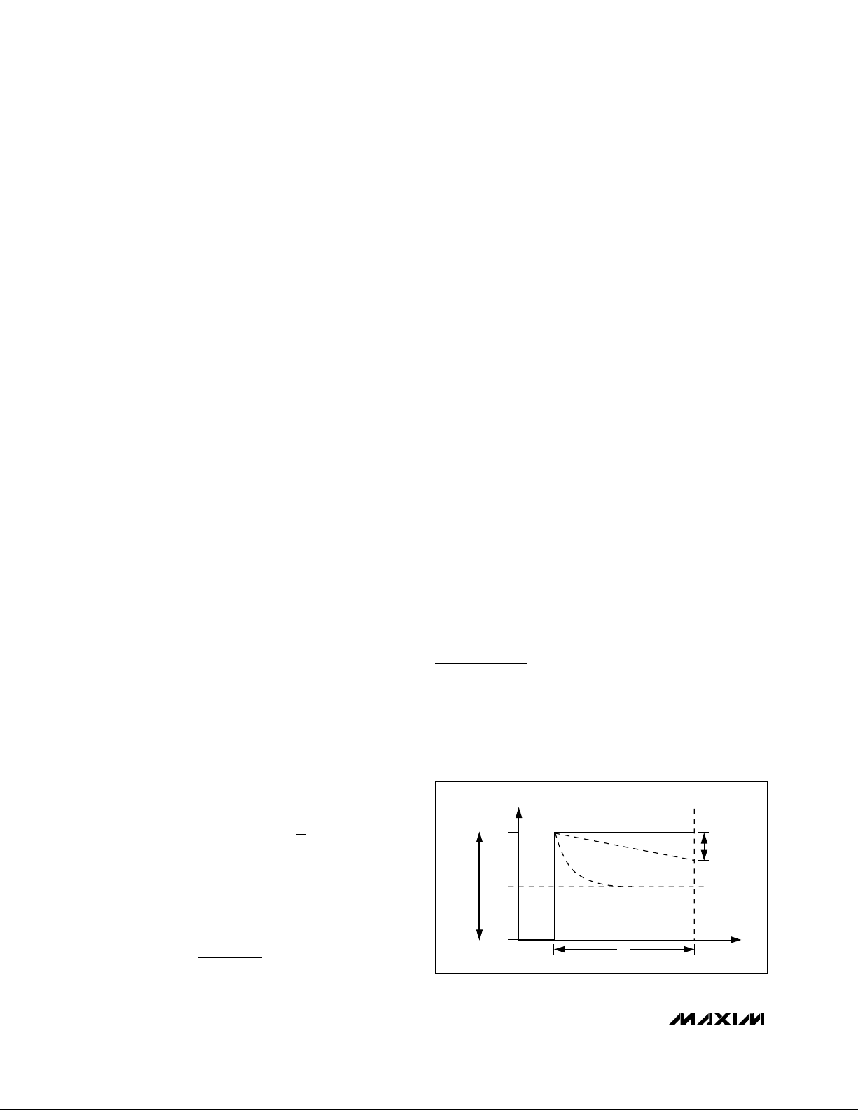
Pattern-Dependent Jitter (PDJ)
When transmitting NRZ data with long strings of consecutive identical digits (CID), LF droop can contribute to
pattern-dependent jitter. To minimize this pattern-dependent jitter, two external components must be properly
chosen: capacitor C
APC
, which dominates the APC loop
time constant; and AC-coupling capacitor CD.
To filter out noise effects and guarantee loop stability,
the recommended value for C
APC
is 0.1µF. This results
in an APC loop bandwidth of 20kHz. Consequently, the
pattern-dependent jitter associated with an APC loop
time constant can be ignored.
The time constant associated with the DC blocking
capacitor on I
MOD
will have an effect on PDJ. It is
important that this time constant produce minimum
droop for long consecutive bit streams.
Referring to Figure 4, the droop resulting from long time
periods without transitions can be represented by the
following equation:
AC coupling of I
MOD
results in a discharge level for τ
that is equal to P
AVG
. An overall droop of 6% relative to
P
p-p
equates to a 12% droop relative to P
AVG
. To
ensure a droop of less than 12% (6% relative to P
p-p
),
this equation can be solved for τ as follows:
If t
1
equals 80 consecutive unit intervals without a transition, the time constant associated with the DC blocking capacitor needs to be longer than:
τAC≥ RACCD= 7.8 (80 bits) (1.6ns/bit) = 1.0µs
R
FILT
can be ignored for C
FILT
<< CD, therefore the
estimated value of RACis:
RAC= 20Ω (RD+ r
LASER
)
Assuming RD= 5Ω, and r
LASER
= 5Ω:
RAC= 6.7Ω
with CD= 1.0µF, τAC= 6.7µs.
Input Termination Requirement
The MAX3668 data inputs are PECL-compatible.
However, it is not necessary to drive the MAX3668 with
a standard PECL signal. As long as the specified common-mode voltage and differential voltage swings are
met, the MAX3668 will operate properly.
Calculate Power Consumption
The total power dissipation of the MAX3668 can be estimated by the following:
P = V
CC
× I
CC
+ (VCC- V
f
) × I
BIAS
+ I
MOD(VCC
- 20Ω × I
MOD
/ 2)
where I
BIAS
is the maximum bias current set by R
BIAS-
MAX
, I
MOD
is the modulation current, and Vfis the typi-
cal laser forward voltage.
Applications Information
The following is an example of how to set up the
MAX3668.
Select Laser
A communication-grade laser should be selected for
622Mbps applications. Assume the laser output average power is P
AVE
= 0dBm, the minimum extinction
(1 - 0.12)
-t
τ = = 7.8t
ln
(100% - DROOP) = e
-t
τ
DROOP
t
P
AVG
P
p-p
τ = ∞
τ << τ
AC
τ
AC
t
1
Figure 4. Droop
Page 9

ratio is re= 6.6 (8.2dB), the operating temperature is
-40°C to +85°C, and the laser diode has the following
characteristics:
Wavelength: λ = 1.3µm
Threshold Current: ΙTH= 22mA at +25°C
Threshold Temperature
Coefficient: β
TH
= 1.3%/°C
Laser to Monitor Transfer: ρ
MON
= 0.2A/W
Laser Slope Efficiency: η = 0.05mW/mA
at +25°C
Determine R
APCSET
The desired monitor diode current is estimated by
IMD= P
AVE
×
ρ
MON
= 200µA. The Monitor Diode Current
vs. APC Set Resistor graph in the Typical Operating
Characteristics shows that R
APCSET
should be 6kΩ.
Determine R
MODSET
To achieve a minimum extinction ratio (re) of 6.6 over
temperature and lifetime, calculate the required extinction ratio at +25°C. Assuming re= 20, the peak-to-peak
optical power P
p-p
= 1.81mW according to Table 1. The
required modulation current is 1.81(mW) / 0.05(mW/mA)
= 36.2mA. The Modulation Current vs. Modulation Set
Resistor graph in the (see Typical Operating Characteri-
stics) shows that R
MODSET
should be 5kΩ.
Determine R
BIASMAX
Calculate the maximum threshold current (I
TH(MAX)
) at
TA= +85°C and end of life. Assuming I
TH(MAX)
=
50mA, the maximum bias current should be:
I
BIAS
= I
TH(MAX)
+ I
MOD
/ 2
In this example, I
BIAS
= 68.1mA. The Bias Current vs.
Maximum Bias Set Resistor graph in the Typical
Operating Characteristics shows that R
BIASMAX
should
be 3kΩ.
Modulation Current More than 50mA
To drive modulation currents greater than 50mA at
3.3V, external pull-up inductors (Figure 5) should be
used to DC-bias the modulation output at VCC. Such a
configuration isolates the laser forward voltage from the
output circuitry and allows the output at OUT+ to swing
above and below the supply voltage V
CC
.
At +5V power supply, the headroom voltage for the
MAX3668 is significantly improved. In this case, it is
possible to achieve a modulation current of more than
50mA (using resistor pull-ups as shown in the Typical
Operating Circuit). The MAX3668 can also be DC-coupled
to a laser diode when operating at +5V supply; the voltage at OUT+ should be ≥2.0V for proper operation.
Wire Bonding Die
For high current density and reliable operation, the
MAX3668 uses gold metalization. Make connections to
the die with gold wire only, using ball-bonding techniques. Wedge bonding is not recommended. Die-pad
size is 4 mils (100µm) square, and die thickness is 12
mils (300µm) mils.
Layout Considerations
To minimize inductance, keep the connections between
the MAX3668 output pins and LD as close as possible.
Optimize the laser diode performance by placing a
bypass capacitor as close as possible to the laser
anode. Use good high-frequency layout techniques
and multilayer boards with uninterrupted ground planes
to minimize EMI and crosstalk.
Laser Safety and IEC 825
Using the MAX3668 laser driver alone does not ensure
that a transmitter design is compliant with IEC 825. The
entire transmitter circuit and component selections must
be considered. Customers must determine the level of
fault tolerance required by their application, recognizing
that Maxim products are not designed or authorized for
use as components in systems intended for surgical
implant into the body, for applications intended to support or sustain life, or for any other application where the
failure of a Maxim product could create a situation
where personal injury or death may occur.
MAX3668
+3.3V, 622Mbps SDH/SONET
Laser Driver with Automatic Power Control
_______________________________________________________________________________________ 9
LD
C
D
R
FILT
C
FILT
1000pF
1.0µF5Ω
10Ω
R
D
V
CC
FERRITE
BEADS
FERRITE BEAD
MD
BIAS
OUT+
OUT-
MAX3668
Figure 5. Output Termination for Maximum Modulation Current
Page 10

MAX3668
+3.3V, 622Mbps SDH/SONET
Laser Driver with Automatic Power Control
10 ______________________________________________________________________________________
V
CC
N.C.
V
CC
V
CC
V
CC
V
CC
0.083"
(2.10mm)
0.070"
(1.78mm)
V
CC
BIASMAX
MODSET
GND
GND
V
CC
CAPC
N.C.
GND
N.C.
APCSET
N.C.
GND
GND
ENABLE
GND
GND
V
CC
BIAS
GND
N.C.
N.C.
GND
N.C.
V
CC
FAIL
GND
GND
MD
GND
N.C.
OUT-
N.C.
GND
DATA-
DATA+
V
CC
V
CC
GND
OUT+
GND
N.C.
Chip Topography
MAX3668
TQFP
TOP VIEW
32 28
293031
25
26
27
MODSET
GND
APCSET
N.C.
BIASMAX
N.C.
N.C.
CAPC
10
13
15
14
1611 12
9
ENABLE
FAIL
GND
N.C.
N.C.
V
CC
GND
BIAS
17
18
19
20
21
22
23
MD
24 V
CC
GND
GND
V
CC
OUT-
OUT+
V
CC
2
3
4
5
6
7
8GND
GND
V
CC
GND
DATA-
DATA+
V
CC
1V
CC
Pin Configuration
Page 11
MAX3668
+3.3V, 622Mbps SDH/SONET
Laser Driver with Automatic Power Control
______________________________________________________________________________________ 11
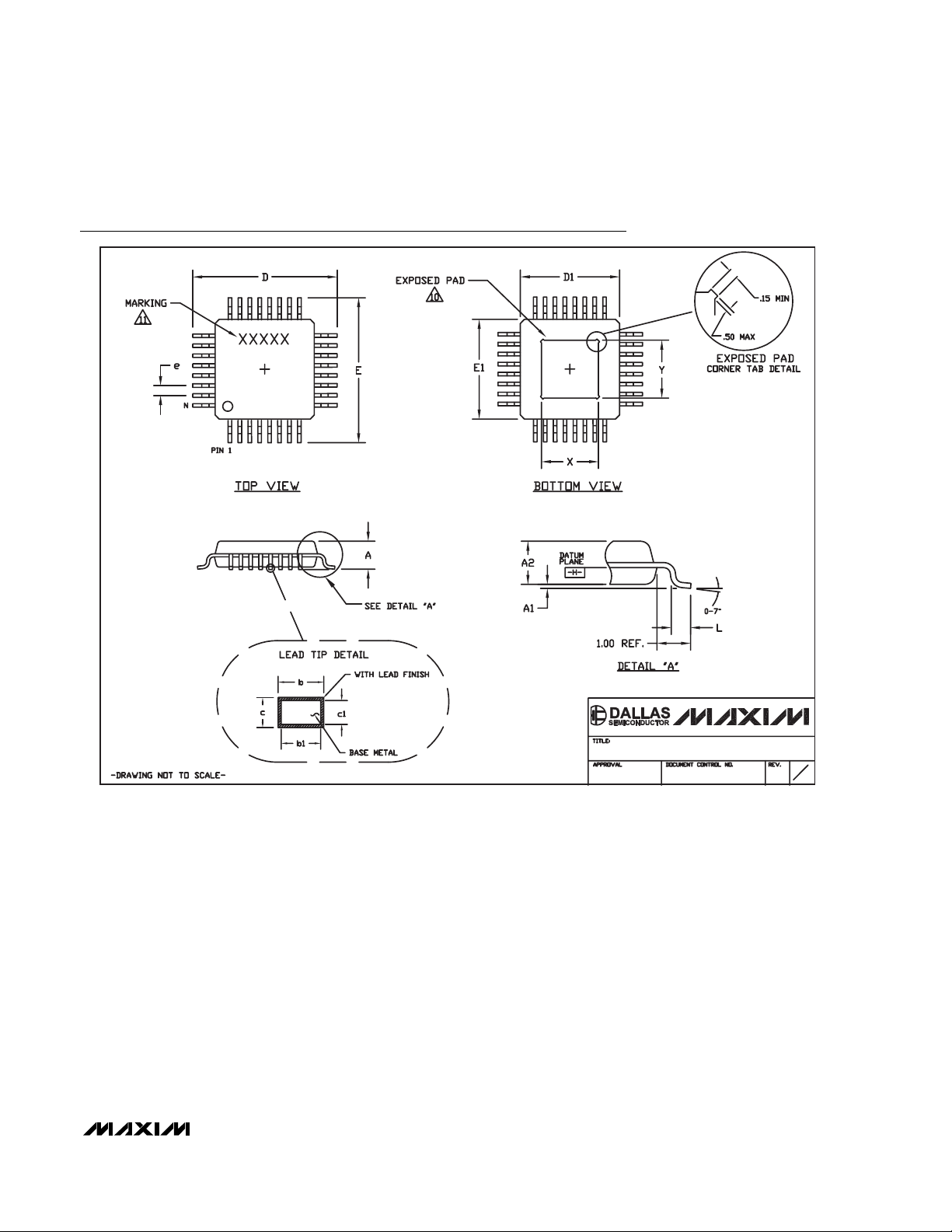
32L,TQFP.EPS
F
1
2
21-0079
PACKAGE OUTLINE,
32L TQFP, 5x5x1.0mm, EP OPTION
Package Information
(Package information continues on next page.)
Page 12

MAX3668
+3.3V, 622Mbps SDH/SONET
Laser Driver with Automatic Power Control
Maxim makes no warranty, representation or guarantee regarding the suitability of its products for any particular purpose, nor does Maxim assume any liability arising out of the application or use of any product or circuit and specifically disclaims any and all liability, including without limitation consequential or
incidental damages. “Typical” parameters can and do vary in different applications. All operating parameters, including “typicals” must be validated for
each customer application by customer’s technical experts. Maxim products are not designed, intended or authorized for use as components in systems
intended for surgical implant into the body, or other applications intended to support or sustain life, or for any other application in which the failure of the
Maxim product could create a situation where personal injury or death may occur.
12 ____________________Maxim Integrated Products, 120 San Gabriel Drive, Sunnyvale, CA 94086 408-737-7600
© 2005 Maxim Integrated Products Printed USA is a registered trademark of Maxim Integrated Products, Inc.
Package Information (continued)
F
2
2
21-0079
PACKAGE OUTLINE,
32L TQFP, 5x5x1.0mm, EP OPTION
 Loading...