

________________General Description
The MAX3667 is a complete, +3.3V laser driver with
automatic power control (APC), designed for SDH/
SONET applications up to 622Mbps. It accepts differential PECL inputs, provides single-ended bias and
modulation currents, and operates over a -40°C to
+85°C temperature range.
A temperature-stabilized reference voltage simplifies
laser current programming. It allows external programming of the modulation current between 5mAp-p and
60mAp-p, and of the bias current between 5mA and
90mA.
The APC function, which incorporates a monitor photodiode, an external resistor, and two external capacitors,
maintains constant laser output power. Two current
monitors provide high-speed signals that are directly
proportional to the bias and modulation currents.
Additional features include disable/enable control and
a slow-start feature with a minimum turn-on time of
50ns. The MAX3667 is available in die form and in a
32-pin TQFP package.
________________________Applications
622Mbps SDH/SONET Access Nodes
Laser Driver Transmitters
Section Repeaters
____________________________Features
♦ Single +3.3V or +5.0V Operation
♦ Automatic Average Power Control
♦ Bias Current and Modulation Current Monitor
Outputs
♦ TTL-Compatible Disable Input
♦ Temperature-Compensated Reference
♦ PECL-Compatible Data Inputs
MAX3667
+3.3V, 622Mbps SDH/SONET Laser Driver
with Automatic Power Control
________________________________________________________________
Maxim Integrated Products
1
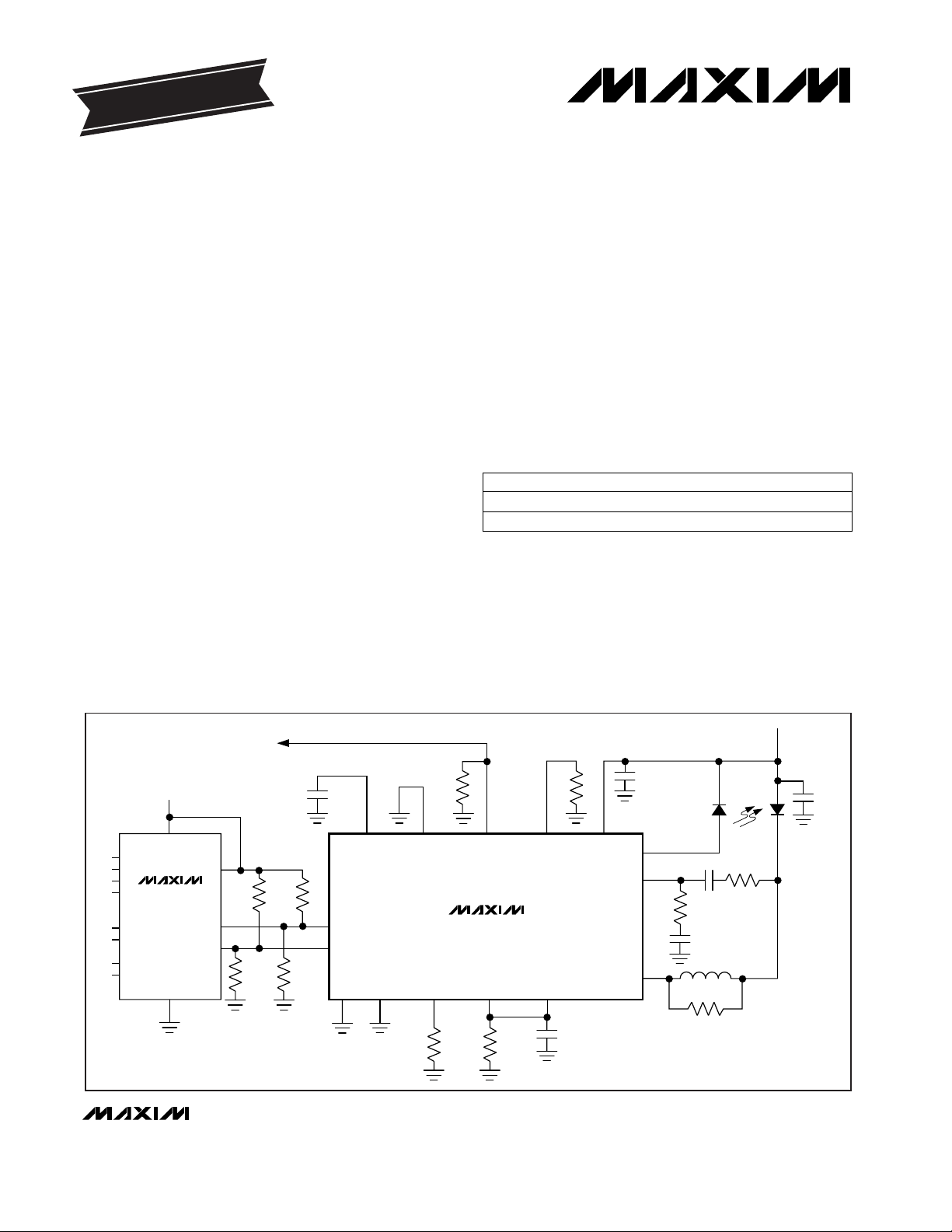
MAX3667
MAX3691
130Ω 130Ω
50Ω
82Ω 82Ω
PECL
1µF
DISABLE
COMP
C
COMP
BIASMON MODMON APCSET
MD
MONITOR
DIODE
+3.3V
LASER
DIODE
IMOD
R
FILT
22Ω
R
DAMP
4.7Ω
100Ω
470nH
4:1
SERIALIZER
WITH
CLOCK GEN
1µF
0.01µF
0.1µF
0.1µF
IBIAS
MODSETGND
IN+
IN-
BIASSET APC
C
APC
1nF
V
CC
+3.3V
____________________________________________________Typical Operating Circuit
19-1311; Rev 1; 3/98
PART
MAX3667ECJ
MAX3667E/D -40°C to +85°C
-40°C to +85°C
TEMP. RANGE PIN-PACKAGE
32 TQFP
Dice*
EVALUATION KIT
AVAILABLE
_______________Ordering Information
Pin Configuration appears at end of data sheet.
*
Dice are designed to operate from -40°C to +85°C but are
tested and guaranteed only at T
j
= +25°C.
For free samples & the latest literature: http://www.maxim-ic.com, or phone 1-800-998-8800.
For small orders, phone 408-737-7600 ext. 3468.
MAX3667
+3.3V, 622Mbps SDH/SONET Laser Driver
with Automatic Power Control
2 _______________________________________________________________________________________
ABSOLUTE MAXIMUM RATINGS
DC ELECTRICAL CHARACTERISTICS
(VCC= +3.3V ±5%, TA= -40°C to +85°C, unless otherwise noted.) (Notes 1, 2)
Stresses beyond those listed under “Absolute Maximum Ratings” may cause permanent damage to the device. These are stress ratings only, and functional
operation of the device at these or any other conditions beyond those indicated in the operational sections of the specifications is not implied. Exposure to
absolute maximum rating conditions for extended periods may affect device reliability.
Supply Voltage, VCC..............................................-0.5V to +7.0V
Current into IBIAS..............................................-50mA to 350mA
Current into IMOD .............................................-50mA to 200mA
Current into MD ..................................................................±7mA
Voltage at APC, MODMON,
BIASMON, COMP....................................-0.5V to (V
CC
+ 0.5V)
Voltage at IN+, IN-, DISABLE, MODSET,
BISASSET, APCSET, PULLUP..................-0.5V to (V
CC
+ 0.5V)
Continuous Power Dissipation (TA= +85°C)
TQFP (derate 11.1mW/°C above +85°C)......................721mW
Operating Temperature Range ...........................-40°C to +85°C
Operating Junction Temperature Range (die) ..-55°C to +175°C
Processing Temperature (die).........................................+400°C
Storage Temperature Range.............................-65°C to +160°C
Lead Temperature (soldering, 10sec).............................+300°C
VIN= 1.82V
VIN= 2.14V
Disable = high
(Note 5)
R
APCSET
= 33.2kΩ
Closed loop (Note 4)
R
APCSET
= 2kΩ
R
MODSET
= 33.2kΩ (Note 10)
R
MODSET
= 2kΩ (Note 10)
R
MODSET
= 33.2kΩ, open loop (Note 8)
R
MODSET
= 2kΩ, open loop (Note 8)
R
BIASSET
= 33.2kΩ
R
BIASSET
= 2kΩ
R
BIASSET
= 2kΩ, closed loop (Notes 4, 9)
R
BIASSET
= 33.2kΩ, open loop (Note 8)
Disable = high
Disable = high or low
R
MODSET
= 2kΩ (Note 10)
R
BIASSET
= 2kΩ, open loop (Note 8)
R
BIASSET
= 2kΩ
CONDITIONS
V2.0V
DIH
TTL Disable High Voltage
µA2 10I
IH
PECL Input Low Current
µA4.5 10I
IH
PECL Input High Current
V1.82V
IL
PECL Input Low Voltage
V2.14V
IH
PECL Input High Voltage
164 205 250
A/A
135 170 205
A
I
I
APCSET
to IBIAS Gain
152 190 230
A/A
152 190 230
A
I
I
MODSET
to I
QMOD
Gain
128 160 195
A/A
145 170 200
A
I
I
BIASSET
to IBIAS Gain
A/A26 33 40A
I
MODMON to I
QMOD
Gain
A/A30 38 46A
I
BIASMON to IBIAS Gain
µA5 250I
BIAS
Bias Off Current
mA5 90I
BIAS
mA112 133I
CC
Supply Current (Note 3)
Bias Current Range
1100
ppm/°C
1100
Modulation Current Stability
480
1000
µA20 250I
BIAS
Modulation Off Current
Ω26 31 35R
PULL-UP
Internal Pull-Up Resistor
(Note 6)
V0.91 1.01 1.11V
REF
Reference Voltage (Note 7)
ppm/°C
500
Bias Current Stability
UNITSMIN TYP MAXSYMBOLPARAMETER
µA4I
DIL
TTL Disable Low Current
µA1I
DIH
TTL Disable High Current
V0.8V
DIL
TTL Disable Low Voltage
MAX3667
+3.3V, 622Mbps SDH/SONET Laser Driver
with Automatic Power Control
_______________________________________________________________________________________ 3
Note 1: Dice are tested at TA= +27°C.
Note 2: Minimum voltage at IBIAS = V
CC
- 1.6V.
Note 3: The sum of the currents flowing into V
CC
and PULLUP with R
BIASSET
= R
MODSET
= R
APCSET
= 2kΩ, IN+ = 1.82V,
IN- = 2.14V.
Note 4: APC is connected to BIASSET for closed-loop operation.
Note 5: Bias current range is guaranteed by the I
BIASSET
to IBIAS gain test.
Note 6: R
PULL-UP
is connected between IMOD and PULLUP.
Note 7: V
REF
is the voltage on BIASSET, MODSET, or APCSET with R
BIASSET
= R
MODSET
= R
APCSET
= 2kΩ.
Note 8: APC is disconnected from BIASSET for open-loop operation.
Note 9: Bias current stability is guaranteed by design and characterization.
Note 10: I
QMOD
is the current flowing into the collector of Q
MOD
(Figure 1).
Note 11: AC parameters are guaranteed by design and characterization.
Note 12: Modulation current range is guaranteed by the I
MODSET
to I
QMOD
gain test.
Note 13: Input signal is a 155Mbps 1-0 pattern. PWD = [(width of wider pulse) - (width of narrower pulse)] / 2.
Disable = high
Disable = high
Closed loop (Note 4)
R
APCSET
= 33.2kΩ
R
APCSET
= 2kΩ
VIN= 3.52V
VIN= 3.84V
R
MODSET
= 33.2kΩ (Note 10)
R
MODSET
= 2kΩ (Note 10)
R
BIASSET
= 2kΩ
R
MODSET
= 2kΩ (Note 10)
R
BIASSET
= 2kΩ
R
BIASSET
= 33.2kΩ
CONDITIONS
µA8I
IH
PECL Input Low Current
µA9I
IH
PECL Input High Current
V3.52V
IL
PECL Input Low Voltage
V3.84V
IH
PECL Input High Voltage
µA32 250Modulation Off Current
µA2 250
mA134 160I
CC
Supply Current (Note 3)
Bias Off Current
145 182 220
A/A
132 166 200
A
I
I
APCSET
to IBIAS Gain
188 230 285
A/A
168 240 315
A
I
I
MODSET
to I
QMOD
Gain
A/A38A
I
BIASMON to IBIAS Gain
A/A26 33 40A
I
MODMON to I
QMOD
Gain
A/A
145 180 220
A
I
I
BIASSET
to IBIAS Gain
143 180 215
UNITSMIN TYP MAXSYMBOLPARAMETER
VCC= 5.0V ±5%, 20% to 80%
VCC= 3.3V ±5%, 20% to 80%
R
FILT
= 22Ω, R
DAMP
= 0Ω (Note 12)
VCC= 3.3V ±5%, 20% to 80%
VCC= 5.0V ±5%, 20% to 80%
R
FILT
= 22Ω, R
DAMP
= 0Ω (Note 13)
CONDITIONS
205 400
ps
270 450
t
r
mA5 60I
MOD
Modulation Current Range
Output Rise Time
ps
425 650
t
f
Output Fall Time
315 600
%±10Output Aberrations
ps70PWDPulse-Width Distortion
UNITSMIN TYP MAXSYMBOLPARAMETER
DC ELECTRICAL CHARACTERISTICS
(VCC= +5.0V ±5%, TA= -40°C to +85°C, unless otherwise noted.) (Notes 1, 2)
AC ELECTRICAL CHARACTERISTICS
(VCC= +3.3V ±5%, TA= -40°C to +85°C, R
LOAD
= 10Ω, unless otherwise noted.) (Notes 2, 11)
MAX3667
+3.3V, 622Mbps SDH/SONET Laser Driver
with Automatic Power Control
4 _______________________________________________________________________________________
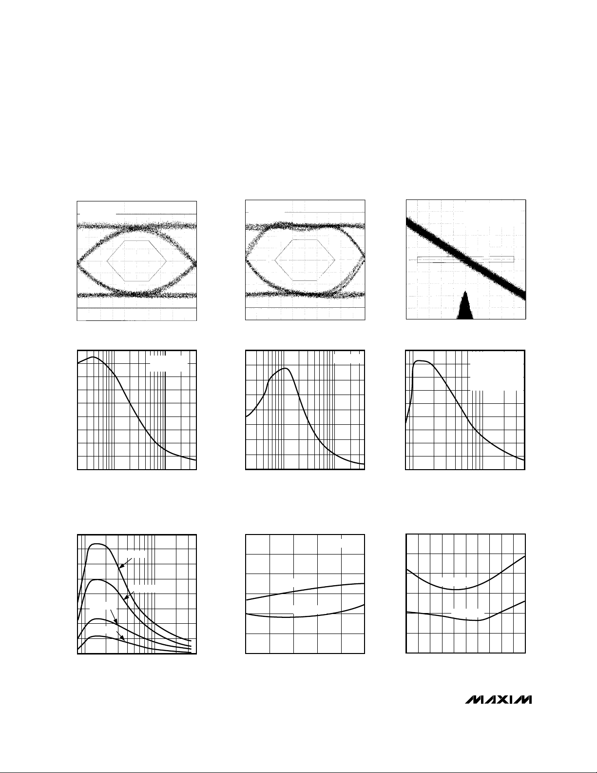
__________________________________________Typical Operating Characteristics
(TA = +25°C, VCC= +3.3V, unless otherwise noted.)
161ps/div
52mV/
div
EYE DIAGRAM
(622Mbps, 1300nm LASER,
470MHz FILTER)
MAX3667-01
2
23
- 1PRBS
I
MOD
= 15mA
DIFF. INPUT = 640mVp-p
161ps/div
20mV/
div
EYE DIAGRAM
(622Mbps, 10Ω LOAD)
MAX3667-02
2
23
- 1PRBS
I
MOD
= 15mA
DIFF. INPUT = 1.7Vp-p
10ps/div
5mV/
div
OUTPUT JITTER
(622Mbps, 10Ω LOAD)
MAX3667-03
I
MOD
= 20mA
DIFF. INPUT = 1.7Vp-p
∆RMS = 3.2ps
180
160
140
0
200
1k
40k
I
BIAS
vs. R
BIASSET
60
40
20
120
100
80
MAX3667-04
R
BIASSET
(Ω)
I
BIAS
(mA)
10k
V
IBIAS
= 1.7V
10Ω LOAD
0
30
20
10
60
50
40
70
80
1k 10k 40k
I
BIAS
vs. R
APCSET
(VARYING MONITOR-TO-LASER
CURRENT GAIN)
MAX3667-07
R
APCSET
(Ω)
I
BIAS
(mA)
GAIN = 90
GAIN = 60
GAIN = 30
GAIN = 15
160
140
120
0
I
QMOD
vs. R
MODSET
60
40
20
100
80
MAX3667-05
R
MODSET
(Ω)
I
QMOD
(mA)
200
1k
40k10k
10Ω LOAD
0
0.4
0.3
0.2
0.1
0.7
0.6
0.5
0.8
0.9
1k 10k 40k
IMD vs. R
APCSET
R
APCSET
(Ω)
I
MD
(mA)
APC LOOP CLOSED
R
BIASSET
= 2kΩ
R
MODSET
= 2kΩ
MONITOR-TO-LASER
CURRENT GAIN = 82
MAX3667-06
0
20
60
40
100
80
120
-40 -15 10 35 60 85
PULSE-WIDTH DISTORTION
vs. TEMPERATURE
MAX3667toc08
PULSE-WIDTH DISTORTION (ps)
TEMPERATURE (°C)
VCC = +3.3V
VCC = +5.0V
I
MOD
= 30mA
0
20
60
40
100
80
120
10 20 30 40 50 5545352515 60
PULSE-WIDTH DISTORTION
vs. I
MOD
MAX3667toc09
PULSE-WIDTH DISTORTION (ps)
I
MOD
(mA)
VCC = +3.3V
VCC = +5.0V

MAX3667
+3.3V, 622Mbps SDH/SONET Laser Driver
with Automatic Power Control
_______________________________________________________________________________________ 5
10
1k
100
100k
10k
100G
10G
1G
1pF 100pF 10nF 1µF 100µF
APC BANDWIDTH vs. C
COMP
(VARYING MONITOR-TO-LASER
CURRENT GAIN)
MAX3667-10
C
COMP
APC BANDWIDTH (Hz)
MEASURED RESULTS
GAIN = 90
GAIN = 30
GAIN = 60
SIMULATED
RESULTS
____________________________Typical Operating Characteristics (continued)
(TA = +25°C, VCC= +3.3V, unless otherwise noted.)
80
100
90
120
110
130
160
140
150
-40 -15 10 35 60 85
SUPPLY CURRENT vs. TEMPERATURE
MAX3667-11
TEMPERATURE (°C)
I
SUPPLY
(mA)
EXCLUDING I
BIAS
R
MODSET
= R
BIASSET
= 2kΩ
10Ω LOAD
VCC = +5.0V
VCC = +3.3V
______________________________________________________________Pin Description
NAME FUNCTION
1, 2, 23, 24 V
CC
Supply Voltage Input
3, 6, 8, 13, 14,
15, 18, 20, 22
GND Ground
PIN
4 IN+ Positive PECL-Compatible Input
5 IN- Negative PECL-Compatible Input
11 APC Feedback Current for Closed-Loop Laser-Diode Bias Control
10 MODSET Adjustment for Laser-Diode Modulation Current
9, 26, 28, 31 N.C. No Connection
7 DISABLE Disable Input. High = disable, TTL-compatible input.
25 MD Input for PIN Monitor Diode Current
19, 21 IMOD Laser-Diode Modulation Current
17 PULLUP VCCSupply for Internal 31Ω Pull-Up Resistor
16 IBIAS Laser-Diode DC Bias Current
12 BIASSET Open-Loop Adjustment for Laser-Diode Bias Current
32 COMP External Compensation Capacitor for Closed-Loop Laser-Diode Bias Current Control Stability
30 MODMON IMOD Current Monitor (gain = 1/33 I
QMOD
). Open PNP collector, connect to ground if not used.
29 BIASMON IBIAS Current Monitor (gain = 1/38 IBIAS). Open PNP collector, connect to ground if not used.
27 APCSET Closed-Loop Adjustment for Laser-Diode Bias Current

MAX3667
_______________Detailed Description
Low-voltage operation of laser diodes and optical
transmitters produces stringent headroom conditions
for laser drivers. Fast changes in modulation current
produce large inductive voltage spikes, creating device
saturation problems. Therefore, for +3.3V operation, the
MAX3667’s modulation current should be AC coupled
to the cathode of a laser diode. The recommended DC
blocking capacitor value is 1µF. A simplified block diagram of the modulation driver is shown in Figure 1.
The IMOD pin is internally biased through a 31Ω pull-up
resistor. This design decouples the headroom associated with the modulation driver from the forward voltage
drop of the laser diode, allowing the circuit to tolerate
greater di/dt voltage transients. The design of the
MAX3667 assumes a maximum DC forward-voltage
drop of 1.6V across the laser diode. Bias current is DC
coupled to the laser diode separately at the IBIAS output. In most applications, some small amount of resistance should be added in series with the DC blocking
capacitor to help damp out the aberrations created by
parasitic elements.
Automatic Power Control
The automatic power control (APC) feature allows an
optical transmitter to maintain constant power, despite
changes in laser efficiency due to temperature and
aging. The APC loop requires the use of a PIN monitor
photodiode, which generates a current proportional to
the laser diode output power. A scaled version of the
current flowing into the MD pin is compared to a scaled
version of the current flowing out of the APCSET pin.
When these currents are of equal value, the inputs of
the operational transconductance amplifier (OTA) are
balanced, and COMP is forced to approximately 1V.
When the average value of the monitor diode current
exceeds the value established by the APCSET current,
the COMP voltage is forced lower. If the average value
of the monitor diode current is less than the value
established by the APCSET current, the COMP node
voltage is forced higher. The output of the OTA (the
APC pin), when connected directly to BIASSET (closedloop condition), is used as an error signal to adjust the
bias current flowing into BIASSET. The maximum OTA
output current is approximately ±250µA.
+3.3V, 622Mbps SDH/SONET Laser Driver
with Automatic Power Control
6 _______________________________________________________________________________________
MAX3667
INPUT
(MODULATION)
31Ω
V
CC
V
CC
V
CC
INPUT
(BIAS)
LASER
DIODE
R
FILT
22Ω
R
DAMP
4.7Ω
0.01µF
1µF
MODMON
IBIASIMOD
Q
MOD
I
QMOD
BIASMON
Figure 1. Simplified Modulation Driver Block Diagram

Closed-loop operation requires the user to establish
three internal currents with external resistors placed
between ground and the BIASSET, MODSET, and APCSET pins. See the
Design Procedures
section for guide-
lines on selecting these resistor values.
Open-Loop Operation
If desired, the MAX3667 is fully operational without the
use of the APC loop. In these types of applications, the
laser diode current is set solely by the external resistors
connected to the BIASSET and MODSET pins. See the
Design Procedures
section for instructions on setting
up the MAX3667 for open-loop operation.
Disable Control
The MAX3667 provides a single-ended TTL-compatible
disable control pin. The IBIAS, IMOD, and APCSET currents are disabled when the voltage on this pin is set
high. However, the internal voltage reference and other
sections of the MAX3667 remain active to ensure predictable operation and faster enable response times.
The disable response time is approximately 25ns.
Temperature Considerations
The MAX3667 contains a voltage reference that is fully
temperature compensated. This reference is used
throughout the circuit, as well as for programming the
MAX3667
+3.3V, 622Mbps SDH/SONET Laser Driver
with Automatic Power Control
_______________________________________________________________________________________ 7
MAX3667
MODSET
1.0V 1.0V 1.0V
IN+
DISABLE
IBIAS
MD
PULLUP
IMOD
COMP
APC
31Ω
IN-
MODMON BIASSET BIASMON APCSET
1.0V
OTA
REFERENCE
Figure 2. Block Diagram

MAX3667
bias, modulation, and monitor diode current levels.
Where necessary, the reference is adjusted by a
VBEvoltage to cancel thermal errors created by the
BIASSET, MODSET, and APCSET current mirrors. This
ensures that the IBIAS and IMOD currents are nearly
constant over temperature with open-loop operation.
With the APC loop closed, this reference helps maintain
a constant average MD current (and thus a constant
average laser output power) over temperature.
Bias and Modulation Current Monitors
The BIASMON and MODMON analog output monitors
provide current levels that are directly proportional to
the IBIAS and IMOD currents levels. These currents
can be used in conjunction with other external circuitry
to supervise the performance of the laser driver system
without adding parasitics or reducing system performance. The gains associated with these pins, relative
to IBIAS and I
QMOD
, are approximately 1/38 (for
BIASMON) and approximately 1/33 (for MODMON).
In addition to a scaled copy of the modulation current,
the MODMON current contains a DC offset current
used internally to keep the driver transistors functioning
at high speed, even with low modulation levels. This
current is not precisely controlled and should be
ignored when using the MODMON feature.
__________________Design Procedure
Programming the Modulation Current
In addition to being a function of RMODSET, IMOD
is also dependent on the values of the series damping resistor (R
DAMP
), the shunt compensation resis-
tance (R
FILT
), and the resistance of the laser diode
(Figure 1).
If I
QMOD
represents the total current flowing into the
collector of Q
MOD
, then the modulation current into the
laser diode can be represented by the following:
I
QMOD
= (AI)(I
MODSET
)
AI= I
MODSET
to I
MOD
Gain
Assuming R
FILT
= 22Ω, R
DAMP
= 4.7Ω, and r
LASER
=
4Ω, then this equation is simplified to:
I
MOD
= I
QMOD
(0.6)
For R
DAMP
= 4.7Ω, R
FILT
= 22Ω, and a laser resistance
of approximately 4Ω, refer to the I
QMOD
Current vs.
R
MODSET
graph in the
Typical Operating Characteristics
and select the value of R
MODSET
that corresponds to
the required current at +25°C.
Programming the Bias Current
(open loop)
When operating the MAX3667 without APC, program the
bias-current output by adjusting the BIASSET resistor.
To select this resistor, determine the desired bias current required at +25°C. Refer to the IBIAS Current vs.
R
BIASSET
graph in the
Typical Operating Characteristics,
and select the value of R
BIASSET
that corresponds to the
required current.
Programming the
Automatic Power Control (APC)
When using the MAX3667’s APC feature, program the
bias-current output by adjusting the APCSET resistor.
To select this resistor, determine the desired monitor
current to be maintained over temperature. Refer to the
MD Current vs. R
APCSET
graph in the
Typical Operating
Characteristics
, and select the value of R
APCSET
that
corresponds to the required current.
When using the APC feature, be sure to connect the
APC pin directly to BIASSET (see the
Typical Operating
Circuit
). In this mode, the bias-current output level is no
longer controlled by the BIASSET resistor. The APCSET
resistor is now controlling the output bias level. Under
closed-loop conditions, R
BIASSET
assures that the feedback current range is properly centered. It is recommended that R
BIASSET
be chosen to equal R
APCSET
during closed-loop operation.
Pattern-Dependent Jitter
To reduce pattern-dependent-jitter (PDJ) effects, two
external compensation capacitors are required to
ensure that the control loop responds slowly to
changes in laser efficiency. The overall time constant of
the APC loop is set by the value of these capacitors, by
the transfer ratio between the laser diode current and
the monitor diode current, and by the MAX3667’s openloop gain.
C
COMP
must be placed between the COMP pin and
ground; C
APC
must be placed between the APC pin
and ground (see the
Typical Operating Circuit
).
For 622Mbps SDH/SONET applications, the recommended values of C
COMP
and C
APC
are 1µF and 1nF,
respectively.
I = I
31 R
31 R + R + r
MOD QMOD
FILT
FILT DAMP LASER
Ω
Ω
( )
+3.3V, 622Mbps SDH/SONET Laser Driver
with Automatic Power Control
8 _______________________________________________________________________________________

Since the PDJ will change with changes in loop gain, it
is important to choose capacitor values that are as
large as is physically possible. Since each capacitor
represents a different pole, for stability reasons, C
APC
should be kept substantially smaller than C
COMP
. It is
recommended that the value of C
APC
be set 1000 times
smaller than C
COMP
.
The time constant associated with the DC blocking
capacitor on IMOD can also have an effect on PDJ. It is
important that this time constant produce minimum
droop for long consecutive bit streams.
Referring to Figure 3, the droop resulting from long time
periods without transitions can be represented by the
following equation:
APC operation assures that the discharge level for τ is
P
AVG
. An overall droop of 6% relative to P
p-p
equates
to a 12% droop relative to P
AVG
. To ensure a droop of
less than 12% (6% relative to P
p-p
), this equation can
be solved for τ as follows:
If t1equals 100 consecutive unit intervals without a
transition, then the time constant associated with the
DC blocking capacitor needs to be longer than:
τAC≥ RACCAC= 7.8 (100 bits) (1.6ns/bit) = 1.25µs
The estimated value of RACis:
RAC= 31Ω R
FILT
(R
DAMP
+ r
LASER
)
Assuming R
FILT
= 22Ω, R
DAMP
= 4.7Ω, and r
LASER
= 4Ω:
RAC= 5.2Ω
with CAC= 1µF, τAC= 5.2µs.
Operation without APC (open loop)
When operating without APC, be sure to configure the
MAX3667 as follows:
1) Disconnect APC from BIASSET.
2) Force a voltage of 1V to 2V at APC to prevent the
OTA from saturating.
3) Disconnect the monitor diode.
4) Pull up the MD pin to V
CC
through a 5kΩ resistor.
5) Pull down the COMP pin to ground through a 30kΩ
resistor.
Remember that the bias-current output is programmed
by adjusting the BIASSET resistor when the APC loop is
disconnected.
Output Current Limits
The MAX3667 is equipped with output current limiting
and short-circuit protection. In +3.3V operation, I
BIAS
is
limited to approximately 170mA open loop, and I
QMOD
is limited to approximately 140mA (see
Typical
Operating Characteristics
). In +5.0V operation, I
BIAS
is
limited to approximately 300mA, and I
QMOD
is limited
to approximately 140mA.
If BIASSET is shorted to ground, I
BIAS
becomes current
limited. If either APCSET or MODSET is shorted to
ground, the MAX3667 output is turned off. Note that in
5V operation, the I
BIAS
current limit is approximately
300mA. Care should be taken if the MAX3667 is being
used with a laser diode that is sensitive to this current
level.
Interface Suggestions
and Laser Compensation
Adding damping resistance in series with the laser
diode (typically 3Ω to 5Ω) raises the load resistance,
reduces the load frequency dependence and improves
output aberrations. A series damping resistor of 4.7Ω is
suggested for the MAX3667.
Series inductance at the cathode of the laser results in
high-frequency loading (VL= Ldi/dt) and increased output aberrations. Because of reduced headroom, the
output performance of the transmitted eye diagram can
be significantly impacted during 3.3V operation.
Assuming that laser package series inductance can not
be completely eliminated, a compensation network is
required. With a laser diode load of approximately 4Ω
and 4nH, a series damping resistor of 4.7Ω, and a coupling capacitor of 0.1µF, a shunt R-C compensation
network of 22Ω and 0.01µF is recommended (see
Typical Operating Circuit
). These values may need to
be adjusted depending on the style of laser used. Note
that it is important to place the compensation network
as close to the load as possible.
[1 - 0.12]
-t
τ = = 7.8t
ln
[100% - DROOP] = e
-t
τ
MAX3667
+3.3V, 622Mbps SDH/SONET Laser Driver
with Automatic Power Control
_______________________________________________________________________________________ 9
DROOP
t
P
AVG
P
p-p
τ = ∞
τ << τ
AC
τ
AC
t
1
Figure 3. Droop

MAX3667
Since the IBIAS output is also connected directly to the
laser cathode, any parasitic capacitance associated
with this output must not be allowed to significantly load
the response. To resolve this problem, place an R-L
compensation network in series with the IBIAS output.
The additional high-frequency impedance of this network will help maintain a high impedance at this node.
The recommended values for this resistance and
inductance are 100Ω and 470nH, respectively.
Optimize the laser diode performance by placing a
bypass capacitor as close to the anode pin as possible. Use good high-frequency layout techniques and
multilayer boards with uninterrupted ground planes.
Input Termination Requirements
The MAX3667 data inputs are PECL compatible.
Standard PECL levels require 50Ω terminations to
VCC- 2V. The MAX3667’s common-mode input range is
1.5V to (VCC- 0.75V) with a minimum differential input
swing of 620mVp-p. The MAX3667’s inputs need not be
driven with standard PECL signals; as long as the common-mode voltage and differential swing is met, the
device will operate properly. 50Ω input termination is
also not required, but is recommended for good highfrequency termination.
Wire Bonding
For high current density and reliable operation, the
MAX3667 uses gold metalization. Make connections to
the die with gold wire only, using ball-bonding techniques. Wedge bonding is not recommended. Die-pad
size is 4 mils (100mm) square, and die thickness is 12
mils (300µm).
__________Applications Information
DC-Coupled Operation
and Output Current Limits
To improve headroom conditions for the MAX3667, AC
coupling of the modulation current is required at +3.3V
operation. At +5.0V operation, AC coupling is suggested but not required.
For AC-coupled operation, the total output current
is equal to IBIAS + IMOD / 2. For DC-coupled modulation currents, the total output current is equal to
IBIAS + IMOD.
Optimizing Performance
for Low Modulation Currents
The MAX3667’s dynamic range and headroom requirements are such that, in order to meet these specifications, low-current performance is compromised.
If continual operation at low modulation currents
(≤ 20mA) is the intended application, the MAX3667’s
high-frequency performance can be improved with an
external pull-up resistor. By shunting the AC current
away form the laser diode, this technique reduces the
output swing without reducing the operating current of
the output transistor. Maintaining a higher modulation
operating current level preserves the high-frequency
performance of the output device. A suggested starting
point for the external pull-up resistor value is 100Ω.
Modulation Currents Greater than 60mA
At +5.0V operation, the headroom conditions for the
MAX3667 are improved significantly. In this mode, it is
possible to achieve modulation currents greater than
60mA by floating PULLUP and driving the laser diode
directly (DC-coupled IMOD).
Laser Safety and IEC 825
Using the MAX3667 laser driver alone does not ensure
that a transmitter design is compliant with IEC 825. The
entire transmitter circuit and component selections
must be considered. Each customer must determine
the level of fault tolerance required by their application,
recognizing that Maxim products are not designed or
authorized for use as components in systems intended
for surgical implant into the body, for applications
intended to support or sustain life, or for any other
application where the failure of a Maxim product could
create a situation where personal injury or death may
occur.
+3.3V, 622Mbps SDH/SONET Laser Driver
with Automatic Power Control
10 ______________________________________________________________________________________

MAX3667
+3.3V, 622Mbps SDH/SONET Laser Driver
with Automatic Power Control
______________________________________________________________________________________ 11
APCSET
N.C.
BIASMON
MODMON
N.C.
COMP
V
CC
DISABLEIN-GNDV
CC
0.113"
(2.870mm)
0.106"
(2.692mm)
V
CC
IN+ GND GND
GND
IBIAS
GND
GND
BIASSET
APC
MODSET
N.C.
V
CC
IMOD IMOD PULLUP
GND GND GND
N.C.
MD
___________________Chip Topography
MAX3667
TQFP
TOP VIEW
32 28
293031
25
26
27
N.C.
MODMON
BIASMON
N.C.
COMP
APCSET
N.C.
MD
10
13
15
14
1611 12
9
N.C.
APC
MODSET
GND
BIASSET
GND
GND
IBIAS
17
18
19
20
21
22
23
V
CC
24
V
CC
GND
IMOD
GND
IMOD
GND
PULLUP
2
3
4
5
6
7
8GND
DISABLE
GND
IN-
IN+
GND
V
CC
1V
CC
___________________Pin Configuration

MAX3667
+3.3V, 622Mbps SDH/SONET Laser Driver
with Automatic Power Control
12 ______________________________________________________________________________________
________________________________________________________Package Information
TQFPPO.EPS
Maxim makes no warranty, representation or guarantee regarding the suitability of its products for any particular purpose, nor does Maxim assume any liability arising out of the application or use of any product or circuit and specifically disclaims any and all liability, including without limitation consequential
or incidental damages. “Typical” parameters can and do vary in different applications. All operating parameters, including “typicals” must be validated for
each customer application by customer’s technical experts. Maxim products are not designed, intended or authorized for use as components in systems
intended for surgical implant into the body, or other applications intended to support or sustain life, or for any other application in which the failure of the
Maxim product could create a situation where personal injury or death may occur.
 Loading...