

_________________________Quick Start
1) Ensure that solder bridges SJ1, SJ2, and SJ4 are
shorted.
2) Ensure that solder bridge SJ5 is open.
3) Install shunt JU3 between pins 1 and 2.
4) Install shunt JU1 between pins 2 and 3.
5) Open JU10.
6) Turn the R13 (APCSET) potentiometer counterclockwise to 50kΩ (maximum turn).
________________General Description
The MAX3667 evaluation kit (EV kit) is an assembled,
surface-mount demonstration board that provides easy
optical evaluation of the MAX3667.
____________________________Features
♦ Fully Assembled and Tested
♦ Board is Configured for 3.3V Operation
♦ PECL Input Termination Provided On-Board
♦ Independent Electrical Monitoring of Modulation
and Bias Currents
Evaluates: MAX3667
MAX3667 Evaluation Kit
________________________________________________________________
Maxim Integrated Products
1
QTY DESCRIPTION
C1, C2, C4,
C5, C7–C10,
C12, C13,
C15, C16,
C17, C19
14
C3 1
C6, C14 2
1µF ±10%, 25V min ceramic
capacitors
C11 1
C18, C20 2
100µF ±10%, 16V tantalum capacitors
Digi-Key P5231-ND or
Panasonic ECE-A1CGE101
R1, R2 2
R3, R5, R13 3
R4, R6 2
R7, R20 2 100Ω ±1% resistors
R8, R9 2 82.5Ω ±1% resistors
R11 1 4.75Ω ±1% resistor
R12 1 20kΩ ±5% resistor
0.01µF ±10%, 25V min ceramic
capacitor
1000pF ±10%, 25V min ceramic
capacitor
0.1µF ±10%, 25V min ceramic
capacitors
SUPPLIER PHONE FAX
AVX
(806) 946-0690
(800) 282-4975
(803) 626-3123
______________Component Suppliers
_______________________________________________________________________Component List
DESIGNATION
130Ω ±1% resistors
50kΩ Bournes variable resistors
Digi-Key 3296W-503-ND
1.5kΩ ±5% resistors
Central
Semiconductor
(516) 435-1110 (516) 435-1824
Murata
(814) 237-1431
(800) 831-9172
(814) 238-0490
Zetex (516) 543-7100 (516) 864-7630
For free samples & the latest literature: http://www.maxim-ic.com, or phone 1-800-998-8800.
For small orders, phone 408-737-7600 ext. 3468.
DESIGNATION QTY DESCRIPTION
R17, R18 2 49.9Ω ±1% resistors
R19 1 232Ω ±1% resistor
R21 1 22.1Ω ±1% resistor
SJ1, SJ2, SJ4 3
Trace gap jumpers. Short with solder.
SJ5 1
Trace gap jumper. Leave open.
L1 1
470nH inductor
Coilcraft 1008CS-471XKBC
J1–J4 4
SMA connectors (edge mount)
E.F. Johnson 142-0701-801
Digi-Key J502-ND
JU1, JU3 2
3-pin headers (0.1" centers)
Digi-Key S1012-36-ND
JU10 1
2-pin header (0.1" center)
Digi-Key S1012-36-ND
VCC, GND 2
1-pin headers
Mouser test point 151-203
JU1, JU3,
JU10
3
Shunts
Digi-Key S9000-ND
U1 1 MAX3667ECJ (32-pin TQFP)
None 1 MAX3667 circuit board
None 1 MAX3667 data sheet
R15 1 2kΩ ±5% resistor
19-1311; Rev 1; 3/98
PART
MAX3667EVKIT -40°C to +85°C
TEMP. RANGE IC PACKAGE
32 TQFP
_______________Ordering Information
Evaluates: MAX3667
7) Turn the R3 (MODSET) potentiometer counterclockwise to 50kΩ (maximum turn).
8) Attach a high-impedance voltmeter to J3 (BIASMON).
9) Attach a high-impedance oscilloscope to J4 (MODMON).
10) Apply a PECL-compatible differential input signal
across J1 to J2.
11) Connect a TO46-style header laser diode and monitor (Figure 1).
12) Attach the laser diode output to an optical/electrical
converter.
13) Power the board up with a +3.3V power source at
the 3.3V pin and GND pin. Set the current limit to
300mA.
14) Adjust APCSET (R13) clockwise until the desired
laser bias is achieved. Bias can be monitored at J3
(BIASMON). The conversion factor is (V
BIASMON
/
50) x 38 (typical) = I
BIAS
. Power can also be monitored at the laser diode with an optical/electrical
converter.
15) Adjust MODSET (R3) clockwise until the desired
modulation current is achieved. Modulation can be
monitored at J4 (MODMON). The conversion factor is
(V
MODMON
/ 50) x 33 (typical) = I
MOD
. Modulation
can also be observed on an oscilloscope connected
to an optical/electrical converter.
MAX3667 Evaluation Kit
2 _______________________________________________________________________________________
COMPONENT NAME FUNCTION
R5 BIASSET
In open-loop operation (APC not used) this potentiometer adjusts the bias current
applied to the laser. Note that R6 limits the maximum bias current.
R13 APCSET
In closed-loop operation (APC engaged) this potentiometer adjusts the bias current
applied to the laser. Note that R15 limits the maximum bias current.
R3 MODSET
This potentiometer adjusts the modulation current applied to the laser. Note that R4
limits the maximum modulation current.
JU1 DISABLE
Shunting between pins 1 and 2 (high) disables the part. Shunting pins 2 and 3
enables the part.
JU3 APC
In closed-loop operation (APC engaged) pins 1 and 2 must be shunted. In open-loop
operation pins 2 and 3 must be shunted.
JU10 — Open when in closed-loop mode. Shunted when in open-loop mode.
J3 BIASMON
Monitors the bias current at the laser. BIASMON is typically 1/38 of the actual laser
bias current. When SJ1 is closed and using a high-impedance meter, current at
BIASMON = V
BIASMON
/ 49.9Ω.
J4 MODMON
Monitors the modulation current at the laser. If using a high-impedance scope,
ensure that SJ2 is closed. I
MODMON
= (voltage on oscilloscope) / 49.9Ω. I
MODMON
is
typically 1/33 of the actual laser modulation current (I
QMOD
). If using a 50Ω terminat-
ed scope, ensure that SJ2 is open. Conversion factor is the same as above.
SJ1 50Ω termination See BIASMON (J3).
SJ2 50Ω termination See MODMON (J4).
SJ4 —
When using APC, this solder jumper should be shorted. When APC is not being
used, ensure that the solder jumper is open.
SJ5 —
When using APC, this solder jumper should be open. When APC is not being used,
ensure that the solder jumper is shorted.
_______________Adjustment and Control Descriptions (
see
Quick Start
first
)
Evaluates: MAX3667
MAX3667 Evaluation Kit
_______________________________________________________________________________________ 3
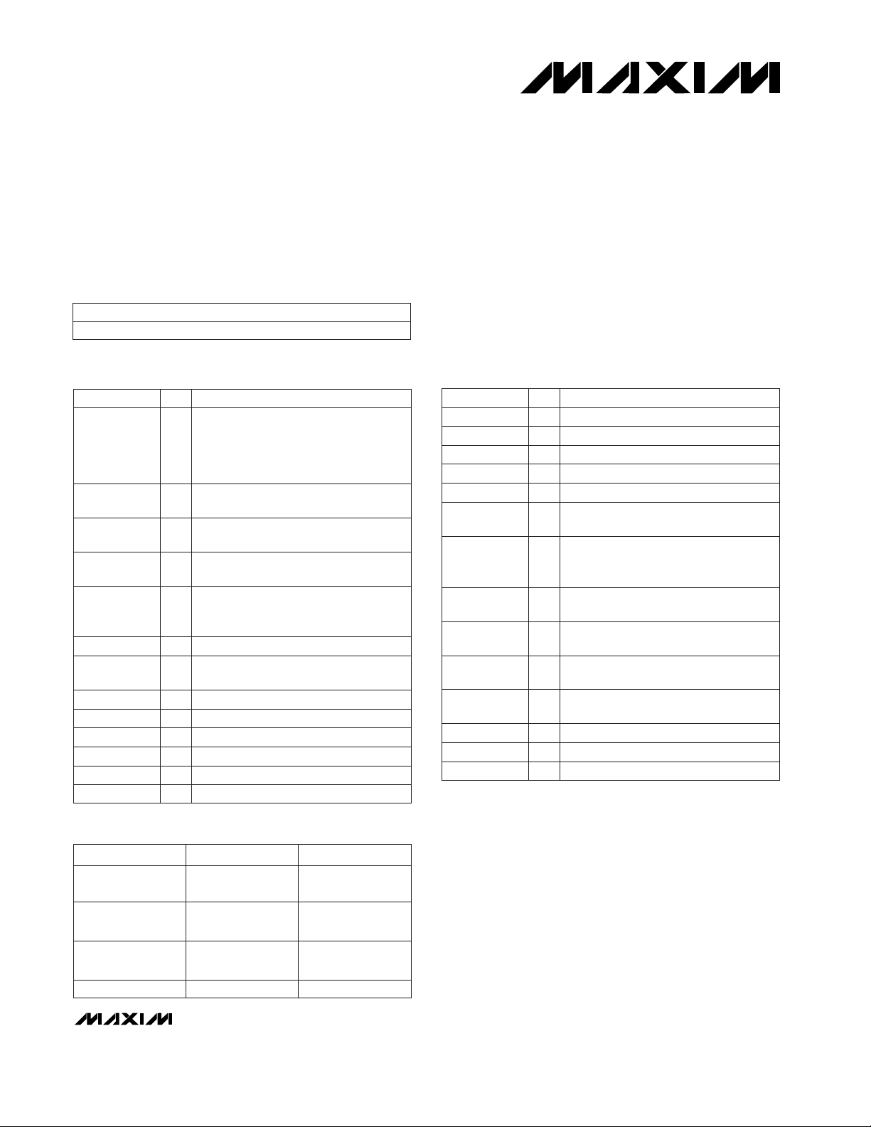
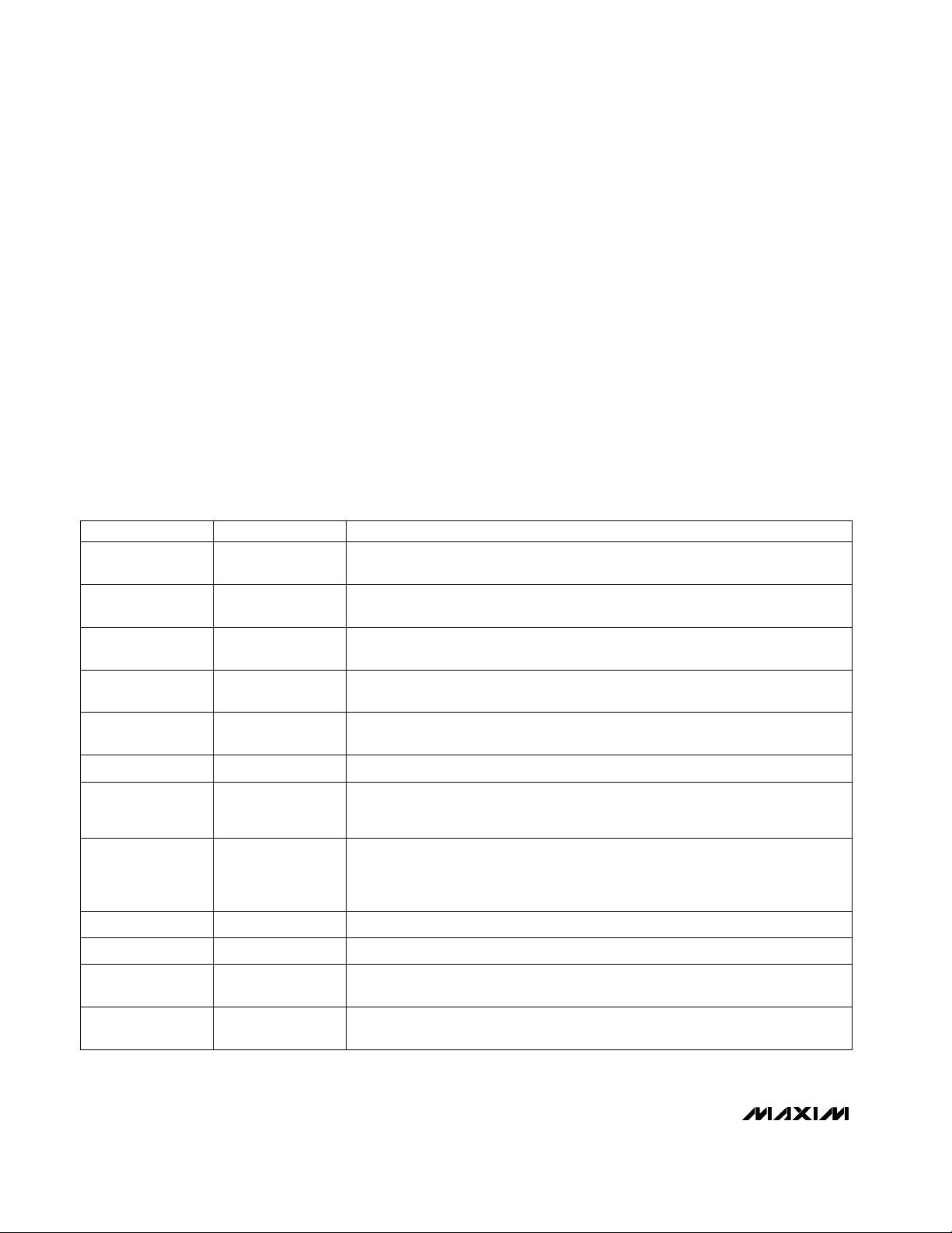
FOUR SOLDER WIRE CONTACTS:
2 TOP (LASER) AND
2 BOTTOM (MONITOR)
SMA CONNECTORS
VIEW FROM TOP
V
CC
LASER ANODE
CONNECTION
MONITOR CATHODE
CONNECTION
LASER DIODE/MONITOR ASSEMBLY
VIEW FROM BOTTOM
OPTICAL FIBER
V
CC
Figure 1. Attachment of Laser Diode/Monitor to MAX3667 EV Kit

Evaluates: MAX3667
MAX3667 Evaluation Kit
4 _______________________________________________________________________________________
V
CC
V
CC
GND
IMOD
GND
IMOD
GND
PULLUP
IBIAS
GND
GND
GND
BIASSET
APC
MODSET
N.C.
MD
16
25262728293031
R17
49.9Ω
SJ1
R15
2k
R12
20k
C9
0.1µF
C16
0.1µF
C14
1µF
C15
0.1µF
R1
130Ω
R2
130Ω
R9
82Ω
R8
82Ω
C10
0.1µF
C12
0.1µF
C17
0.1µF
C18
100µF
C19
0.1µF
C20
100µF
C4
0.1µF
C3
1nF
C7
0.1µF
LASER MONITOR
C6
1µF
C11
0.01µF
C5
0.1µF
C2
0.1µF
C8
0.1µF
JU3
R4
1.5k
R5
R3
3
3
3
1
1
1
2
2
2
R20
100Ω
R19
232Ω
R6
1.5k
R21
22Ω
R11
4.7Ω
R7
100Ω
L1
470nH
C13
0.1µF
C1
0.1µF
3
2
1
JU1
R13
SJ5
+3.3V
SJ4
1 3
2
SJ2
SMA
+3.3V
+3.3V
+3.3V
+3.3V
+3.3V
+3.3V
+3.3V
VFORCE
VFORCE
+3.3V
GND
SMA
J1
J2
J4
SMA
MODMON
MODSET
DISABLE
APC
BIASSET
BIASMON
APCSET
J3
SMA
R18
49.9Ω
VFORCE
JU10
32
1514131211109
1
2 3 5 64 7 8
24
23 22 20 1921 18 17
N.C.
APCSET
N.C.
BIASMON
MODMON
N.C.
COMP
MAX3667
U1
V
CC
V
CC
GND
IN+
IN-
GND
DISABLE
GND
Figure 2. MAX3667 EV Kit Schematic

Evaluates: MAX3667
MAX3667 Evaluation Kit
_______________________________________________________________________________________ 5
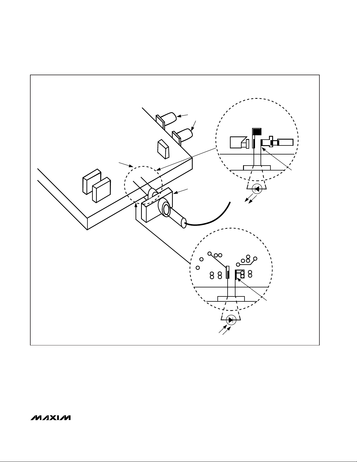
Figure 3. MAX3667 EV Kit Component Placement Guide
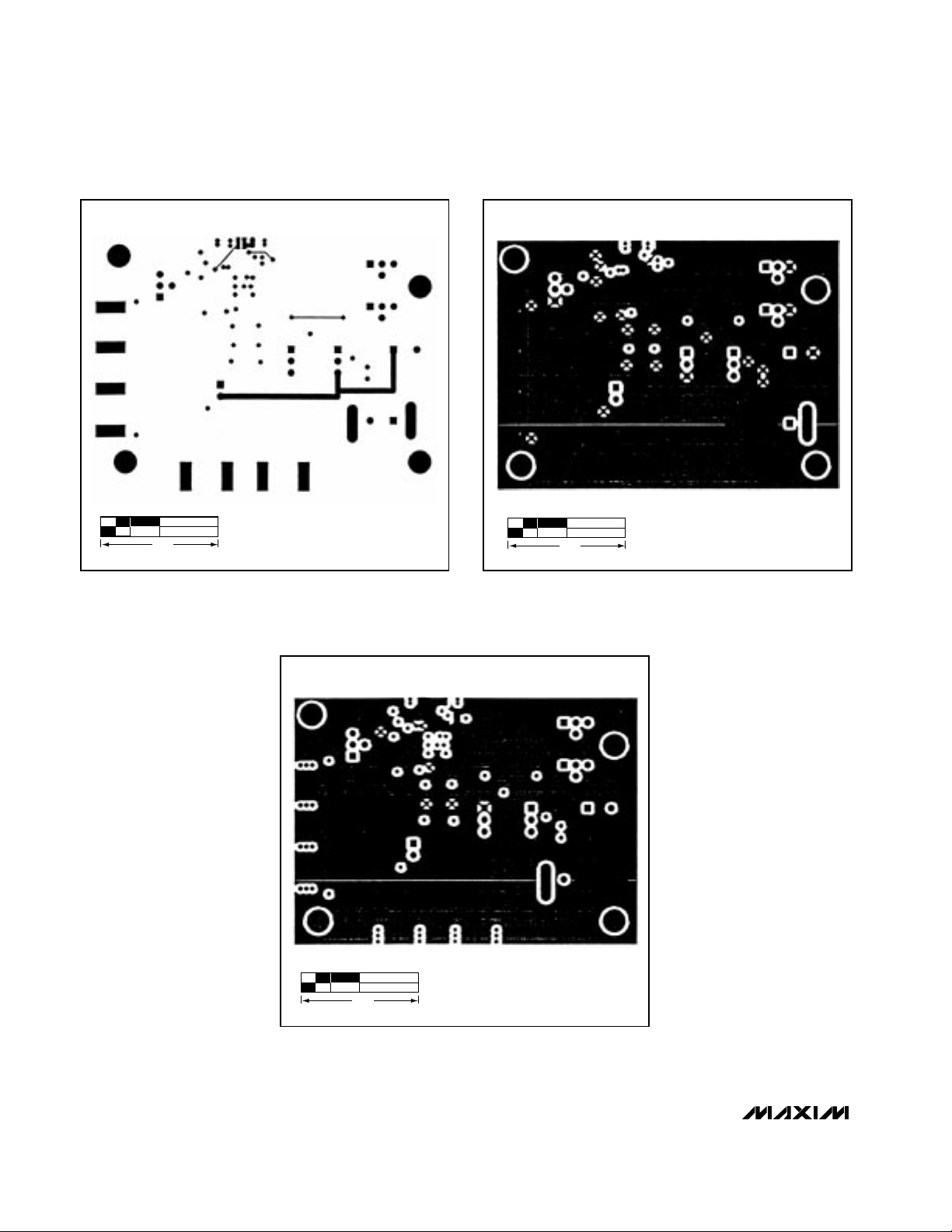
Figure 4. MAX3667 PC Board Layout—Top Solder Mask
1.0"
1.0"
Evaluates: MAX3667
MAX3667 Evaluation Kit
6 _______________________________________________________________________________________
Figure 7. MAX3667 PC Board Layout—Power Plane
1.0"
Figure 5. MAX3667 PC Board Layout—Solder Side
Figure 6. MAX3667 PC Board Layout—GND Plane
1.0"
1.0"

Evaluates: MAX3667
MAX3667 Evaluation Kit
_______________________________________________________________________________________ 7
Figure 9. MAX3667 PC Board Layout—Bottom Solder Mask
1.0"
Figure 8. MAX3667 PC Board Layout—Component Side
1.0"

Maxim cannot assume responsibility for use of any circuitry other than circuitry entirely embodied in a Maxim product. No circuit patent licenses are
implied. Maxim reserves the right to change the circuitry and specifications without notice at any time.
8
_____________________Maxim Integrated Products, 120 San Gabriel Drive, Sunnyvale, CA 94086 408-737-7600
© 1998 Maxim Integrated Products Printed USA is a registered trademark of Maxim Integrated Products.
Evaluates: MAX3667
MAX3667 Evaluation Kit
NOTES
 Loading...