

For free samples & the latest literature: http://www.maxim-ic.com, or phone 1-800-998-8800.
For small orders, phone 1-800-835-8769.
19-1601; Rev 0; 1/00
________________General Description
The MAX3665 low-power transimpedance preamplifier
for 622Mbps SDH/SONET applications consumes only
70mW at VCC= 3.3V. Operating from a single +3.3V or
+5.0V supply, it converts a small photodiode current to a
measurable differential voltage. A DC cancellation circuit
provides a true differential output swing over a wide
range of input current levels, thus reducing pulse-width
distortion. The differential outputs are back-terminated
with 50Ω per side.
The overall transimpedance gain is nominally 8kΩ. For
input signal levels beyond approximately 50µAp-p, the
amplifier will limit the output swing to 250mV. The
MAX3665’s low 55nA input noise provides a typical
sensitivity of -33.2dBm in 1300nm, 622Mbps receivers.
The MAX3665 is designed to be used in conjunction
with the MAX3676 clock recovery and data retiming IC
with limiting amplifier. Together they form a complete
3.3V or 5.0V 622Mbps SDH/SONET receiver.
In die form, the MAX3665 is designed to fit on a header
with a PIN diode. It includes a filter connection that provides positive bias for the photodiode through a 1.5kΩ
resistor to VCC. The device is available in an 8-pin
µMAX package.
________________________Applications
SDH/SONET Receivers
PIN Photodiode Preamplifiers and Receivers
Regenerators for SDH/SONET
____________________________Features
♦ +3.3V or +5.0V Single-Supply Operation
♦ 55nA
RMS
Input-Referred Noise
♦ 70mW Power Consumption at V
CC
= 3.3V
♦ 8kΩ Gain
♦ 450µA Peak Input Current
♦ 260ps max Deterministic Jitter
♦ Differential Output Drives 100Ω Load
♦ 470MHz Bandwidth
MAX3665
622Mbps, Ultra-Low-Power, 3.3V
Transimpedance Preamplifier for SDH/SONET
________________________________________________________________ Maxim Integrated Products 1
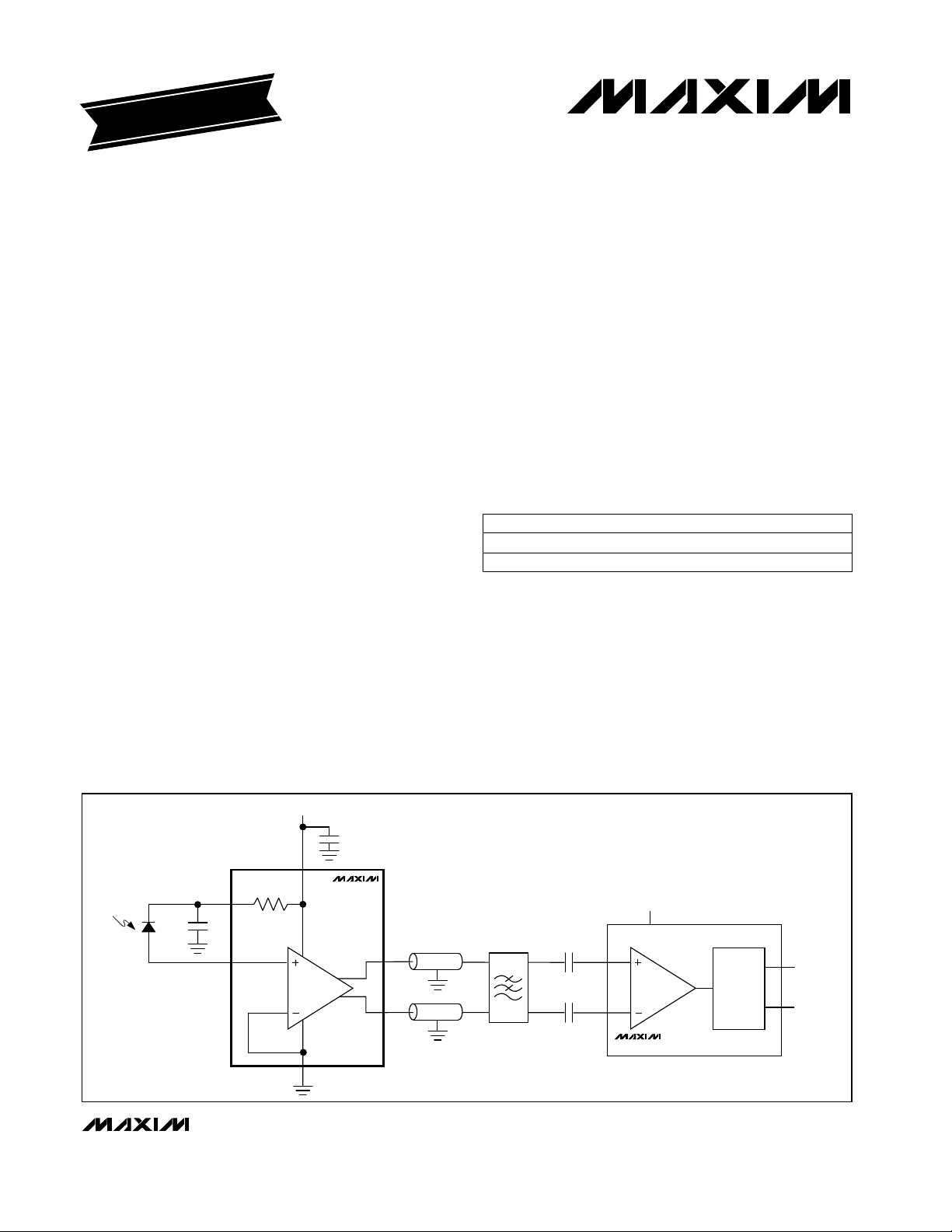
__________________________________________________Typical Application Circuit
PART
MAX3665EUA -40°C to +85°C
TEMP. RANGE PIN-PACKAGE
8 µMAX
EVALUATION KIT
AVAILABLE
_______________Ordering Information
Pin Configuration appears at end of data sheet.
Note: Dice are designed to operate over a -40°C to +140°C
junction temperature (T
j
) range, but are tested and guaranteed
at T
A
= +25°C.
MAX3665E/D (see Note) Dice
C
FILT
FILT
IN
R
1.5k
FILT
3.3V
0.01µF
V
CC
GND
MAX3665
OUT+
OUT-
50Ω
50Ω
0.1µF
0.1µF
3.3V
LIMITING
MAX3676
AMP
CLOCK
AND
DATA
RECOVERY
CLK
DATA
MAX3665
622Mbps, Ultra-Low-Power, 3.3V
Transimpedance Preamplifier for SDH/SONET
2 _______________________________________________________________________________________
ABSOLUTE MAXIMUM RATINGS
DC ELECTRICAL CHARACTERISTICS
(VCC= +3.3V ±10% or +5.0V ±10%, 100Ω load between OUT+ and OUT-, TA= -40°C to +85°C. Typical values are at VCC= +3.3V,
T
A
= +25°C, unless otherwise noted.)
AC ELECTRICAL CHARACTERISTICS
(VCC= +3.3V ±10% or +5.0V ±10%, 100Ω load between OUT+ and OUT-, source capacitance = 0.5pF, TA= -40°C to +85°C. Typical
values are at V
CC
= +3.3V, TA= +25°C, unless otherwise noted.) (Notes 1 and 2)
Stresses beyond those listed under “Absolute Maximum Ratings” may cause permanent damage to the device. These are stress ratings only, and functional
operation of the device at these or any other conditions beyond those indicated in the operational sections of the specifications is not implied. Exposure to
absolute maximum rating conditions for extended periods may affect device reliability.
Note 1: AC characteristics are guaranteed by design.
Note 2: Measured with a 3-pole filter at the output. C
IN
= 0.5pF, IIN= 0, C
FILT
= 1000pF.
Note 3: PSRR = -20log (∆V
OUT
/ ∆VCC).
V
CC
........................................................................-0.5V to +6.5V
Continuous Current at IN ....................................................±5mA
Voltage at OUT+, OUT- ...................(V
CC
- 1.5V) to (VCC+ 0.5V)
Voltage at FILT ...........................................-0.5V to (VCC+ 0.5V)
Continuous Power Dissipation (T
A
= +85°C)
8-Pin µMAX (derate 4.5mW/°C above +85°C) ...........295mW
Operating Junction Temperature (die) ..............-55°C to +150°C
Processing Temperature (die) .........................................+400°C
Storage Temperature Range .............................-55°C to +150°C
Lead Temperature (soldering, 10s) .................................+300°C
I
IN
= 0
IIN= 0 to 10µAp-p
IIN= 0 to 300µA
IIN= 450µAp-p
Differential output
IIN= 300µA
CONDITIONS
mA
21 30
I
CC
Supply Current
%
±5
V
0.8 0.95
V
IN
Input Bias Voltage
Gain Nonlinearity
kΩ
1.5
R
FILT
Filter Resistor
mVp-p
260 450
V
OUT(MAX)
Maximum Output Voltage
kΩ
78
z
21
Small-Signal Transimpedance
V
VCC- 0.15
Output Common-Mode Voltage
mV
±5
∆V
OUT
Differential Output Offset
Ω
48 50 52
Z
OUT
Output Impedance (per side)
UNITSMIN TYP MAXSYMBOLPARAMETER
-3dB with IIN= 5µA
Relative to gain at 10MHz
2
13
- 1 PRBS with 100 CIDs
CONDITIONS
kHz
20 40
MHz
404 470
BW
-3dB
Small-Signal Bandwidth
Low-Frequency Cutoff
100 260
psJ
D
Deterministic Jitter
UNITSMIN TYP MAXSYMBOLPARAMETER
RMS Noise Referred to Input i
n
55 72
nA
Power-Supply Rejection Ratio PSRR
f < 1MHz, differential referred to output,
∆VCC= 30mVp-p (Note 3)
36 47
dB
MAX3665
622Mbps, Ultra-Low-Power, 3.3V
Transimpedance Preamplifier for SDH/SONET
_______________________________________________________________________________________ 3
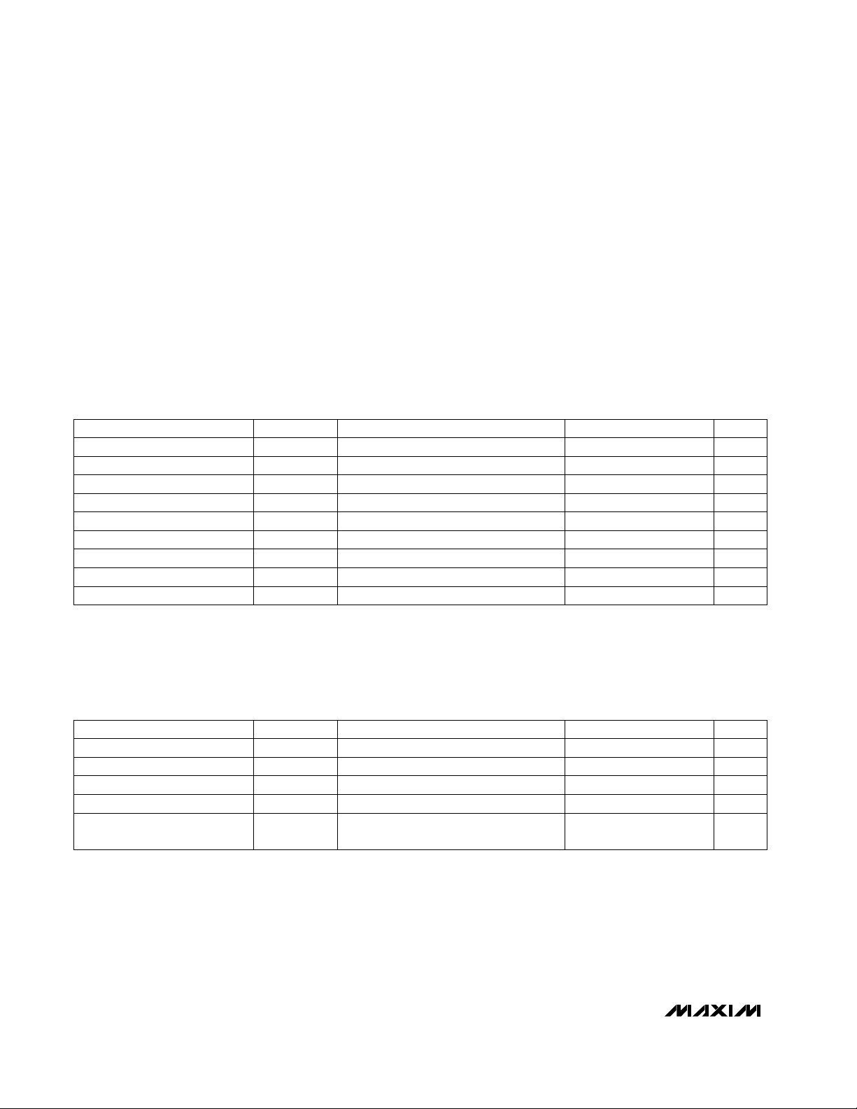
__________________________________________Typical Operating Characteristics
(VCC= +3.3V, includes off-chip filter, see Figure 3b, TA= +25°C, unless otherwise noted.)
INPUT-REFERRED NOISE
vs. TEMPERATURE
100
90
80
70
60
50
40
30
RMS NOISE CURRENT (nA)
20
10
0
-40 -20 0 20 40 60 80 100
C
= 1.5pF
IN
C
= 1pF
IN
C
= 0.5pF
IN
CIN IS SOURCE CAPACITANCE PRESENTED TO
DIE. IINCLUDES PACKAGE PARASITIC,
PIN DIODE, AND PARASITIC INTERCONNECT
CAPACITANCE.
JUNCTION TEMPERATURE (°C)
INPUT-REFERRED NOISE
vs. DC INPUT CURRENT
250
SOURCE CAPACITANCE = 0.5pF
200
150
100
RMS NOISE CURRNENT (nA)
50
0
0.1 1 10
DC INPUT CURRENT (µA)
100 1000
MAX3665 TOC01
MAX3665 toc04
SMALL-SIGNAL GAIN
vs. FREQUENCY
79
78
77
76
75
74
GAIN (dB)
73
72
71
70
69
10k 100k 1M 10M 100M 1G
FREQUENCY (Hz)
SMALL-SIGNAL TRANSIMPEDANCE
vs. TEMPERATURE
TRANSIMPEDANCE (Ω)
8100
8000
7900
7800
7700
7600
7500
7400
VCC = 5.0V
VCC = 3.3V
-40 0 20-20 40 60 80 100
AMBIENT TEMPERATURE (°C)
MAX3665 toc02
PWD (ps)
MAX3665 toc05
PWD (ps)
PULSE-WIDTH DISTORTION vs.
TEMPERATURE (INPUT = 100µAp-p)
50
45
40
35
30
25
20
15
VCC = 3.3V
10
5
0
-40 -20 0 20 40 60 80 100
AMBIENT TEMPERATURE (°C)
VCC = 5.0V
PULSE-WIDTH DISTORTION vs.
TEMPERATURE (INPUT = 450µAp-p)
50
45
40
35
30
25
20
15
10
5
0
-40 -20 0 20 40 60 80 100
V
= 3.3V
CC
V
= 5.0V
CC
AMBIENT TEMPERATURE (°C)
MAX3665 toc03
MAX3665 toc06
BANDWIDTH vs. TEMPERATURE
575
V
= 3.3V or 5.0V
CC
550
525
500
475
BANDWIDTH (MHz)
450
425
400
-40 0 20-20 40 60 80 100
AMBIENT TEMPERATURE (°C)
160
140
MAX2665 toc07
120
100
80
60
PEAK-TO-PEAK JITTER (ps)
40
20
0
DATA-DEPENDENT JITTER
vs. INPUT SIGNAL AMPLITUDE
VCC = 3.3V
VCC = 5.0V
0 150 20050 100 250 300 350 400 450
PEAK-TO-PEAK AMPLITUDE (µA)
OUTPUT COMMON-MODE VOLTAGE
(REFERENCED TO V
-0.10
-0.11
MAX3665-08
-0.12
-0.13
-0.14
-0.15
-0.16
-0.17
COMMON-MODE VOLTAGE (V)
-0.18
-0.19
-0.20
-40 -20 0 20 40 60 80 100
) vs. TEMPERATURE
CC
V
= 3.3V
CC
V
= 5.0V
CC
AMBIENT TEMPERATURE (°C)
MAX3665 toc09
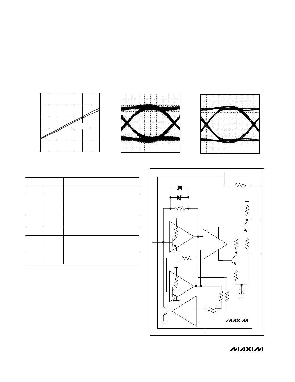
________________Detailed Description
The MAX3665 is a transimpedance amplifier designed
for 622Mbps SDH/SONET applications. It comprises a
transimpedance amplifier, a paraphase amplifier with
CML differential outputs, and a DC cancellation loop.
Figure 1 shows a functional diagram of the MAX3665.
Transimpedance Amplifier
The signal current at IN flows into the summing node of a
high-gain amplifier. Shunt feedback through RFconverts
this current to a voltage. Diodes D1 and D2 clamp the
output voltage for large input currents.
MAX3665
622Mbps, Ultra-Low-Power, 3.3V
Transimpedance Preamplifier for SDH/SONET
4 _______________________________________________________________________________________
_____________________________Typical Operating Characteristics (continued)
(VCC= +3.3V, includes off-chip filter, see Figure 3b, TA= +25°C, unless otherwise noted.)
150
200
300
250
350
400
-40 0-20 20 40 60 80 100
DIFFERENTIAL OUTPUT AMPLITUDE
vs. TEMPERATURE (INPUT = 450µAp-p)
MAX3665 toc10
AMBIENT TEMPERATURE (°C)
PEAK-TO-PEAK AMPLITUDE (mV)
VCC = 5.0V
VCC = 3.3V
EYE DIAGRAM
(INPUT = 10µAp-p)
15mV/div
MAX3665-11
200ps/div
INPUT: 213 - 1 PRBS
CONTAINS 100 ZEROS
EYE DIAGRAM
(INPUT = 450µAp-p)
50mV/div
MAX3665-12
200ps/div
INPUT: 213 - 1 PRBS
CONTAINS 100 ZEROS
_____________________Pin Description
NAME FUNCTION
1
V
CC
+3.3V or +5.0V Supply Voltage
2 IN Signal Input (from photodiode)
PIN
3 N.C.
No Connection. Not internally connected.
4 FILT
On-Chip Resistor for Filtering
Photodiode Supply Voltage
7 OUT-
Inverting Voltage Output. Current flowing into IN causes V
OUT-
to decrease.
6 OUT+
Noninverting Voltage Output. Current
flowing into IN causes V
OUT+
to
increase.
5, 8 GND Ground
Figure 1. Functional Diagram
V
AMP
CC
1.5k
R1
50Ω
V
CC
R2
R5
50Ω
Q3
D2
D1
R
F
V
CC
IN
Q1
R7
V
CC
PARAPHASE
FILT
V
CC
OUT+
Q2
OUT-
Q5
Q4
REFERENCE AMP
DC
CANCELLATION
AMP
GND
R6
R4
R3
MAX3665

Paraphase Amplifier
The paraphase amplifier converts single-ended inputs to
differential outputs, and introduces a voltage gain. This
signal drives a differential pair of transistors, Q2 and Q3,
which form the output stage. Resistors R1 and R2 provide
back-termination at the output, absorbing reflections
between the MAX3665 and its load.
The differential outputs are designed to drive a 100Ω
load between OUT+ and OUT-. They can also drive
higher output impedances, resulting in increased gain
and output voltage swing.
DC Cancellation Loop
The DC cancellation loop removes the DC component
of the input signal by using low-frequency feedback.
This feature centers the signal within the MAX3665’s
dynamic range, reducing pulse-width distortion on
large input signals.
The output of the transimpedance amplifier is sensed
through resistors R3 and R4 and then filtered, amplified,
and fed back to the base of transistor Q4. The transistor
draws the DC component of the input signal away from
the transimpedance amplifier’s summing node.
Connect a 400pF or larger capacitor (C
FILT
) between
FILT and case ground for TO header, die-mounted operation. Increasing C
FILT
improves PSRR. The DC cancel-
lation loop can sink up to 300µA of current at the input.
The MAX3665 minimizes pulse-width distortion for data
sequences that exhibit a 50% mark density. A mark
density other than 50% causes the device to generate
pulse-width distortion.
DC cancellation current is drawn from the input and
adds noise. For low-level signals with little or no DC
component, this is not a problem. Preamplifier noise will
increase for signals with a significant DC component.
___________Applications Information
The MAX3665 is a low-noise, wide-bandwidth transimpedance amplifier that is ideal for 622Mbps SDH/
SONET receivers. Its features allow easy design into a
fiber optic module, in three simple steps.
Step 1: Selecting a Preamplifier for a 622Mbps
Receiver
Fiber optic systems place requirements on the bandwidth, gain, and noise of the transimpedance preamplifier. The MAX3665 optimizes these characteristics for
SDH/SONET receiver applications that operate at
622Mbps.
In general, the bandwidth of a fiber optic preamplifier
should be 0.6 to 1 times the data rate. Therefore, in a
622Mbps system, the bandwidth should be between
375MHz and 622MHz. Lower bandwidth causes pattern-dependent jitter and a lower signal-to-noise ratio,
while higher bandwidth increases thermal noise. The
MAX3665 typical bandwidth is 470MHz, making it ideal
for 622Mbps applications.
The preamplifier’s transimpedance must be high
enough to ensure that expected input signals generate
output levels exceeding the sensitivity of the limiting
amplifier (quantizer) in the following stage. The
MAX3676 clock recovery and limiting amplifier IC has an
input sensitivity of 3.6mVp-p, which means that
3.6mVp-p is the minimum signal amplitude required to
produce a fully limited output. Therefore, when used
with the MAX3665, which has an 8kΩ transimpedance,
the minimum detectable photodetector current is
450nAp-p.
It is common to relate peak-to-peak input signals to
average optical power. The relationship between optical input power and output current for a photodetector
is called the responsivity (ρ), with units amperes per
watt (A/W). The photodetector peak-to-peak current is
related to the peak-to-peak optical power as follows:
Ip-p = (Pp-p)(ρ)
Based on the assumption that SDH/SONET signals
maintain a 50% mark density, the following equations
relate peak-to-peak optical power to average optical
power and extinction ratio (Figure 2):
Average Optical Power = P
AVG
= (P0 + P1) / 2
Extinction Ratio = re= P1 / P0
Peak-to-Peak Signal Amplitude = Pp-p = P1 - P0
MAX3665
622Mbps, Ultra-Low-Power, 3.3V
Transimpedance Preamplifier for SDH/SONET
_______________________________________________________________________________________ 5
Figure 2. Optical Power Definitions
POWER
P1
P
AVG
P0
TIME

MAX3665
Therefore,
P
AVG
= Pp-p (1 / 2)[(re+ 1) / (re- 1)]
Sensitivity is a key specification of the receiver module.
The ITU/Bellcore specifications for SDH/SONET
receivers require a link sensitivity of -27dBm with a bit
error rate (BER) of 10
-10
. There is an additional 1dB
power penalty to accommodate various system losses;
therefore, the sensitivity of a 622Mbps receiver must be
better than -28dBm.
Although several parameters affect sensitivity (such as
the quantizer sensitivity and preamplifier gain, as previously discussed), most fiber optic receivers are designed
so that noise is the dominant factor. Noise from the highgain transimpedance amplifier, in particular, determines
the sensitivity. The noise generated by the MAX3665 can
be modeled with a Gaussian distribution. In this case, a
BER of 10
-10
corresponds to a peak-to-peak signal
amplitude to RMS noise ratio (SNR) of 12.7. The
MAX3665’s typical input-referred noise, in, (bandwidthlimited to 470MHz) is 55nA
RMS
. Therefore, the minimum
input for a BER of 10
-10
is (12.7 · 55nA) = 699nAp-p.
Rearranging the previous equations in these terms
results in the following relationship:
Optical Sensitivity (dBm) =
10log[(in/ ρ)(SNR)(1/2)(re+ 1) / (re- 1)(1000)]
At room temperature, with re= 10, SNR = 12.7, in=
55nA, and ρ = 0.9A/W, the MAX3665 sensitivity is
-33.2dBm. For worst-case conditions, noise increases
to 72nA and sensitivity decreases to -32.1dBm. The
MAX3665 provides 5.1dB margin over the SDH/SONET
specifications, even at +85°C.
The MAX3665’s overload current (I
MAX
) is greater than
450µAp-p. The pulse-width distortion and input current
are closely related. If the clock recovery circuit can
accept more pulse-width distortion, a higher input current
might be acceptable. For worst-case responsivity and
extinction ratio, ρ = 1A/W and r
e
= ∞, the input overload
is:
Overload (dBm) = -10log (I
MAX
)(1 / 2)(1000)
For I
MAX
= 450µA, the MAX3665 overload is -6.5dBm.
Step 2: Designing Filters
The MAX3665’s noise performance is a strong function
of the circuit’s bandwidth, which changes over temperature and varies from lot to lot. The receiver sensitivity
can be improved by adding filters to limit this bandwidth. Filter designs can range from a one-pole filter
using a single capacitor, to more complex filters using
inductors. Figure 3 illustrates two examples: the simple
filter provides moderate roll-off with minimal compo-
nents, while the complex filter provides a sharper rolloff. Parasitics on the PC board will affect the filter characteristics. Refer to the MAX3665 EV kit data sheet for a
layout example of the filter shown in Figure 3b.
Supply voltage noise at the cathode of the photodiode
produces a current I = C
PHOTO
(∆V/∆t), which reduces
the receiver sensitivity. C
PHOTO
is the photodiode
capacitance.
The FILT resistor of the MAX3665, combined with an
external capacitor (see Typical Operating Circuit) can
be used to reduce this noise. The external capacitor
(C
FILT
) is placed in parallel with the photodiode.
Current generated by supply noise is divided between
C
FILT
and C
PHOTO
. The input noise current due to supply noise is (assuming the filter capacitor is much larger
than the photodiode capacitance):
622Mbps, Ultra-Low-Power, 3.3V
Transimpedance Preamplifier for SDH/SONET
6 _______________________________________________________________________________________
Figure 3. Filter Design Examples
VC
()( )
I
NOISE
a) SIMPLE, 1-POLE, 530MHz FILTER
MAX3665
50Ω
1.2pF
50Ω
b) 3-POLE, 515MHz FILTER
MAX3665
50Ω
1.2pF
50Ω
NOISE PHOTO
=
RC
()()
FILT FILT
C1
5pF
22nH
4pF 5pF
22nH
REFER TO THE MAX3665 EV KIT DATA SHEET
FOR THE FILTER LAYOUT EXAMPLE.
R
L
100Ω
R
L
100Ω

If the amount of tolerable noise is known, then the filter
capacitor can be easily selected:
For example, with maximum noise voltage = 100mVp-p,
C
PHOTO
= 0.5pF, R
FILT
= 1.5kΩ, and I
NOISE
selected
to be 6nA (1/10 of MAX3665 input-referred noise):
Figure 4 shows the suggested layout for a TO-46 header
Step 3: Designing a Low-Capacitance Input
Noise performance and bandwidth are adversely
affected by stray capacitance on the input node. Select
a low-capacitance photodiode and use good high-frequency design and layout techniques to minimize
capacitance on this pin. The MAX3665 is optimized for
0.5pF of capacitance on the input—approximately the
capacitance of a photodetector diode sharing a common header with the MAX3665 in die form.
Photodiode capacitance changes significantly with bias
voltage. With a +3.3V supply voltage, the reverse voltage
on the PIN diode is only 2.5V. If a higher voltage supply
is available, apply it to the diode to significantly reduce
capacitance.
Take great care to reduce input capacitance. With the
µMAX version of the MAX3665, the package capacitance is about 0.3pF, and the PC board between the
MAX3665 input and the photodiode can add parasitic
capacitance. Keep the input line short, and remove
power and ground planes beneath it. Packaging the
MAX3665 into a header with the photodiode provides
the best possible performance. It reduces parasitic
capacitance to a minimum, resulting in the lowest noise
and the best bandwidth.
Wire Bonding
For high current density and reliable operation, the
MAX3665 uses gold metallization. Make connections to
the die with gold wire only, and use ball-bonding techniques (wedge-bonding is not recommended). Die-pad
size is 4 mils square. Die thickness is 12 mils.
VCCand Ground
Use good high-frequency design and layout techniques. The use of a multilayer circuit board with separate ground and V
CC
planes is recommended. Take
care to bypass V
CC
and to connect the GND pin to the
ground plane with the shortest possible traces.
MAX3665
622Mbps, Ultra-Low-Power, 3.3V
Transimpedance Preamplifier for SDH/SONET
_______________________________________________________________________________________ 7
C =
FILT
C = 0.1
FILT
()
()
V
()( )
NOISE
()( )
−−
⋅⋅
0 5 10 1500 6 10 5 6
. / . nF
C
PHOTO
RI
FILT NOISE
12 4
()
()
=

MAX3665
622Mbps, Ultra-Low-Power, 3.3V
Transimpedance Preamplifier for SDH/SONET
8 _______________________________________________________________________________________
Figure 4. Suggested Layout for TO-46 Header
V
CC
FILTER CAP
OUT+
IN V
FILT
GND
OUT+ OUT-
CC
GND
OUT-

MAX3665
622Mbps, Ultra-Low-Power, 3.3V
Transimpedance Preamplifier for SDH/SONET
_______________________________________________________________________________________ 9
___________________Pin Configuration ___________________Chip Topography
TRANSISTOR COUNT: 443
SUBSTRATE CONNECTED TO GND
TOP VIEW
V
N.C.
FILT
1
CC
2
IN
MAX3665
3
4
µMAX
8
GND
OUT-
7
OUT+
6
5
GND
GND
FILT IN V
IN
CC
GND
0.05"
(1.27mm)
OUT+ OUT-
0.03"
(0.76mm)

MAX3665
622Mbps, Ultra-Low-Power, 3.3V
Transimpedance Preamplifier for SDH/SONET
10 ______________________________________________________________________________________
________________________________________________________Package Information
8LUMAXD.EPS

MAX3665
622Mbps, Ultra-Low-Power, 3.3V
Transimpedance Preamplifier for SDH/SONET
______________________________________________________________________________________ 11
NOTES

MAX3665
622Mbps, Ultra-Low-Power, 3.3V
Transimpedance Preamplifier for SDH/SONET
Maxim cannot assume responsibility for use of any circuitry other than circuitry entirely embodied in a Maxim product. No circuit patent licenses are
implied. Maxim reserves the right to change the circuitry and specifications without notice at any time.
12 ____________________Maxim Integrated Products, 120 San Gabriel Drive, Sunnyvale, CA 94086 408-737-7600
© 2000 Maxim Integrated Products Printed USA is a registered trademark of Maxim Integrated Products.
NOTES
 Loading...