Maxim MAX3664E-D, MAX3664EUA, MAX3664ESA Datasheet

For free samples & the latest literature: http://www.maxim-ic.com, or phone 1-800-998-8800.
For small orders, phone 408-737-7600 ext. 3468.
19-0479; Rev 1; 7/97
________________General Description
The MAX3664 low-power transimpedance preamplifier
for 622Mbps SDH/SONET applications consumes only
85mW. Operating from a single +3.3V supply, it converts
a small photodiode current to a measurable differential
voltage. A DC cancellation circuit provides a true differential output swing over a wide range of input current
levels, thus reducing pulse-width distortion. The differential outputs are back-terminated with 60Ω per side.
The transimpedance gain is nominally 6kΩ. For input
signal levels beyond approximately 100µAp-p, the
amplifier will limit the output swing to 900mV. The
MAX3664’s low 55nA input noise provides a typical
sensitivity of -33.2dBm in 1300nm, 622Mbps receivers.
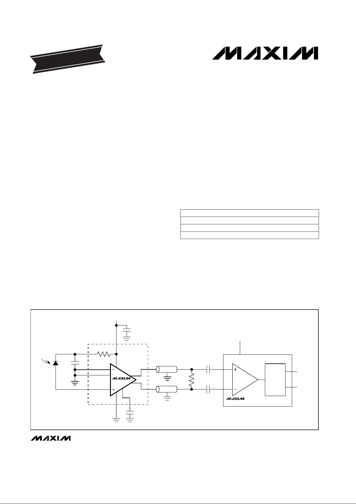
The MAX3664 is designed to be used in conjunction
with the MAX3675 clock recovery and data retiming IC
with limiting amplifier. Together, they form a complete
3.3V, 622Mbps SDH/SONET receiver.
In die form, the MAX3664 is designed to fit on a header
with a PIN diode. It includes a filter connection, which
provides positive bias for the photodiode through a 1kΩ
resistor to VCC. The device is also available in 8-pin SO
and µMAX packages.
________________________Applications
SDH/SONET Receivers
PIN/Preamplifier Receivers
Regenerators for SDH/SONET
____________________________Features
♦ Single +3.3V Supply Operation
♦ 55nA
RMS
Input-Referred Noise
♦ 6kΩ Gain
♦ 85mW Power
♦ 300µA Peak Input Current
♦ 200ps Max Pulse-Width Distortion
♦ Differential Output Drives 100Ω Load
♦ 590MHz Bandwidth
MAX3664
622Mbps, Ultra-Low-Power, 3.3V
Transimpedance Preamplifier for SDH/SONET
________________________________________________________________
Maxim Integrated Products
1
MAX3664
MAX3675
LIMITING
AMP
100pF
INREF2
1k
V
CC
100Ω
0.01µF
47nF
VCC (+3.3V)
DATA
CLK
( ) ARE FOR MAX3664E/D (DICE) ONLY.
47nF
400pF
OUT+
OUT-
COMP
GND
V
CC
(+3.3V)
(FILT)
INREF1
IN
DATA
AND
CLOCK
RECOVERY
__________________________________________________Typical Application Circuit
PART
MAX3664E/D
MAX3664ESA
MAX3664EUA* -40°C to +85°C
-40°C to +85°C
-40°C to +85°C
TEMP. RANGE PIN-PACKAGE
Dice
8 SO
8 µMAX
EVALUATION KIT
AVAILABLE
_______________Ordering Information
Pin Configuration appears at end of data sheet.
* Contact factory for package availability.

MAX3664
622Mbps, Ultra-Low-Power, 3.3V
Transimpedance Preamplifier for SDH/SONET
2 _______________________________________________________________________________________
ABSOLUTE MAXIMUM RATINGS
DC ELECTRICAL CHARACTERISTICS
(VCC= +3.3V ±0.3V, COMP = GND, 100Ω load between OUT+ and OUT-, TA= -40°C to +85°C. Typical values are at TA= +25°C,
unless otherwise noted.) (Notes 1, 2)
AC ELECTRICAL CHARACTERISTICS
(VCC= +3.3V ±0.3V, C
COMP
= 400pF, CIN= 1.1pF, outputs terminated into 50Ω, 8-pin SO package in MAX3664 EV board,
TA= +25°C, unless otherwise noted.) (Notes 3, 4)
Stresses beyond those listed under “Absolute Maximum Ratings” may cause permanent damage to the device. These are stress ratings only, and functional
operation of the device at these or any other conditions beyond those indicated in the operational sections of the specifications is not implied. Exposure to
absolute maximum rating conditions for extended periods may affect device reliability.
Note 3: AC Characteristics are guaranteed by design.
Note 4: C
IN
is the total capacitance at IN.
Note 5: PWD =
|
2 x Pulse width - Period
|
2
Note 6: DC to 470MHz, measured with 3-pole Bessel filter at output.
Note 1: Dice are tested at T
j
= +27°C.
Note 2: µMAX package tested at T
A
= +25°C to +85°C.
V
CC
........................................................................-0.5V to +5.5V
Continuous Current
IN, INREF1, INREF2, COMP, FILT....................................5mA
OUT+, OUT-...................................................................25mA
Continuous Power Dissipation (T
A
= +85°C)
SO (derate 5.88mW/°C above +85°C)........................383mW
µMAX (derate 4.1mW/°C above +85°C) .....................268mW
Operating Junction Temperature (die)..............-40°C to +150°C
Processing Temperature (die).........................................+400°C
Storage Temperature Range.............................-65°C to +160°C
Lead Temperature (soldering, 10sec).............................+300°C
I
IN
= 0
IIN= 0 to 20µA
IIN= 0 to 300µA
IIN= 300µA
Differential output
f < 1MHz, referred to output
IIN= 200µA, C
COMP
= 400pF
CONDITIONS
mA12 25 35I
CC
Supply Current
%±5
V0.8 0.95V
IN
Input Bias Voltage
Gain Nonlinearity
mV950V
OUT
(max)Maximum Output Voltage
Ω40 60 75Z
OUT
Output Impedance (per side)
kΩ4.5 6 7.5z
21
Small-Signal Transimpedance
VVCC- 1.3Output Common-Mode Level
dB20PSRRPower-Supply Rejection Ratio
mV±7∆V
OUT
Differential Output Offset
UNITSMIN TYP MAXSYMBOLPARAMETER
Relative to gain at 10MHz
CIN= 1.1pF (Note 6), IIN= 0
2µA to 100µA peak input current,
50% duty cycle, 1–0 pattern
100µA to 300µA peak input current,
50% duty cycle, 1–0 pattern
CIN= 0.3pF (Note 6), IIN= 0
CONDITIONS
kHz150
MHz590BW
-3dB
Small-Signal Bandwidth
Low-Frequency Cutoff
nA
73 86
i
n
RMS Noise Referred to Input
6 100
ps
80 200
PWD
Pulse-Width Distortion
(Note 5)
55
UNITSMIN TYP MAXSYMBOLPARAMETER
Ω800 1000 1200R
FILT
Filter Resistor (die only)

MAX3664
622Mbps, Ultra-Low-Power, 3.3V
Transimpedance Preamplifier for SDH/SONET
_______________________________________________________________________________________
3
100
0
-40 30 100
INPUT-REFERRED NOISE
vs. TEMPERATURE
30
20
40
10
70
90
80
60
MAX3664-01
JUNCTION TEMPERATURE (°C)
NOISE (nA)
-5 65
50
470MHz BANDWIDTH
CIN = 1.5pF
CIN = 0.5pF
CIN = 1.0pF
CIN IS SOURCE CAPACITANCE
PRESENTED TO DIE. INCLUDES PACKAGE
PARASITIC, PIN DIODE, AND PARASITIC
INTERCONNECT CAPACITANCE
80
78
76
10k 100k 10M 10G
SMALL-SIGNAL GAIN
vs. FREQUENCY
62
60
72
70
74
68
MAX3664-02
FREQUENCY (Hz)
GAIN (dB)
1M 100M
64
66
1G
MAX3664 IN EV BOARD
COMP CONNECTED
TO GROUND
COMP CONNECTED
THROUGH 400pF
TO GROUND
200
-50
-40 25 45 85
PULSE-WIDTH DISTORTION
vs. TEMPERATURE
0
100
150
MAX3664-03
AMBIENT TEMPERATURE (°C)
PWD (ps)
-25
0 65
50
IIN = 100µA
IIN = 300µA
MAX3664 IN EV BOARD
1000
0.1 1 10
100
1000
INPUT-REFERRED RMS NOISE CURRENT
vs. DC INPUT CURRENT
MAX3664-04
DC INPUT CURRENT (µA)
RMS NOISE CURRENT (nA)
10
100
C
STC
= 0.5pF
470MHz BANDWIDTH
300
0
0 80 100 120 160
LOW-FREQUENCY CUTOFF
vs. AVERAGE INPUT CURRENT
50
150
250
200
MAX3664-07
AVERAGE INPUT CURRENT (µA)
LOW-FREQUENCY CUTOFF (kHz)
20 40 60 140
100
C
COMP
= 50pF
C
COMP
= 100pF
C
COMP
= 200pF
C
COMP
= 400pF
C
COMP
= 1000pF
6400
5800
-40 30 100
SMALL-SIGNAL TRANSIMPEDANCE
vs. TEMPERATURE
5900
6000
6200
6300
MAX3664-05
JUNCTION TEMPERATURE (°C)
TRANSIMPEDANCE (Ω)
-5 65
6100
VCC = 3V
MEASUREMENT FREQUENCY = 20MHz
VCC = 3.6V
650
400
-40 30 100
BANDWIDTH vs. TEMPERATURE
450
500
550
600
MAX3664-06
JUNCTION TEMPERATURE (°C)
BANDWIDTH (MHz)
-5 65
CIN = 0.5pF
CIN = 1.0pF
CIN = 1.5pF
CIN IS SOURCE CAPACITANCE
PRESENTED TO DIE. INCLUDES PACKAGE
PARASITIC, PIN DIODE, AND PARASITIC
INTERCONNECT CAPACITANCE
120
0
0 150 200 300
DATA-DEPENDENT JITTER
vs. INPUT SIGNAL AMPLITUDE
20
60
100
80
MAX3664-08
PEAK-TO-PEAK AMPLITUDE (µA)
PEAK-TO-PEAK JITTER (ps)
50 100 250
40
C
COMP
= 100pF
C
COMP
= 200pF
C
COMP
= 400pF
C
COMP
= 800pF
EXTINCTION RATIO > 10
INPUT: 213 - 1 PRBS
CONTAINS 72 ZEROS
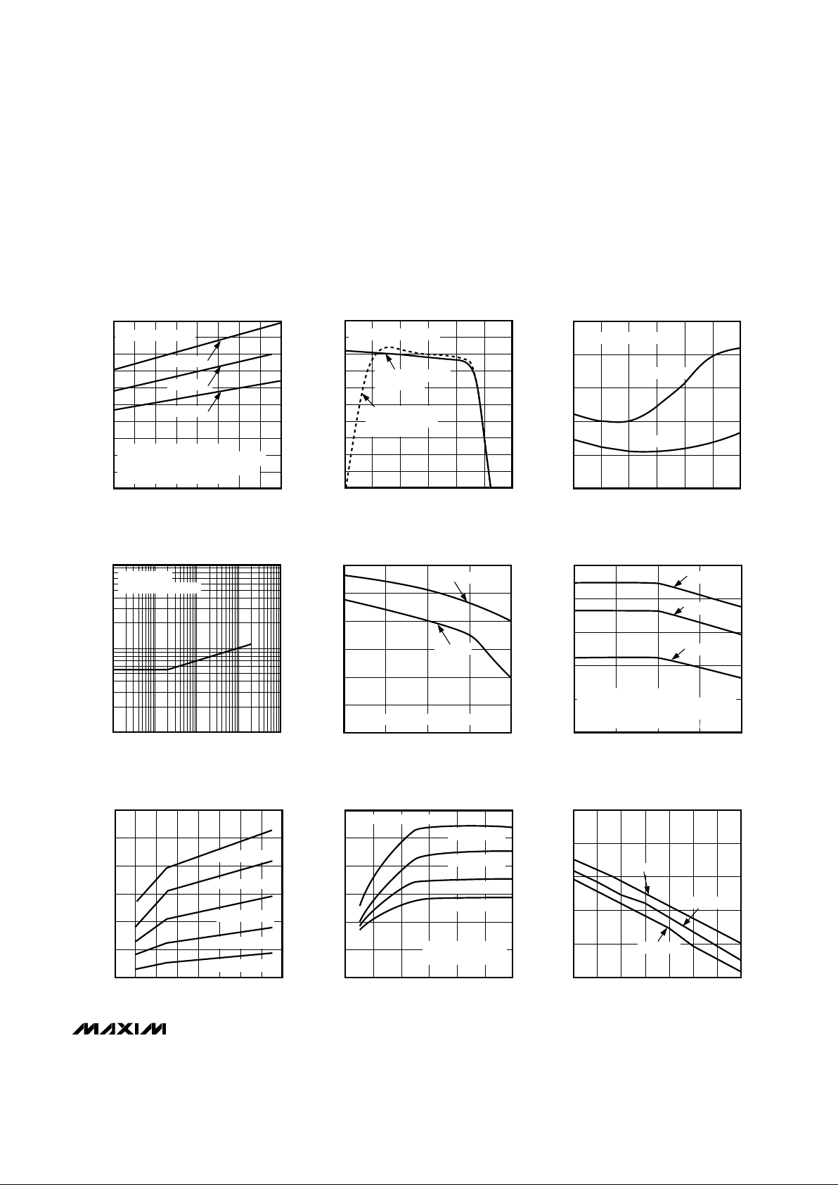
__________________________________________Typical Operating Characteristics
(VCC= +3.3V, C
COMP
= 400pF, TA= +25°C, unless otherwise noted.)
-1.15
-1.40
-40 40 60 100
OUTPUT COMMON-MODE VOLTAGE
(REFERENCED TO V
CC
) vs. TEMPERATURE
-1.35
-1.30
-1.20
-1.25
MAX3664-09
AMBIENT TEMPERATURE (°C)
COMMON-MODE VOLTAGE (V)
-20 0 20 80
VCC = 3.0V
VCC = 3.3V
VCC = 3.6V

MAX3664
622Mbps, Ultra-Low-Power, 3.3V
Transimpedance Preamplifier for SDH/SONET
4 _______________________________________________________________________________________
_____________________________Typical Operating Characteristics (continued)
(VCC= +3.3V, C
COMP
= 400pF, TA= +25°C, unless otherwise noted.)
800
200
-40 40 60 100
OUTPUT AMPLITUDE
vs. TEMPERATURE
300
500
700
600
MAX3664-10
AMBIENT TEMPERATURE (°C)
AMPLITUDE (mV)
-20 0 20 80
400
INPUT = 300µAp-p
VCC = 3.6V
VCC = 3.3V
VCC = 3.0V
EYE DIAGRAM
(INPUT = 10µAp-p)
10mV/
div
MAX3664-11
300ps/div
INPUT: 213 - 1 PRBS
CONTAINS 72 ZEROS
EYE DIAGRAM
(INPUT = 300µAp-p)
100mV/
div
MAX3664-12
300ps/div
INPUT: 213 - 1 PRBS
CONTAINS 72 ZEROS
DC
CANCELLATION
AMP
PARAPHASE
AMP
V
CC
V
CC
V
CC
V
CC
D1
Q2
Q3
R3
R4
R2
R1
OUT+
(FILT)
OUT-
1k
6k
Q1
INREF2
INREF1
IN
Q4
TRANSIMPEDANCE
AMP
COMP
MAX3664
( ) ARE FOR MAX3664E/D (DIE) ONLY.
R
F
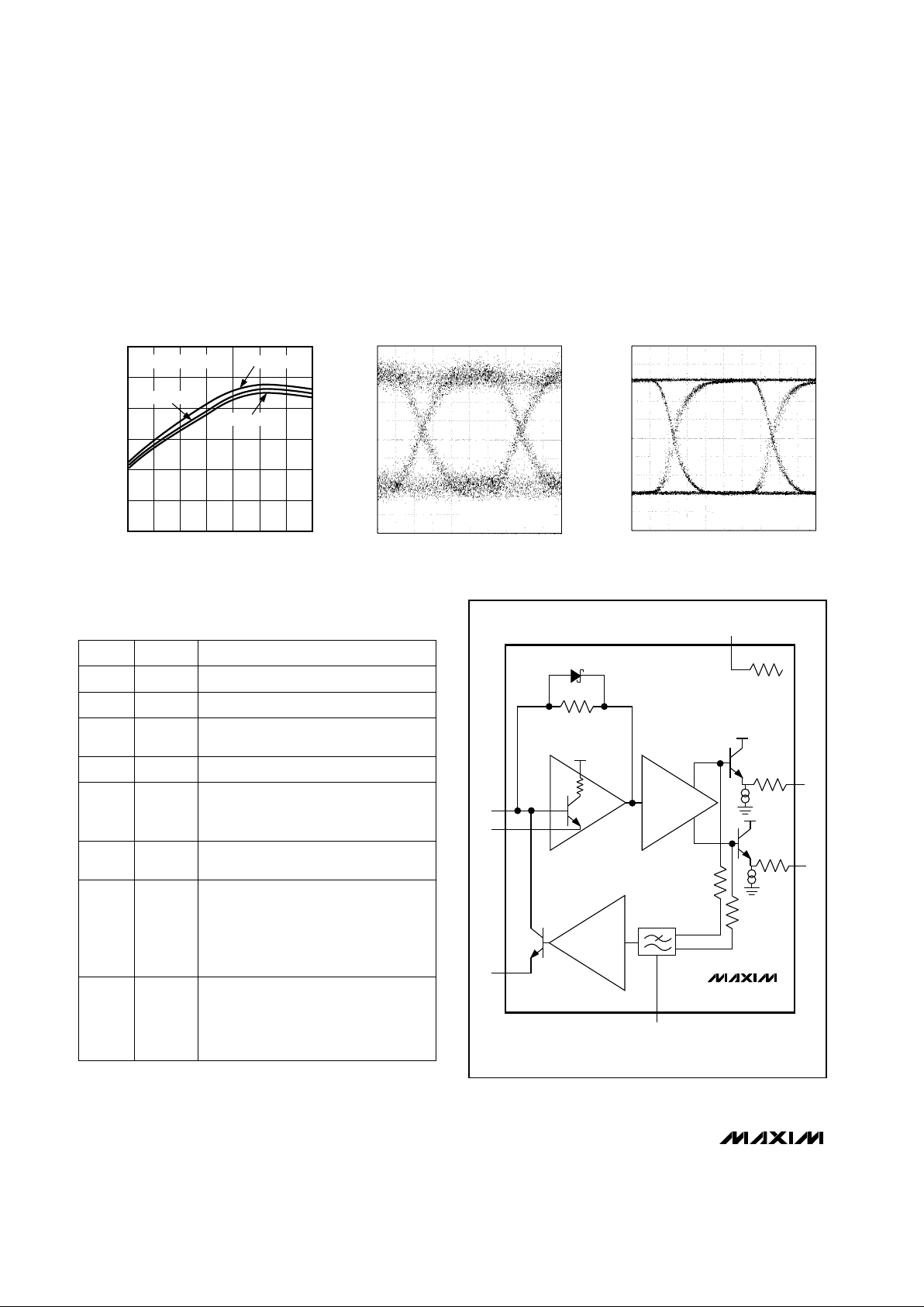
_____________________Pin Description
NAME FUNCTION
1
V
CC
+3.3V Supply Voltage
2 IN Signal Input
PIN
3, 4
INREF1,
INREF2
Input References 1 and 2. Connect to
photodetector AC ground.
5 GND Ground
— FILT*
Filter Connection. Provides positive
bias for photodiode through a 1kΩ
resistor to VCC. See
Step 3:
Designing Filters
. (This pad is acces-
sible on the die only.)
8 COMP
External Compensation Capacitor for
DC cancellation loop. Connect 400pF
or more from COMP to GND for normal operation. Connect COMP directly
to GND to disable the DC cancellation
loop.
7 OUT-
Inverting Voltage Output. Current flowing into IN causes V
OUT-
to decrease.
6 OUT+
Noninverting Voltage Output. Current
flowing into IN causes V
OUT+
to
increase.
* MAX3664E/D (die) only.
Figure 1. Functional Diagram
 Loading...