

Page 1
General Description
The MAX3656 is a burst-mode laser driver that operates at data rates from 155Mbps up to 2.5Gbps. The
laser driver accepts either positive-referenced emittercoupled logic (PECL) or current-mode logic (CML) data
inputs and provides bias and modulation current for the
laser diode. The device can switch the laser diode from
a completely dark (off) condition to a full (on) condition
(with proper bias and modulation currents) in less than
2ns. The MAX3656 incorporates DC-coupling between
laser driver and laser diode and operates with a singlesupply voltage as low as +3.0V.
A digital automatic power-control (APC) loop is provided
to maintain the average optical power over the full temperature range and lifetime. The APC loop is functional
for a minimum burst on-time of 576ns and minimum
burst off-time of 96ns, with no limit on the maximum
burst on- or off-time. A fail monitor is provided to indicate when the APC loop can no longer maintain the
average power. The MAX3656 can be configured for
nonburst-mode applications (continuous mode) by connecting burst enable (BEN) high. For power saving, the
MAX3656 provides enabling and disabling functionality.
The modulation current can be set from 10mA to 85mA
and the bias current can be set from 1mA to 70mA.
The MAX3656 is packaged in a small, 24-pin, 4mm
✕
4mm thin QFN package and consumes only 132mW
(typ), excluding bias and modulation currents.
Applications
Fiber-to-the-Home (FTTH) and Fiber-to-theBusiness (FTTB) Broadband Access Systems
Passive Optical Network (PON) Transmitters
APON, EPON, and GPON Upstream Transmitters
Features
♦ Multirate Operation from 155Mbps to 2.5Gbps
♦ Burst Enable/Disable Delay <2ns
♦ Burst On-Time of 576ns to Infinity
♦ Infinite Bias-Current Hold Time Between Bursts
♦ DC-Coupled Operation with Single +3.3V Power
Supply
♦ 40mA Typical Supply Current
♦ Programmable Bias Current from 1mA to 70mA
♦ Programmable Modulation Current from 10mA
to 85mA
♦ Automatic Average Power Control with Failure
Monitor (No C
APC
Capacitor Needed)
♦ APC Loop Initialization ≤3 Bursts
MAX3656
155Mbps to 2.5Gbps Burst-Mode
Laser Driver
________________________________________________________________ Maxim Integrated Products 1
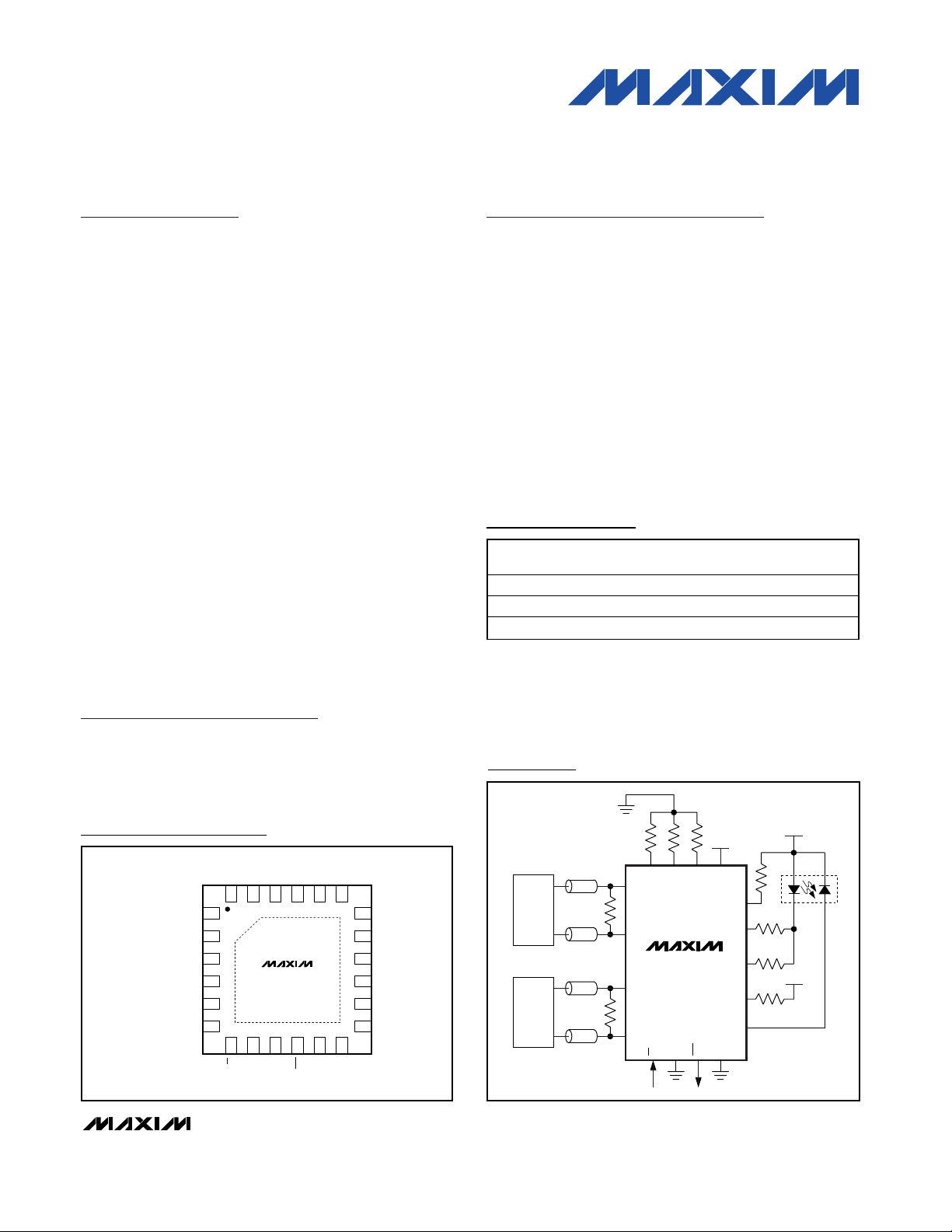
Pin Configuration
SERIAL
DATA
SOURCE
IN+
IN-
BEN+
BEN-
V
CC
100Ω
100Ω
OUT-
APCSET
MODSET
BIASMAX
EN
GND
FAIL
LONGB
OUT+
BIAS+
BIAS-
MD
MAX3656
BURST
CONTROL
V
CC
V
CC
V
CC
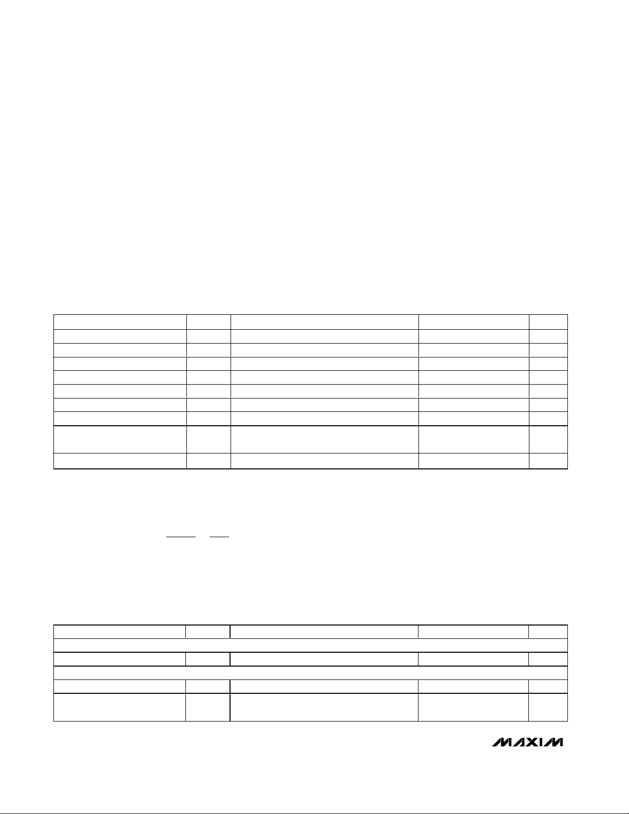
Typical Application Circuit
19-2790; Rev 2; 10/04
For pricing, delivery, and ordering information, please contact Maxim/Dallas Direct! at
1-888-629-4642, or visit Maxim’s website at www.maxim-ic.com.
+ Denotes lead-free package.
*Dice are designed to operate from T
J
= -40°C to +120°C, but
are only tested and guaranteed at T
A
= +25°C.
**EP = Exposed pad.
Ordering Information
Functional Diagram appears at end of data sheet.
PART TEMP RANGE PIN-PACKAGE
MAX3656E/D — Dice* —
MAX3656ETG -40°C to +85°C 24 Thin QFN-EP** T2444-1
MAX3656ETG+ -40°C to +85°C 24 Thin QFN-EP** T2444-1
PKG
CODE
TOP VIEW
V
CC
IN+
IN-
V
CC
BEN+
BEN-
**EXPOSED PAD IS CONNECTED TO GND
MODSET
APCSET
1
2
3
4
5
6
MAX3656
7891011 12
CC
EN
V
GND
THIN QFN
GND
MD
VCCBIASMAX
192021222324
18
V
CC
17
OUT-
16
LONGB
OUT+
V
15
CC
14
BIAS+
BIAS-
13
FAIL
GND
Page 2
MAX3656
155Mbps to 2.5Gbps Burst-Mode
Laser Driver
2 _______________________________________________________________________________________
ABSOLUTE MAXIMUM RATINGS
Stresses beyond those listed under “Absolute Maximum Ratings” may cause permanent damage to the device. These are stress ratings only, and functional
operation of the device at these or any other conditions beyond those indicated in the operational sections of the specifications is not implied. Exposure to
absolute maximum rating conditions for extended periods may affect device reliability.
Supply Voltage, VCC..............................................-0.5V to +6.0V
Current into BIAS+, BIAS-, OUT+, OUT- ........-20mA to +150mA
Current into MD.................................................... -5mA to +5mA
Current into FAIL ...............................................-10mA to +10mA
Voltage at IN+, IN-, BEN+, BEN-, EN,
LONGB...................................................-0.5V to (V
CC
+ 0.5V)
Voltage at MODSET, APCSET, BIASMAX .............-0.5V to +3.0V
Voltage at OUT+, OUT-.............................+0.5V to (V
CC
+ 1.5V)
Voltage at BIAS+, BIAS-............................+0.5V to (V
CC
+ 0.5V)
Continuous Power Dissipation (T
A
= +85°C)
24-Lead Thin QFN-EP
(derate 27.8mW/°C above +85°C).............................1805mW
Operating Ambient Temperature
Range (T
A
).......................................................-40°C to +85°C
Operating Junction Temperature
Range (T
J
) .....................................................-55°C to +150°C
Storage Ambient Temperature
Range (T
STG
).................................................-55°C to +150°C
Processing Temperature (die) .........................................+400°C
Lead Temperature (soldering,10s) ..................................+300°C
OPERATING CONDITIONS
Note 1: Larger MD capacitance increases the minimum burst on-time.
Note 2: Laser-to-monitor gain equals the laser slope efficiency multiplied by the photodiode responsivity multiplied by the losses due
to laser-to-monitor diode coupling (A
LMD
= η
LASER
✕ ρ
MONITORDIODE
✕ L
LASER-TO-MONITORDIODE
).
where L = laser-to-monitor diode coupling loss. A
LMD
can also be calculated by:
where I
MD
, I
MOD
, and re(extinction ratio) are set externally.
Note 3: Operation outside this range degrades APC loop performance.
ELECTRICAL CHARACTERISTICS
(Typical values are at VCC= +3.3V, I
BIAS
= 20mA, I
MOD
= 25mA, extinction ratio = 10dB, and TA= +25°C, unless otherwise noted.)
Supply Voltage V
Supply Turn-On Time 10% to 90% 0.001 10 ms
Ambient Temperature -40 +85 °C
Data Mark Density Average 50 %
Consecutive Identical Digits CID 80 Bits
Data Rate 155 2500 Mbps
Monitor Diode Capacitance C
Laser-to-Monitor Diode Gain A
Extinction Ratio r
PARAMETER SYMBOL CONDITIONS MIN TYP MAX UNITS
CC
For minimum burst on-time (Note 1) 15 pF
MD
∆ ( m oni tor cur r ent) /∆ ( l aser cur r ent ( ab ove I
LMD
( N otes 2, 3)
10 log (P1/P0) (Note 3) 8.2 12.0 dB
e
A
=
LMD
×
I
MOD
MD
e
rI
e
−2I r I
+
T H
3.0 3.3 3.6 V
) )
0.005 0.050 A/A
POWER SUPPLY
Power-Supply Current I
INPUT SPECIFICATIONS
Differential Input Voltage V
Common-Mode Input Voltage V
PARAMETER SYMBOL CONDITIONS MIN TYP MAX UNITS
, V
I N
CC
CM
(Note 1) 40 70 mA
B E N
0.2 1.6 V
VCC -
1.49
VCC -
1.32
V
V
C C
IN
P-P
-
/4
V
Page 3
MAX3656
155Mbps to 2.5Gbps Burst-Mode
Laser Driver
_______________________________________________________________________________________ 3
ELECTRICAL CHARACTERISTICS (continued)
(Typical values are at VCC= +3.3V, I
BIAS
= 20mA, I
MOD
= 25mA, extinction ratio = 10dB, and TA= +25°C, unless otherwise noted.)
PARAMETER SYMBOL CONDITIONS MIN TYP MAX UNITS
Single-Ended Input Voltage
EN Input High Voltage V
EN Input Low Voltage V
FAIL Output High Voltage V
FAIL Output Low Voltage V
V
BEN+
V
BEN-
,
IH
IL
S our ci ng 50µA, VCC = 3.0V 2.4 V
OH
S i nki ng 100µA, V CC = 3.6V 0.4 V
OL
0.8 V
2.0 V
0.8 V
BIAS GENERATOR
Bias-On Current Range I
Bias-Off Current Range I
BIAS
BIAS-OFF
Bias-Current Temperature
Stability
Bias-Current Absolute Accuracy APC open-loop I
Voltage at BIAS pin ≥ 0.6V 1 70 mA
EN = high or BEN = low, V
I
APC open loop
BIAS
I
BIAS
> 20mA (Note 3) -15 +15 %
BIAS
≤ 2.6V (Note 2) 5 100 µA
BIAS
= 70mA 148
= 15mA 98
ppm/°C
BIAS M AX C ur r ent- S etti ng Rang e1570mA
APC LOOP
MD Reverse-Bias Voltage V
MD Bias-Setting Stability
(Note 4)
MD Bias-Setting Accuracy
(Note 3)
MD DC-Current Range I
MD
With respect to V
CC
1.6 V
IMD = 50µA -750 +750
= 1500µA -480 +480
I
MD
IMD = 50µA -25 +25
= 1500µA -15 +15
I
MD
Average current into MD pin 50 1500 µA
MD
ppm/°C
%
Case 1 (Note 5) (LONGB = 0) 12
APC Loop Initialization Time
(Note 4)
t
INIT
Case 2 (Note 6) (LONGB = 0) 2.12
µs
Case 3 (Note 7) (LONGB = 0) 1.60 1.92
LASER MODULATOR
Modulation ON Current Range I
Modulation OFF Current I
MOD
MOD-OFF
Data rate ≤1.25Gbps 10 85
Data rate >1.25Gbps 10 60
mA
EN = high or BEN = low, IN = low (Note 2) 16 150 µA
Modulation-Current Stability (Note 13) -480 +480 ppm/°C
Modulation-Current Absolute
Accuracy
Instantaneous Voltage at
Modulator Output (OUT+)
Modulation-Current Rise Time t
Modulation-Current Fall Time t
R
F
> 15mA (Note 3) -15 +15 %
I
MOD
10mA ≤ I
60mA ≤ I
10mA ≤ I
10mA ≤ I
< 60mA 0.6
MOD
≤ 85mA 0.75
MOD
≤ 85mA (Notes 8, 13) 40 85 ps
MOD
≤ 85mA (Notes 8, 13) 40 85 ps
MOD
V
Output Over-/Undershoot 20 %
Deterministic Jitter
(Notes 9, 13)
DJ
155Mbps to 1.25Gbps, 10mA ≤ I
1.25Gbps to 2.5Gbps, 10mA ≤ I
Random Jitter RJ (Note 13) 0.8 1.4 ps
≤ 85mA 17 45
MOD
≤ 60mA 17 40
MOD
ps
P-P
RMS
Page 4
MAX3656
155Mbps to 2.5Gbps Burst-Mode
Laser Driver
4 _______________________________________________________________________________________
ELECTRICAL CHARACTERISTICS (continued)
(Typical values are at VCC= +3.3V, I
BIAS
= 20mA, I
MOD
= 25mA, extinction ratio = 10dB, and TA= +25°C, unless otherwise noted.)
Note 1: Excludes I
BIAS
and I
MOD
. Maximum value is specified at I
MOD
= 85mA, I
BIAS
= 70mA, and IMD= 1.5mA.
Note 2: For safety purposes, both the bias and modulation currents are switched off if any of the current set pins (BIASMAX, MODSET)
are grounded.
Note 3: Accuracy refers to part-to-part variation.
Note 4: APC loop initialization definitions:
I
BIAS
Error: I
BIAS
- I
BIASSET
, where I
BIAS
= the actual bias current and I
BIASSET
= the level of bias current set by the R
APCSET
resistor.
Initialization Case 1: Continuous Mode Power-Up. In this case, EN = low, BEN = high, and then V
CC
is ramped up from
0V to ≥3.0V.
Initialization Case 2: Chip-Enable Reset. In this case, 3.0V ≤ VCC≤ 3.6V, BEN = high, and then EN changes from high to low.
Initialization Case 3: Burst-Mode Startup. In this case, 3.0V ≤ V
CC
≤ 3.6V, EN = low, and then BEN changes from low to high.
Note 5: I
BIAS
error is less than 3.8mA (for an extinction ratio of 10dB and IMD= 1500µA) within 12µs from the time that VCC≥ 3.0V.
Note 6: I
BIAS
error is less than 3.8mA (for an extinction ratio of 10dB and IMD= 1500µA) within 2.1µs (typ) from the time that EN < 0.8V.
Note 7: I
BIAS
error must be less than 3.8mA (for an extinction ratio of 10dB and IMD= 1500µA) at or before the end of the third
burst following the transition of BEN from low to high. For the shortest burst on- and off-time (576ns and 96ns), this translates to 1.92µs from when BEN toggles from low to high for the first time after startup.
Note 8: Rise and fall times are measured as 20% to 80% of the output amplitude with a repeating 0000011111.
Note 9: Deterministic jitter is measured with a continuous data pattern (no bursting) of 2
7
- 1 PRBS + 80 consecutive ones + 27- 1
PRBS + 80 consecutive zeros.
Note 10: Measured electrically with a resistive load matched to the laser driver output.
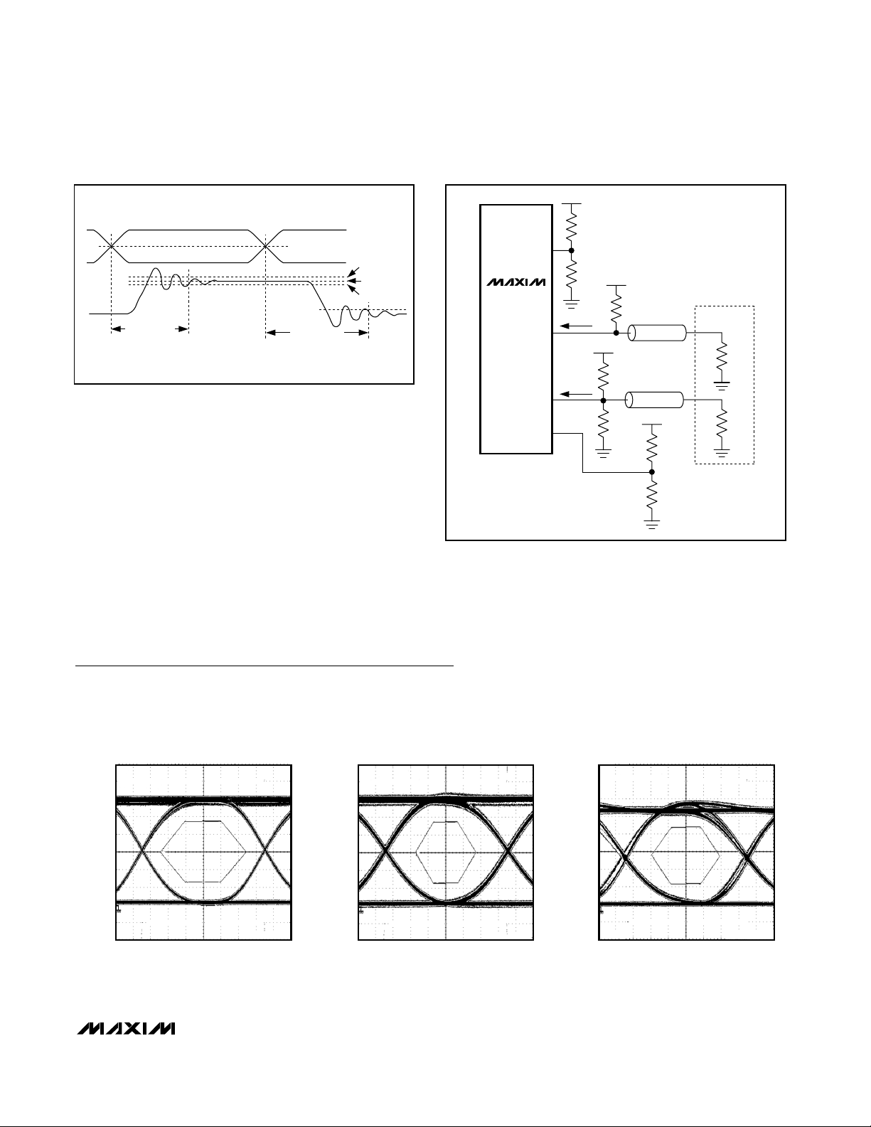
Note 11: Enable delay is measured between (1) the time at which the rising edge of the differential burst enable input signal reach-
es the midpoint of the voltage swing, and (2) the time at which the combined output currents (bias and modulation) reach
90% of the final level set by R
APCSET
, R
BIASMAX
, and R
MODSET
(after all transients such as overshoot, ringing, etc., have
settled to within 10% of their final values). See Figure 1. Measurement done for 10mA ≤ I
MOD
≤ 85mA and 4mA ≤ I
BIAS
≤
70mA.
Note 12: Disable delay is measured between (1) the time at which the falling edge of the differential burst enable input signal reaches
the midpoint of the voltage swing, and (2) the time at which the combined output currents (bias and modulation) fall below
10% of the bias on current (after transients have settled). See Figure 1. Measurement done for 10mA ≤ I
MOD
≤ 85mA and
4mA ≤ I
BIAS
≤ 70mA.
Note 13: Guaranteed by design and characterization.
BURST-MODE SPECIFICATIONS
Burst Enable Delay APC closed loop (Notes 10, 11, 13) 2.3 ns
Burst Disable Delay APC closed loop (Notes 10, 12, 13) 2.0 ns
PARAMETER SYMBOL CONDITIONS MIN TYP MAX UNITS
OPTICAL EVALUATION
Optical Eye Diagram Mask
Margin
B-ON
B-OFF
155Mbps 2881
622Mbps 720Burst On-Time (Note 13) t
1.25Gbps, 2.5Gbps 576
155Mbps 192
622Mbps 96Burst Off-Time (Note 13) t
1.25Gbps, 2.5Gbps 96
E xceLi g ht
S LT3120- D N
l aser d i od e
( or eq ui val ent)
155.52Mbps 42
622.08Mbps 30
1.25Gbps 23
2.48832Gbps 18
ns
ns
%
Page 5
MAX3656
155Mbps to 2.5Gbps Burst-Mode
Laser Driver
_______________________________________________________________________________________ 5
Figure 1. Enable and Disable Delay Times
Figure 2. Output Termination for Characterization
Typical Operating Characteristics
(TA = +25°C, unless otherwise noted.)
OPTICAL EYE DIAGRAM
(155.52Mbps, 117MHz FILTER,
PATTERN = PRBS 2
7
- 1 + 80 CID)
MAX3656 toc01
EXCELIGHT SLT3120-DN LASER
AVERAGE OPTICAL POWER = -4dBm
EXTINCTION RATIO = 15.2dB
MASK MARGIN = 42%
OPTICAL EYE DIAGRAM
(622.08Mbps, 467MHz FILTER,
PATTERN = PRBS 2
7
- 1 + 80 CID)
MAX3656 toc02
EXCELIGHT SLT3120-DN LASER
AVERAGE POWER = -4dBm
EXTINCTION RATIO = 15.1dB
MASK MARGIN = 30%
OPTICAL EYE DIAGRAM
(1.25Gbps, 933MHz FILTER,
PATTERN = PRBS 2
7
- 1 + 80 CID)
MAX3656 toc03
EXCELIGHT SLT3120-DN LASER
AVERAGE POWER = -3.5dBm
EXTINCTION RATIO = 14dB
MASK MARGIN = 23%
V
CC
BEN+
BEN-
I
BIAS
+
I
MOD
ENABLE DELAY
10% OF I
BEN ±MIDPOINT
BIAS
DISABLE DELAY
I
FINAL
I
I
FINAL
FINAL
× 110%
× 90%
22.1Ω
OUT-
49.9Ω
V
CC
MAX3656
22.1Ω
26.7Ω
121Ω
Z0 = 50Ω
= 50Ω
Z
0
V
CC
V
CC
OSCILLOSCOPE
26.7Ω
35.7Ω
OUT+
BIAS+
BIAS-
I
MOD
I
BIAS
50Ω
50Ω
Page 6

10
20
15
30
25
35
40
200 800 1000400 600 1200 1400 1600
DETERMINISTIC JITTER
vs. INPUT AMPLITUDE
MAX3656 toc07
INPUT AMPLITUDE (mV
P-P
)
DETERMINISTIC JITTER (ps
P-P
)
I
MOD
= 30mA
PATTERN = 2
7
- 1PRBS + 80 CID
DATA RATE = 2.5Gbps
0.5
0.7
0.6
0.9
0.8
1.1
1.0
1.2
1.4
1.3
1.5
10 30
402050 60 70 80
RANDOM JITTER vs. I
MOD
MAX3656 toc08
I
MOD
(mA)
RANDOM JITTER (ps
RMS
)
10,000
10
0.1 10 100
IMD vs. R
APCSET
100
1000
MAX3656 toc09
R
APCSET
(kΩ)
I
MD
(µA)
1
100
90
80
70
60
50
40
30
20
10
0
110100
I
MOD
vs. R
MODSET
MAX3656 toc10
R
MODSET
(kΩ)
I
MOD
(mA)
100
90
80
70
60
50
40
30
20
10
0
110100
I
BIASMAX
vs. R
BIASMAX
MAX3656 toc11
R
BIASMAX
(kΩ)
I
BIASMAX
(mA)
MAX3656
155Mbps to 2.5Gbps Burst-Mode
Laser Driver
6 _______________________________________________________________________________________
Typical Operating Characteristics (continued)
(TA = +25°C, unless otherwise noted.)
ELECTRICAL EYE DIAGRAM
(2.5Gbps, I
PATTERN = PRBS 2
MOD
100ps/div
= 30mA,
7
- 1 + 80 CID)
MAX3656 toc04
SUPPLY CURRENT vs. TEMPERATURE
(EXCLUDES I
80
75
70
65
60
55
50
45
SUPPLY CURRENT (mA)
40
35
30
-40 -20 -10-30 0 10 20 304050607080
BIAS, IMOD,
TEMPERATURE (°C)
15Ω LOAD)
MAX3656 toc05
DETERMINISTIC JITTER vs. I
40
DATA RATE = 2.5Gbps
PATTERN = 2
35
)
V
P-P
30
25
20
DETERMINISTIC JITTER (ps
15
10
10 30 4020 50 60 70 80
= 200mV
IN
7
- 1PRBS + 80 CID
P-P
I
(mA)
MOD
MOD
MAX3656 toc06
Page 7

MAX3656
155Mbps to 2.5Gbps Burst-Mode
Laser Driver
_______________________________________________________________________________________ 7
Typical Operating Characteristics (continued)
(TA = +25°C, unless otherwise noted.)
Pin Description
PIN NAME FUNCTION
1, 4, 9,
15, 18, 21
2 IN+ Noninverting Data Input with On-Chip Biasing
3 IN- Inverting Data Input with On-Chip Biasing
5 BEN+ Noninverting Burst-Enable Input with On-Chip Biasing
6 BEN- Inverting Burst-Enable Input with On-Chip Biasing
7 EN
8, 11, 19 GND Power-Supply Ground
10 FAIL TTL/CMOS Failure Output. Indicates APC failure when low.
12 LONGB TTL/CMOS Long Burst (See the Setting the LONGB Input Pin Section)
13 BIAS- Inverting Laser Bias-Current Output. Connect through 15Ω to VCC.
14 BIAS+
16 OUT+
17 OUT- Inverting Laser Modulation-Current Output. Connect through 15Ω to VCC.
20 MD
TIMING DIAGRAM, BURST ON
V
MOD+
V
BIAS+
BURST-ENABLE
SIGNAL
500ps/div
V
CC
Power-Supply Voltage
TTL/CMOS Enable Input. Low for normal operation. Float or pull high to disable laser bias and
modulation currents.
Noninverting Laser Bias-Current Output. Bias current flows into this pin when BEN is high. Minimize
capacitance on this pin.
Noninverting Laser Modulation-Current Output. Modulation current flows into this pin when BEN and IN
are high.
Monitor Diode Input. Connect this pin to the anode of the monitor diode. Leave floating for open-loop
operation. Minimize capacitance on this pin.
MAX3656 toc12
TIMING DIAGRAM, BURST OFF
BURST-DISABLE
SIGNAL
1ns/div
MAX3656 toc13
V
MOD+
V
BIAS+
Maximum Bias Current Set. A resistor connected from this pin to ground sets the maximum bias
22 BIASMAX
23 MODSET M od ul ati on C ur r ent S et. A r esi stor connected fr om thi s p i n to g r ound sets the d esi r ed m od ul ati on cur r ent.
24 APCSET
EP Exposed Pad Ground. This pad must be soldered to ground.
current. The bias current cannot exceed this level. The APC loop controls the bias current up to the
level of the BIASMAX. For APC open-loop operation, this pin sets the laser bias current.
Average Power Control Set. A resistor connected from this pin to ground sets the desired average
optical power. Connect a 50kΩ resistor to ground for APC open-loop operation.
Page 8

MAX3656
Detailed Description
The MAX3656 laser driver has three main parts: a highspeed modulator, a high-speed bias driver, and a laserbiasing block with automatic power control (see the
Functional Diagram). Both the bias and modulation output
stages are composed of differential pairs with programmable current sources. The circuit design is optimized for
high-speed, low-voltage (3.3V), DC-coupled operation.
The device is ideal for burst-mode operation with turn-on
and turn-off times less than 2ns. The MAX3656 can be
configured for nonburst-mode applications (continuous
mode) by connecting BEN high.
The MAX3656 modulation output is optimized for driving a 15Ω load. The modulation current can swing up
to 85mA for data rates less than or equal to 1.25Gbps
and up to 60mA for data rates greater than 1.25Gbps
when the laser is DC-coupled. To interface with the
laser diode, a damping resistor (RD) is required for
impedance matching. The combined resistance due to
the series damping resistor and the equivalent series
resistance (ESR) of the laser diode should be equal to
15Ω. The OUT- pin should be connected with a 15Ω
resistor to VCC. To reduce optical output aberrations
and duty-cycle distortion caused by laser diode parasitic inductance, an RC shunt network is necessary.
The currents in the BIAS output switch at high speeds
when bursting. Therefore, the BIAS+ pin should be connected directly through a resistor to the cathode of the
laser. The BIAS- pin should be connected to V
CC
through a 15Ω resistor.
Automatic Power Control
To maintain constant average optical power, the
MAX3656 incorporates a digital automatic power-control (APC) loop to compensate for the changes in laser
threshold current over temperature and lifetime. A
back-facet photodiode mounted in the laser package
converts the optical power into a photocurrent. The
APC loop adjusts the laser bias current so the monitor
current is matched to a reference current set by R
APCSET
.
At startup, the APC loop traverses through a pseudobinary search algorithm to set the proper monitor current
that translates to the proper bias current. When BEN is
high, the APC loop maintains constant optical power by
digitally controlling the bias current. When BEN is low,
the APC loop digitally stores the bias current value of the
previous burst. The APC loop is reset in two ways, either
power cycling or toggling the EN pin.
An external resistor (R
BIASMAX
) sets the maximum allowable bias current during closed-loop operation and sets
the bias current during open-loop operation. An APC fail-
ure flag (FAIL) is set low during initialization and when
the bias current cannot be adjusted to achieve the
desired average optical power.
APC closed-loop operation requires that the user set
three currents with external resistors connected between
GND, BIASMAX, MODSET, and APCSET pins. Detailed
guidelines for these resistor settings are described in the
Design Procedure section.
If necessary, the MAX3656 is fully operational without
APC. To operate the MAX3656 open loop, connect a
50kΩ resistor from APCSET to ground and leave the
MD pin unconnected. In this case, two external resistors connected from BIASMAX and MODSET to GND
directly set the laser current.
APC Failure Monitor
The MAX3656 provides an APC failure monitor (TTL) to
indicate an APC loop-tracking failure. FAIL is set low
when the APC loop cannot adjust the bias current to
maintain the desired monitor current. For example, the
laser diode requires more bias current (to maintain a
constant optical output) than maximum bias current set
by R
BIASMAX
. The bias current is limited and FAIL is
asserted. In an alternate example, assume that a circuit
failure causes the cathode of the laser diode to be shorted to GND, thereby causing an uncontrolled high optical
output. In this case, the APC loop cannot decrease the
user current, and FAIL is asserted. FAIL is also set low
during initialization.
Slow-Start
For safety reasons, at initial power-up or after toggling
EN, the MAX3656 incorporates a slow-start circuit that
provides a typical delay of 450ns during the beginning
of APC loop initialization.
Enable Control
The MAX3656 features a chip-enable function. When
EN is high, the bias and modulation currents are off and
the digital state of the APC loop is reset. When EN is
toggled from a high to a low, the APC loop begins initialization. The initialization time is typically 2.1µs
(LONGB = low) and 3.72µs (LONGB = high).
APC Loop Initialization
The digital APC loop is reset whenever the power is
turned off and/or the EN input is driven high. When
power is turned on or when EN is toggled low, the APC
loop automatically performs an initialization routine that
quickly adjusts the bias current from its reset level to its
initialized level. The initialized bias current level is
defined to be within 3.8mA of the final bias current level
set by the APCSET resistor. Once initialized, the APC
155Mbps to 2.5Gbps Burst-Mode
Laser Driver
8 _______________________________________________________________________________________
Page 9

loop enters its fine-adjustment mode of operation and
adjusts the bias current to match the level set by the
APCSET resistor. There are three different cases in
which the APC loop starts initialization, and each has a
unique initialization time. These cases are defined
as follows:
• Continuous-Mode Power-Up
In continuous-mode power-up, the chip is enabled
(EN = low) and the burst-enable input is high (BEN =
high) when power is applied to the laser driver. APC
loop initialization begins when the power-supply voltage rises above the minimum specified limit of +3.0V.
The BEN input remains high indefinitely and the laser
driver operates in continuous (nonbursting) mode. In
this case, the initialization time is 12µs (typ).
• Chip-Enable Reset
In chip-enable reset, the power-supply voltage is
within the specified limits and BEN is high. The
chip-enable input (EN) is initially high (chip disabled and APC loop reset), and then it is driven low
(chip-enabled). In this case, APC loop initialization
begins when the voltage at EN drops below the
specified EN input low voltage of 0.8V. After initialization begins, the laser driver can be operating in
burst mode (BEN toggling high and low) or continuous mode (BEN = high). In this case, the initialization time is 2.1µs (typ).
• Burst-Mode Startup
In burst-mode startup, the power-supply voltage is
within the specified limits and the chip is enabled
(EN = low). The burst-enable input is low (BEN =
low) and has not been in the high state since the
APC loop was reset. APC loop initialization begins
when the BEN input is driven high. After initialization
begins, the laser driver can be operating in burst
mode (BEN toggling high and low) or continuous
mode (BEN = high). In this case, the initialization
time is 1.6µs (typ).
In each of the three cases listed, initialization is complete
within three bursts (bursts must comply with specified
burst on- and burst off-time) or the time specified in the
Electrical Characteristics table, whichever comes first.
Burst-Mode Operation
The bias and modulation outputs (BIAS+ and OUT+)
can be switched on and off quickly using the differential
burst-enable inputs (BEN+ and BEN-). Once the APC
loop has initialized, the bias and modulation outputs are
switched on when BEN+ = high and BEN- = low and are
switched off when BEN+ = low and BEN- = high.
When BEN is switched on, the laser driver sinks the bias
and modulation currents set by the APCSET, BIASMAX,
and MODSET resistors within the maximum BEN delay
time of 2.3ns. For stable APC loop operation, the minimum burst length is limited to the burst on-time listed in
the Electrical Characteristics table. The maximum burst-
on time is unlimited.
When BEN is switched off, the bias and modulation currents fall below the specified bias-off and modulationoff currents within the maximum burst disable delay
time of 2.0ns. For stable APC loop operation, the minimum burst off-time is limited to the value listed in the
Electrical Characteristics table. The maximum burst offtime is unlimited.
Short-Circuit Protection
The MAX3656 provides short-circuit protection for the
modulation and bias-current sources. If BIASMAX or
MODSET is shorted to ground, the bias and modulation
outputs are turned off.
Design Procedure
When designing a laser transmitter, the optical output is
usually expressed in terms of average power and
extinction ratio. Table 1 shows the relationships helpful
in converting between the optical average power and
the modulation current. These relationships are valid if
the mark density and duty cycle of the optical waveform are 50%.
Programming the Modulation Current
For a given laser power (P
AVG
), slope efficiency (η),
and extinction ratio (re), the modulation current can be
calculated using Table 1. See the I
MOD
vs. R
MODSET
graph in the Typical Operating Characteristics, and
select the value of R
MODSET
that corresponds to the
required current at +25°C.
MAX3656
155Mbps to 2.5Gbps Burst-Mode
Laser Driver
_______________________________________________________________________________________ 9
Table 1. Optical Power Definition
PARAMETER SYMBOL RELATION
Average power P
Extinction ratio r
Optical power high P
Optical power low P
Optical amplitude P
Laser slope
efficiency
Modulation current I
Laser-to-monitor
diode gain
AVGPAVG
e
1
0
P-P
ηη = P
MODIMOD
A
LMD
= (P0 + P1) / 2
re = P1 / P
P1 = 2P
P0 = 2P
P
P-P
(2 x I
(r
e
= P1 - P
P-P
= P
MD
+ 1))
0
× re / (re + 1)
AVG
/ (re + 1)
AVG
0
/ I
MOD
/ η
P-P
/ I
)((re - 1) /
MOD
Page 10

MAX3656
Programming the Bias Current
When the MAX3656 is used in open-loop operation, the
R
BIASMAX
resistor determines the bias current. To
select this resistor, determine the required bias current.
See the I
BIASMAX
vs. R
BIASMAX
graph in the Typical
Operating Characteristics, and select the value of
R
BIASMAX
that corresponds to the required current. For
open-loop operation, connect a 50kΩ resistor from
R
APCSET
to GND, and leave the MD pin open.
When using the MAX3656 in closed-loop operation, the
R
BIASMAX
resistor sets the maximum bias current available to the laser diode over temperature and lifetime.
The APC loop can subtract from this maximum value,
but cannot add to it. See the I
BIASMAX
vs. R
BIASMAX
graph in the Typical Operating Characteristics and
select the value of R
BIASMAX
that corresponds to the
end-of-life bias current at +85°C.
Programming the APC Loop
When using the MAX3656’s APC feature, program the
average optical power by adjusting the APCSET resistor. To select this resistor, determine the desired monitor current to be maintained over temperature and
lifetime. See the IMDvs. R
APCSET
graph in the Typical
Operating Characteristics and select the value of
R
APCSET
that corresponds to the required current.
Setting the LONGB Input Pin
Set the LONGB pin according to Table 2 to optimize
APC loop operation.
Interfacing with Laser Diodes
To minimize optical output aberrations caused by signal reflections at the electrical interface to the laser
diode, a series-damping resistor (RD) is required (see
the Functional Diagram). Additionally, the MAX3656
outputs are optimized for a 15Ω load. Therefore, the
series combination of RDand RL(where RLrepresents
the laser-diode resistance) should equal 15Ω. Typical
values for RDare 8Ω to 13Ω. For best performance, a
bypass capacitor (0.01µF typical) should be placed as
close as possible to the anode of the laser diode. An
RC shunt network between the OUT+ pin and ground
helps minimize optical output aberrations. Starting values for most coaxial lasers are R = 56Ω in series with C
= 10pF. Adjust these values experimentally until the
optical output waveform is optimized (refer to
Application Note HFAN 3.0: Interfacing Maxim’s Laser
Drivers with Laser Diodes).
Input Termination Requirements
The MAX3656 data and BEN inputs are internally biased.
Although the inputs are compatible with LVPECL signals,
it is not necessary to drive the MAX3656 with a standard
LVPECL signal. While DC-coupled, the MAX3656 operates properly as long as the specified common-mode
voltage and differential voltage swings are met.
Because of the on-chip biasing network (Figure 3), the
MAX3656 inputs self-bias to the proper operating point
to accommodate AC-coupling.
See Figures 4 and 5 for connecting to PECL or CML
data outputs.
155Mbps to 2.5Gbps Burst-Mode
Laser Driver
10 ______________________________________________________________________________________
Table 2. Setting the LONGB Input Pin
Figure 3. MAX3656 Internal Biasing
LONGB CONDITION
0 Burst on-time ≤1.2µs
0 or 1
1 Data rates of 155Mbps
Burst on-time >1.2µs or
continuous mode operation
V
V
CC
V
CC
IN+
V
IN-
V
BEN+
V
BEN-
5kΩ
CC
5kΩ
CC
5kΩ
CC
5kΩ
16kΩ
24kΩ
V
CC
16kΩ
24kΩ
CC
MAX3656
V
CC
Page 11

Design Example
Select Laser
Select a communication-grade laser for the proper data
rate. Assume the laser output average power is P
AVG
=
0dBm, the operating temperature is -40°C to +85°C
,
and the laser diode has the following characteristics:
wavelength: λ = 1.3µm, threshold current: ITH= 22mA
at +25°C, threshold temperature coefficient: βTH=
1.3%/°C, laser-to-monitor transfer: ρ
MON
= 0.2A/W
(ρ
MON
= ρ
MONITORDIODE
x L
LASER-TO-MONITORDIODE)
,
and laser slope efficiency: η = 0.05mW/mA at +25°C.
Determining R
APCSET
The desired monitor diode current is estimated by IMD=
P
AVG
✕
ρ
MON
= 200µA. The IMDvs. R
APCSET
graph in the
Typical Operating Characteristics shows R
APCSET
at 12kΩ.
Determining R
MODSET
Assuming re= 10 and an average power of 0dBm (1mW),
the peak-to-peak optical power P
P-P
= 1.64mW (Table 1).
The required modulation current is 1.64(mW)/0.05(mW/mA)
= 32.8mA. The I
MOD
vs. R
MODSET
graph in the Typical
Operating Characteristics shows R
MODSET
at 9kΩ.
Determining R
BIASMAX
Determine the maximum threshold current (I
TH(MAX)
) at
TA= +85°C and end of life. Assuming (I
TH(MAX)
) =
50mA, the maximum bias current should be:
I
BIASMAX
= I
TH(MAX)
In this example, I
BIASMAX
= 50mA. The I
BIASMAX
vs. R
BIASMAX
graph in the Typical Operating Charact-
eristics shows R
BIASMAX
at 8kΩ.
MAX3656
155Mbps to 2.5Gbps Burst-Mode
Laser Driver
______________________________________________________________________________________ 11
Figure 4. Connecting to PECL Outputs
Figure 5. Connecting to CML Outputs
Figure 6. Single-Ended Biasing for Burst Enable
V
CC
130Ω
ZO = 50Ω
ZO = 50Ω
82Ω
V
IN+
CC
MAX3656
130Ω
IN-
ZO = 50Ω
ZO = 50Ω
ZO = 50Ω
ZO = 50Ω
100Ω
100Ω
IN+
IN-
BEN+
BEN-
MAX3656
82Ω
V
CC
130Ω
ZO = 50Ω
82Ω
V
CC
130Ω
ZO = 50Ω
82Ω
BEN+
BEN-
V
+ (100mV to 800mV)
CMBEN
V
CMBEN
- (100mV to 800mV)
V
CMBEN
V
CMBEN
= +2.0V
3.3V
R
= 1.65kΩ
1
= 2.54kΩ
R
2
IN+
IN-
BEN+
BEN-
MAX3656
Page 12

MAX3656
Applications Information
Running Burst Enable Single-Ended
With PECL signal levels, for single-ended operation of
burst enable, connect the BEN+ to the burst-enable control. Connect a resistor (R1) from VCCto BEN- and resistor (R2) from BEN- to ground. The parallel combination of
R1and R2should be less than 1kΩ. Choose the values
of R1and R2to set the common-mode voltage in the
range defined in the Electrical Characteristics table (see
Figure 6).
With LVTTL or LVCMOS signal levels, for single-ended
operation of burst enable connect a 3kΩ (R4) resistor
from the burst-enable signal to BEN+. Connect a 5kΩ
(R3) resistor from VCCto BEN+. Connect a 5kΩ resistor
(R5) from VCCto BEN- and a 9kΩ resistor (R6) from BENto ground. For typical LVTTL or LVCMOS specifications of
VCCto 2.0V for a high and 0.8V to 0V for a low, the LVTTL
or LVCMOS sources a maximum of 75µA and sinks a
maximum of 500µA. See Figure 7 for setting up the single-ended LVTTL or LVCMOS biasing for burst enable.
Burst Enable Delay
For some lasers, replacing the 15Ω resistors connected
from OUT- and BIAS- to VCCwith surface-mount signal
diodes can reduce burst-enable delay.
Wire-Bonding Die
For high-current density and reliable operation, the
MAX3656 uses gold metalization. Make connections to
the die with gold wire only, using ball-bonding techniques. Die-pad size is 4.03 mils (102.4µm) square, and
die size is 98 mils ✕65 mils (2489.2µm ✕1651µm).
Layout Considerations
To minimize inductance, keep the connections between
the MAX3656 output pins and laser diode as close as
possible. Optimize the laser diode performance by placing a bypass capacitor as close as possible to the laser
anode. Take extra care to minimize stray parasitic capacitance on the BIAS and MD pins. Use good high-frequency layout techniques and multilayer boards with
uninterrupted ground planes to minimize EMI and
crosstalk.
155Mbps to 2.5Gbps Burst-Mode
Laser Driver
12 ______________________________________________________________________________________
Table 3. Pad Locations
Figure 7. Single-Ended LVTTL or LVCMOS Biasing for Burst
Enable
IN+
V
CC
LVTTL OR LVCMOS HIGH
LVTTL OR LVCMOS LOW
R3 = 5kΩ
= 3kΩ
R
4
R5 = 5kΩ
= 9kΩ
R
6
IN-
BEN+
V
CC
BEN-
MAX3656
PAD NAME COORDINATES (microns)
1VCC51.2 1146.0
2 IN+ 51.2 1003.2
3 IN- 51.2 856.2
4VCC51.2 709.2
5 BEN+ 51.2 198.2
6 BEN- 51.2 51.2
7 GND 142.2 -111.2
8 EN 282.2 -111.2
9 GND 423.6 -111.2
10 V
11 FAIL 1569.6 -111.2
12 GND 1738.2 -111.2
13 LONGB 1881.0 -111.2
14 GND 2023.8 -111.2
15 BIAS- 2257.6 87.6
16 BIAS+ 2257.6 236.0
17 V
18 OUT+ 2257.6 626.6
19 OUT+ 2257.6 768.0
20 OUT- 2257.6 931.8
21 OUT- 2257.6 1073.2
22 V
23 GND 2039.2 1242.6
24 MD 1893.6 1242.6
25 GND 1749.4 1242.6
26 V
27 GND 1461.0 1242.6
28 BIASMAX 700.8 1242.6
29 MODSET 555.2 1242.6
30 APCSET 412.4 1242.6
31 GND 262.6 1242.6
CC
CC
CC
CC
608.4 -111.2
2257.6 453.0
2257.6 1217.4
1603.8 1242.6
Page 13
Laser Safety and IEC825
Using the MAX3656 laser driver alone does not ensure
that a transmitter design is compliant with IEC825. The
entire transmitter circuit and component selections must
be considered. Each user must determine the level of
fault tolerance required by the application, recognizing
that Maxim products are neither designed nor authorized
for use as components in systems intended for surgical
implant into the body, for applications intended to support
or sustain life, or for any other application in which the failure of a Maxim product could create a situation where
personal injury or death can occur.
MAX3656
155Mbps to 2.5Gbps Burst-Mode
Laser Driver
______________________________________________________________________________________ 13
Functional Diagram
MAX3656
IN+
V
CC
I
MOD
OUT+
OUT-
R
COMP
C
R
COMP
D
V
CC
IN-
BEN+
BEN-
R
MODSET
APC
DAC DSP ASP
R
BIASMAX
EN FAIL
LONGB
I
BIAS
R
APCSET
BIAS+
BIAS-
MD
V
CC
Page 14
MAX3656
155Mbps to 2.5Gbps Burst-Mode
Laser Driver
14 ______________________________________________________________________________________
Chip Topography
Chip Information
TRANSISTOR COUNT: 8153
SUBSTRATE: Electrically isolated
DIE SIZE: 2489.2µm X 1651µm
DIE THICKNESS: 12 mils
PROCESS: SiGe bipolar
MODSET
V
GND
V
CC
APCSET
BIASMAX
GND
GND
CC
MD
GND
V
CC
(0,0)
V
BEN+
BEN-
IN+
IN-
CC
GND
MAX3656
GND V
CC
0.098"
(2.489mm)
OUT-
OUT+
0.065"
(1.651mm)
V
CC
BIAS+
BIAS-
FAILEN
GND
LONGB
GND
Page 15

MAX3656
155Mbps to 2.5Gbps Burst-Mode
Laser Driver
______________________________________________________________________________________ 15
Package Information
(The package drawing(s) in this data sheet may not reflect the most current specifications. For the latest package outline information,
go to www.maxim-ic.com/packages
.)
24L QFN THIN.EPS
PACKAGE OUTLINE,
12, 16, 20, 24, 28L THIN QFN, 4x4x0.8mm
21-0139
1
D
2
Page 16
MAX3656
155Mbps to 2.5Gbps Burst-Mode
Laser Driver
Package Information (continued)
(The package drawing(s) in this data sheet may not reflect the most current specifications. For the latest package outline information,
go to www.maxim-ic.com/packages
.)
Maxim cannot assume responsibility for use of any circuitry other than circuitry entirely embodied in a Maxim product. No circuit patent licenses are
implied. Maxim reserves the right to change the circuitry and specifications without notice at any time.
16 ____________________Maxim Integrated Products, 120 San Gabriel Drive, Sunnyvale, CA 94086 408-737-7600
© 2005 Maxim Integrated Products Printed USA is a registered trademark of Maxim Integrated Products, Inc.
PACKAGE OUTLINE,
12, 16, 20, 24, 28L THIN QFN, 4x4x0.8mm
21-0139
2
D
2
 Loading...