

Page 1
General Description
The MAX361/MAX362 are precision, quad, single-pole
single-throw (SPST) analog switches. The MAX361 has four
normally closed (NC) switches, and the MAX362 has four
normally open (NO) switches. Both parts offer low channel
on-resistance (less than 85Ω), guaranteed to match within
3Ω between channels and to remain flat over the analog
signal range (∆9Ω max). Both parts also offer low leakage
(less than 500pA at +25°C and less than 4nA at +85°C) and
fast switching (turn-on time less than 250ns and turn-off time
less than 170ns).
The MAX361/MAX362 are fabricated with Maxim’s new
improved 44V silicon-gate process. Design improvements guarantee extremely low charge injection
(10pC), low power consumption (35µW), and electrostatic discharge (ESD) greater than 2000V. The 44V
maximum breakdown voltage allows rail-to-rail analog
signal handling capability.
These monolithic switches operate with a single positive
supply (+10V to +30V) or with split supplies (±4.5V to ±20V)
while retaining CMOS-logic input compatibility and fast
switching. CMOS inputs provide reduced input loading.
________________________Applications
Sample-and-Hold Circuits
Guidance and Control Systems
Heads-Up Displays
Test Equipment
Communications Systems
Battery-Operated Systems
PBX, PABX
____________________________Features
♦ Low On Resistance: < 45Ω Typical (85Ω Max)
♦ Guaranteed Matched On-Resistance Between Channels: < 2Ω
♦ Guaranteed Flat On-Resistance over Analog Signal
Range: ∆9Ω Max
♦ Guaranteed Charge Injection: < 10pC
♦ Guaranteed Off-Channel Leakage: <4nA at +85°C
♦ ESD Guaranteed > 2000V per Method 3015.7
♦ Single-Supply Operation (+10V to +30V)
Bipolar-Supply Operation (±4.5V to ±20V)
♦ TTL-/CMOS-Logic Compatible
♦ Rail-to-Rail Analog Signal Handling Capability
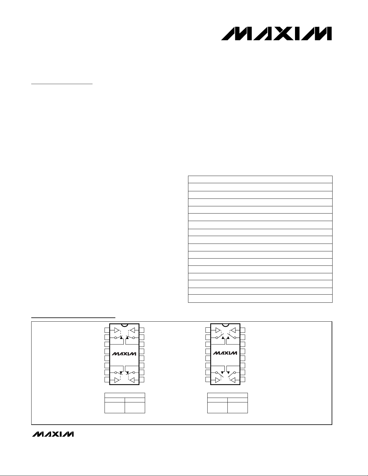
______________Ordering Information
MAX361/MAX362
Precision, Quad, SPST Analog Switches
_______________________________________________________________________ Maxim Integrated Products 1
19-0180; Rev 2; 6/04
16
15
14
13
12
11
10
9
1
2
3
4
5
6
7
8
IN2
COM2
NO2
V+
V-
NO1
COM1
IN1
MAX362
N.C.
NO3
COM3
IN3
IN4
COM4
NO4
GND
DIP/SO
DIP/SO
MAX362
LOGIC SWITCH
0
1
OFF
ON
SWITCHES SHOWN FOR LOGIC "0" INPUT
MAX361
LOGIC SWITCH
0
1
ON
OFF
16
15
14
13
12
11
10
9
1
2
3
4
5
6
7
8
IN2
COM2
NC2
V+
V-
NC1
COM1
IN1
MAX361
N.C.
NC3
COM3
IN3
IN4
COM4
NC4
GND
TOP VIEW
N.C. = Not Internally
Connected
Pin Configurations/Functional Diagrams/Truth Tables
*Contact factory for dice specifications.
PART TEMP RANGE PIN-PACKAGE
MAX361CPE
0°C to +70°C 16 Plastic DIP
MAX361CSE 0°C to +70°C 16 Narrow SO
MAX361C/D 0°C to +70°C Dice*
MAX361EPE -40°C to +85°C 16 Plastic DIP
MAX361ESE -40°C to +85°C 16 Narrow SO
MAX361EJE -40°C to +85°C 16 CERDIP
MAX361MJE -55°C to +125°C 16 CERDIP
MAX362CPE
0°C to +70°C 16 Plastic DIP
MAX362CSE 0°C to +70°C 16 Narrow SO
MAX362C/D 0°C to +70°C Dice*
MAX362EPE -40°C to +85°C 16 Plastic DIP
MAX362ESE -40°C to +85°C 16 Narrow SO
MAX362EJE -40°C to +85°C 16 CERDIP
MAX362MJE -55°C to +125°C 16 CERDIP
For pricing, delivery, and ordering information, please contact Maxim/Dallas Direct! at
1-888-629-4642, or visit Maxim’s website at www.maxim-ic.com.
MAX361ETE -40°C to +85°C 16 Thin QFN
MAX362ETE -40°C to +85°C 16 Thin QFN
Pin Configurations continued at end of data sheet.
Page 2
MAX361/MAX362
Precision, Quad, SPST Analog Switches
2 ________________________________________________________________________________________________
Stresses beyond those listed under “Absolute Maximum Ratings” may cause permanent damage to the device. These are stress ratings only, and
functional operation of the device at these or any other conditions beyond those indicated in the operational sections of the specifications is not implied.
Exposure to absolute maximum rating conditions for extended periods may affect device reliability.
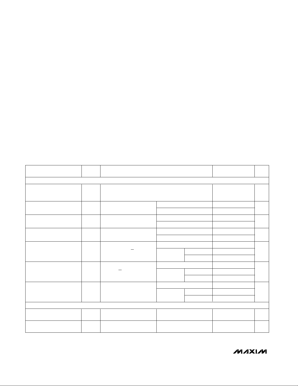
ELECTRICAL CHARACTERISTICS—Dual Supplies
(V+ = 15V, V- = -15V, GND = 0V, V
INH
= 2.4V, V
INL
= 0.8V, TA= T
MIN
to T
MAX
, unless otherwise noted.)
PARAMETER SYMBOL CONDITIONS
MIN TYP MAX
UNITS
(Note 2)
ANALOG
V
COM_
,
Analog-Signal Range V
NO_
, (Note 3) -15 15 V
V
NC_
R
ON
TA= +25°C 50 85
Ω
TA= T
MIN
to T
MAX
100
On Resistance Match
R
ON
TA= +25°C 2
Ω
Between Channels (Note 4)
T
A
= T
MIN
to T
MAX
4
On Resistance Flatness
R
ON
TA= +25°C 9
Ω
(Note 4)
T
A
= T
MIN
to T
MAX
15
Off Leakage Current
I
NO
_
,
T
A
= +25°C -0.50 0.01 0.50
nA
(NO_ or NC_ terminal)
I
NC
_
TA= T
MAX
C, E -4 4
M -20 20
Off Leakage Current
T
A
= +25°C -0.50 0.01 0.50
nA
(COM_ terminal)
I
COM
TA= T
MAX
C, E -4 4
M -20 20
On Leakage Current
I
COM
TA= +25°C -0.50 0.08 0.50
nA
(COM_ and NC_ or NO_
or
T
A
= T
MAX
C, E -6 6
INO, I
NC
M -40 40
DIGITAL
Input Current with
I
INH
V
IN_
= 2.4V -500 0.01 500 nA
Input Voltage High
Input Current with
I
INH
V
IN_
= 0.8V -500 0.01 500 nA
Input Voltage Low
ABSOLUTE MAXIMUM RATINGS
Voltage Referenced to V-
V+ ....................................................................................44V
GND .................................................................................25V
IN_, COM_, NO_, NC_ ...........(V- - 2V) to (V+ + 2V) or 30mA
(whichever occurs first)
Continuous Current (any terminal) .....................................30mA
Peak Current COM, NO, NC
(pulsed at 1ms, 10% duty cycle max)..........................100mA
ESD....................................................................................2000V
Continuous Power Dissipation (T
A
= +70°C) (Note 1)
Plastic DIP (derate 10.53mW/°C above +70°C)..........842mW
Narrow SO (derate 8.70mW/°C above +70°C)............696mW
Thin QFN (derate 33.3mW/°C above +70°C) ............2667mW
CERDIP (derate 10.00mW/°C above +70°C) ..............800mW
Operating Temperature Ranges:
MAX36_C_ _.......................................................0°C to +70°C
MAX36_E_ _ ....................................................-40°C to +85°C
MAX36_MJE..................................................-55°C to +125°C
Storage Temperature Range ............................-65°C to +150°C
Lead Temperature (soldering, 10s) ................................+300°C
Note 1: All leads are soldered or welded to PC board.
I
(NO or NC)
= -10mA,
V
COM_
= 8.5V or -8.5V,
V+ = 13.5V, V- = -13.5V
On Resistance
(COM_ to NO_ or
COM_ to NC_ terminals)
I
(NO or NC)
= -10mA,
V
COM_
= 10V or -10V,
V+ = 15V, V- = -15V
I
(NO or NC)
= -10mA,
V
COM_
= 5V or -5V,
V+ = 15V, V- = -15V
V
COM_
= ±15.5V,
V
NC_
or V
NO_
= +15.5V,
V+ = 16.5V, V- = -16.5V
V
NC_
or V
NO_
= ±15.5V,
V
COM_
= +15.5V,
V+ = 16.5V, V- = -16.5V
V
COM_
= ±15.5V,
V
NC_
or V
NO_
= ±15.5V,
V+ = 16.5V, V- = -16.5V
terminal)
Page 3
MAX361/MAX362
_______________________________________________________________________________________ 3
MAX361/MAX362
Precision, Quad, SPST Analog Switches
_________________________________________________________________________________________________ 3
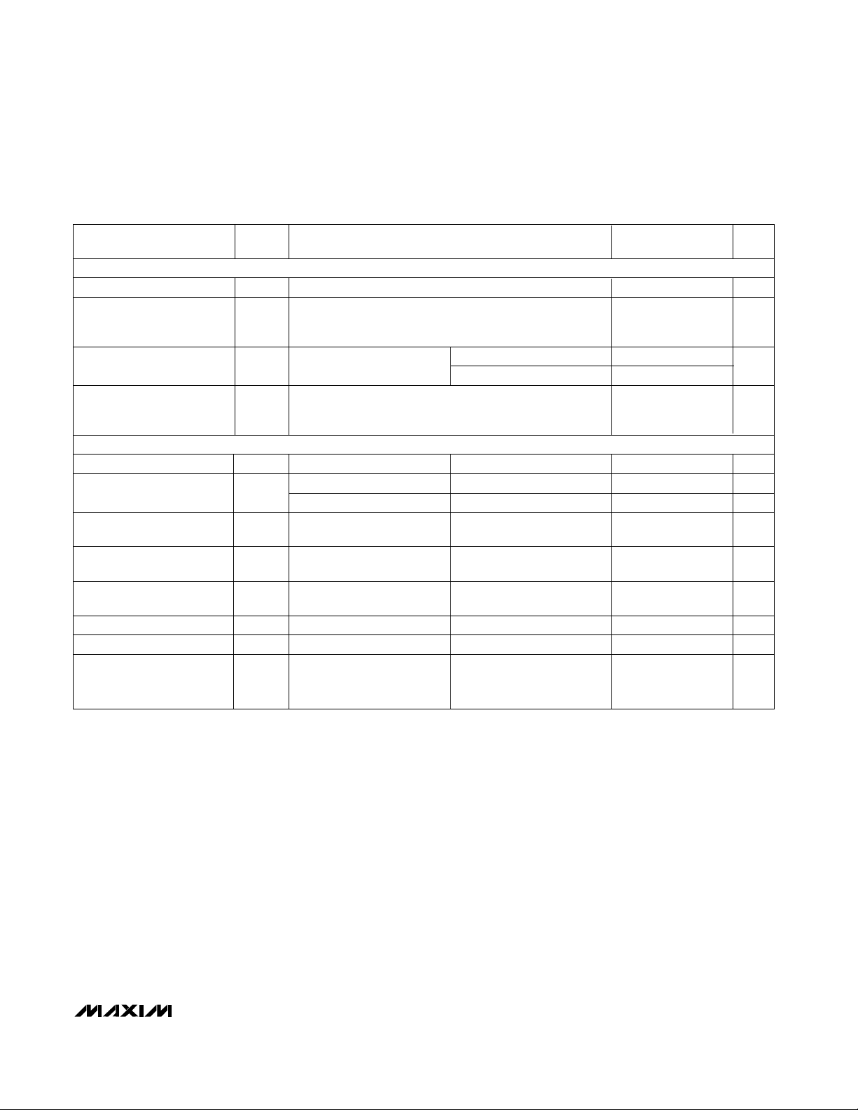
ELECTRICAL CHARACTERISTICS—Dual Supplies (continued)
(V+ = 15V, V- = -15V, GND = 0V, V
INH
= 2.4V, V
INL
= 0.8V, TA= T
MIN
to T
MAX
, unless otherwise noted.)
PARAMETER SYMBOL CONDITIONS
MIN TYP MAX
UNITS
(Note 2)
SUPPLY
Power-Supply Range V+, V- ±4.5 ±20.0 V
All channels on or off, V
IN
= 0V or 5V,
Positive Supply Current I+
V+ = 16.5V, V- = -16.5V
15 100 µA
Negative Supply Current I-
T
A
= +25°C -1 -0.0001 1
µA
TA= T
MIN
to T
MAX
-5 5
All channels on or off, V
IN
= 0V or 5V,
Ground Current I
GND
V+ = 16.5V, V- = -16.5V
-100 -15 µA
DYNAMIC
Turn-On Time t
ON
Figure 1, VS= ±10V, RL= 1kΩ TA= +25°C 150 250 ns
Turn-Off Time t
OFF
MAX361, Figure 1, V
COM
= ±10V TA= +25°C 90 120 ns
MAX362, Figure 1, V
COM
= ±10V TA= +25°C 110 170 ns
Charge Injection Q
C
L
= 1nF, V
GEN
= 0V,
T
A
= +25°C 5 10 pC
R
GEN
= 0Ω, Figure 2
Off Isolation (Note 5) OIRR
R
L
= 50Ω, CL= 5pF,
T
A
= +25°C 60 dB
f = 1MHz, Figure 3
Crosstalk (Note 6)
R
L
= 50Ω, CL= 5pF,
T
A
= +25°C -100 dB
f = 1MHz, Figure 4
Off Capacitance NC or NO C
(OFF)
f = 1MHz, Figure 5 TA= +25°C 4 pF
Off Capacitance COM_ C
COM(OFF)
f = 1MHz, Figure 5 TA= +25°C 4 pF
C
COM(ON)
Channel-On Capacitance f = 1MHz, Figure 5 TA= +25°C 16 pF
All channels on or off,
V
IN
= 0V or 5V,
V+ = 16.5V, V- = -16.5V
Page 4
ELECTRICAL CHARACTERISTICS—Single Supply
(V+ = 12V, V- = 0V, GND = 0V, V
INH
= 2.4V, V
INL
= 0.8V, TA= T
MIN
to T
MAX
, unless otherwise noted.)
PARAMETER SYMBOL CONDITIONS
MIN TYP MAX
UNITS
(Note 2)
SWITCH
V
COM_
,
Analog-Signal Range V
NO_
, (Note 3) 0 12 V
V
NC_
R
ON
TA= +25°C 100 160
Ω
TA= T
MIN
to T
MAX
200
SUPPLY
Power-Supply Range V+ 10 30 V
Positive Supply Current I+ 15 100 µA
Negative Supply Current I-
T
A
= +25°C -1 -0.0001 1 µA
T
A
= T
MIN
to T
MAX
-5 +5
µA
Ground Current I
GND
-100 -15
DYNAMIC
Turn-On Time t
ON
Figure 1, VS= 8V TA= +25°C 300 400 ns
Turn-Off Time t
OFF
Figure 1, VS= 8V TA= +25°C 60 200 ns
Charge Injection Q
CL= 1nF, V
GEN
= 0V,
T
A
= +25°C 5 10 pC
MAX361/MAX362
Precision, Quad, SPST Analog Switches
4 _______________________________________________________________________________________
I
(NC or NO)
= 1.0mA,
V
COM__
= 3V, 8V,
V+ = 10.8V
On Resistance
(COM_ to NO_ or
COM_ to NC_ terminals)
All channels on or off,
V
IN
= 0V or 5V
Note 2: The algebraic convention, where the most negative value is a minimum and the most positive value a maximum, is used in
this data sheet.
Note 3: Guaranteed by design.
Note 4: On resistance match between channels and flatness are guaranteed only with bipolar-supply operation.
Note 5: See Figure 3. Off Isolation = 20 log
10
, V
COM
= output, V
NC or NO
= input to off switch.
Note 6: Between any two switches. See Figure 4.
All channels on or off, VIN= 0V or 5V
All channels on or off, VIN= 0V or 5V
⎛
V
⎜
VNC_ or V
⎝
COM
NO_
⎞
⎟
⎠
Page 5

MAX361/MAX362
Precision, Quad, SPST Analog Switches
_______________________________________________________________________________________ 5
R
(
)
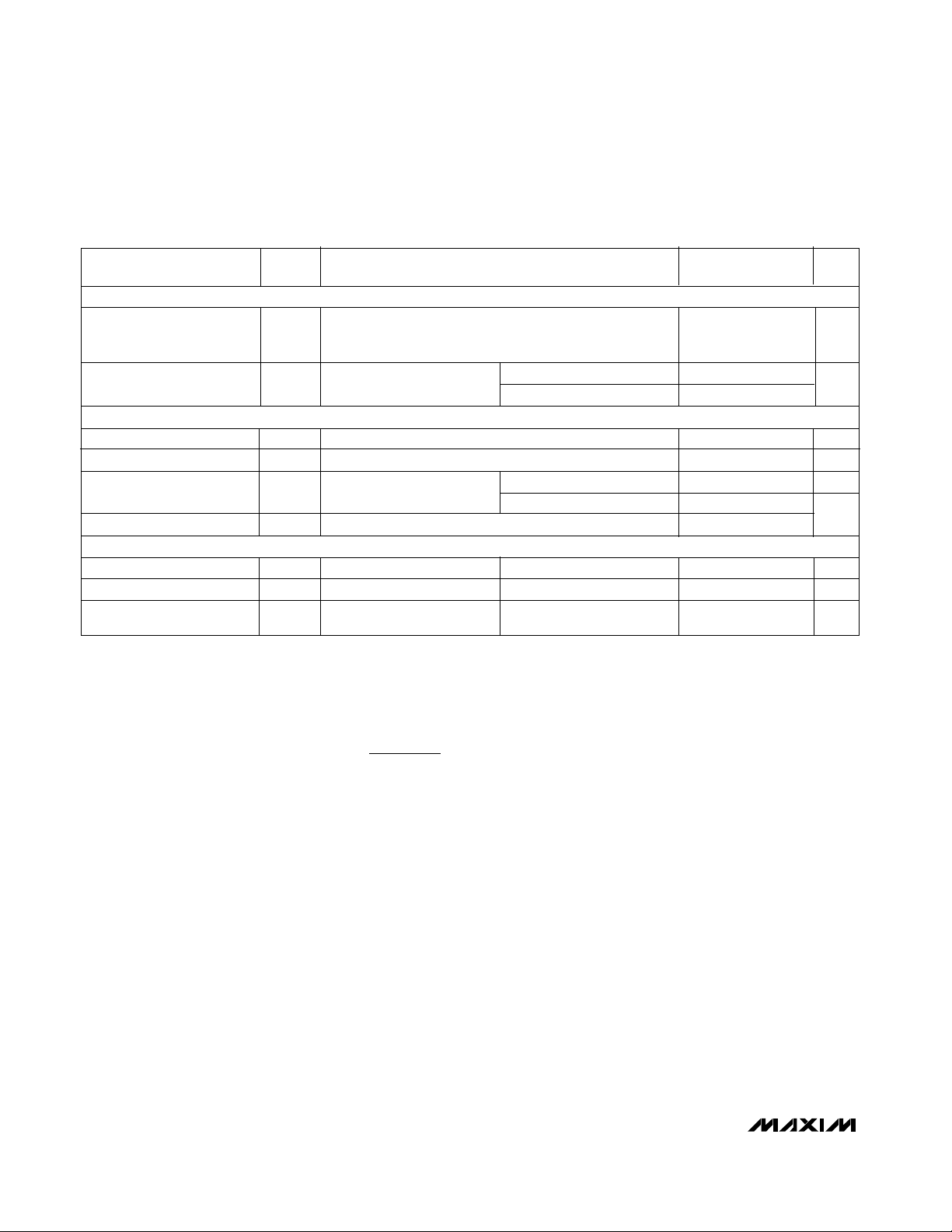
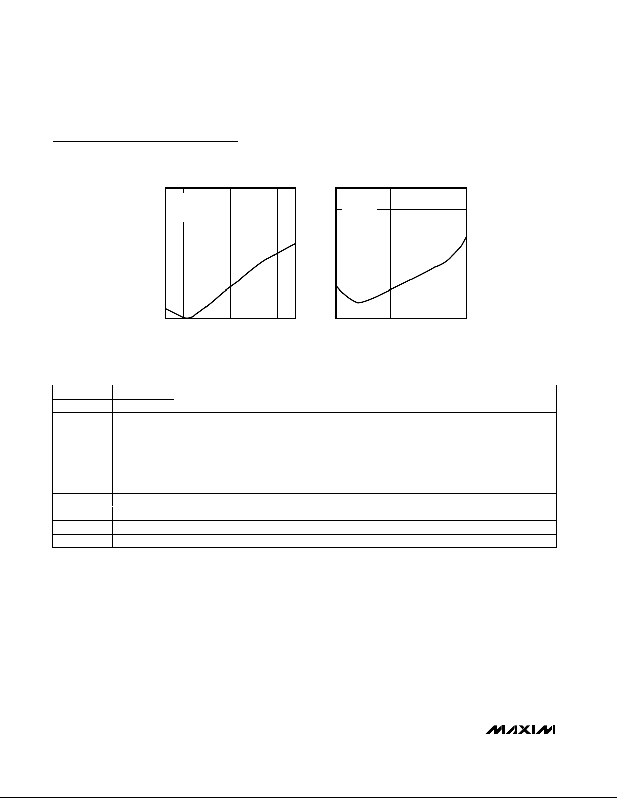
__________________________________________Typical Operating Characteristics
(TA = +25°C, unless otherwise noted.)
ON LEAKAGE CURRENTS
4
3
2
(nA)
COM
TA = +125°C
, I
1
NO_
, I
0
NC_
I
V+ = 15V
-1
V- = -15V
-2
-15 0 15
VNC, VNO ,V
ON RESISTANCE vs. V
COM
TA = +85°C
(V)
AND
COM
UNIPOLAR SUPPLY VOLTAGE
250
225
200
175
150
(Ω)
125
ON
R
100
75
50
25
0
V+ = 10V
V+ = 15V
V+ = 20V
0 5 10 15 20
V
(V)
COM
2
1
(nA)
COM
, I
NO_
TA = +85°C
, I
0
NC_
I
-1
-15 0 15
VNC, VNO, V
ON RESISTANCE vs. V
COM
TA = +125°C
(V)
COM
BIPOLAR SUPPLY VOLTAGE
180
150
OFF LEAKAGE CURRENTS
V
COM
±5V
±10V
±20V
(V)
120
Ω
ON
90
±15V
60
30
0
-20 -10 0 +10 +20
V+ = 15V
V- = -15V
AND
3.5
3.0
2.5
(V)
2.0
IN
V
1.5
0.5
120
100
80
(Ω)
ON
60
R
40
20
SWITCHING THRESHOLD vs.
BIPOLAR SUPPLY VOLTAGE
MAX
MIN
0
±5 ±10 ±15 ±20
BIPOLAR SUPPLY VOLTAGE (V)
ON RESISTANCE vs. V
COM
AND
BIPOLAR VOLTAGE AND TEMPERATURE
V+ = 15V, V- = -15V
TA = +125°C
TA = +25°C
TA = -55°C
0
-14 -7 0 7 14
V
(V)
COM
ON RESISTANCE vs. V
SUPPLY VOLTAGE AND TEMPERATURE
150
125
100
(Ω)
75
ON
R
50
V+ = 12V
25
V- = 0V
0
04 812
TA = +125°C
V
COM
AND UNIPOLAR
COM
TA = +25°C
TA = -55°C
(V)
SWITCHING TIME vs. BIPOLAR
SUPPLY VOLTAGE
240
200
160
120
TIME (ns)
80
40
0
±5 ±10 ±15 ±20
BIPOLAR SUPPLY VOLTAGE (V)
t
ON
SWITCHING TIMES vs. UNIPOLAR
SUPPLY VOLTAGE
350
300
250
200
TIME (ns)
150
t
OFF
100
50
0
10 15 20 24
UNIPOLAR SUPPLY VOLTAGE (V)
t
ON
t
OFF
V- = 0V
Page 6
MAX361/MAX362
Precision, Quad, SPST Analog Switches
6 _______________________________________________________________________________________
Typical Operating Characteristics (continued)
(TA = +25°C, unless otherwise noted.)
CHARGE INJECTION vs.
V
COM
VOLTAGE
Q (pC)
-20
0
20
40
-14 -10 0 10 14
V
COM
(V)
V+ = 15V
V- = -15V
CL = 1nF
CHARGE INJECTION vs.
V
COM
VOLTAGE
Q (pC)
-10
0
10
0 5 10 12
V
COM
(V)
V+ = 12V
V- = 0V
CL = 1nF
___________Applications Information
Operation with Supply Voltages
Other Than ±15V
O
Using supply voltages other than ±15V is reduces the
analog signal range. The MAX361/MAX362 switches
operate with bipolar supplies of ±4.5V to ±20V. Typical
operating characteristic graphs show typical on resistance for ±15V, ±10V, and ±5V supplies. Switching
times increase by a factor of two or more for ±5V operation. The MAX361/MAX362 can also operate from
+10V to +30V unipolar supplies. Both parts can also
be powered from unbalanced supplies such as +24V
and -5V. Connect V- to 0V when operating with a single supply.
Proper power-supply sequencing is recommended for
all CMOS devices. Do not exceed the absolute maximum ratings, because stresses beyond the listed ratings may cause permanent damage to the devices.
Always sequence V+ on first, followed by V-, and logic
inputs. If power-supply sequencing is not possible,
add two small signal diodes in series with the supply
pins for overvoltage protection (Figure 6). Adding the
diodes reduces the analog signal range to 1V below
V+ and 1V below V-, but low switch resistance and low
leakage characteristics are unaffected. Device operation is unchanged, and the difference from V+ to Vshould not exceed +44V.
______________________________________________________________Pin Description
PIN NAME
DIP/SO THIN QFN
1, 16, 9, 8 15, 14, 7, 6 IN1–IN4 Logic Control Input
2, 15, 10, 7 16, 13, 8, 5 COM1–COM4 Analog-Switch Drain Terminal
3, 14, 11, 6 1, 12, 9, 4
4 2 V- Negative-Supply Voltage Input
5 3 GND Ground
12 10 N.C. No Connection. Not internally connected
13 11 V+ Positive-Supply Voltage Input—Connected to Substrate
— EP PAD Exposed Pad—Connect pad to V+
NAME FUNCTION
NO1–NO4 or
NC1–NC4
NC (normally closed, MAX361)
NO (normally open, MAX362)
Analog-Switch Terminal
Page 7
MAX361/MAX362
Precision, Quad, SPST Analog Switches
_______________________________________________________________________________________ 7
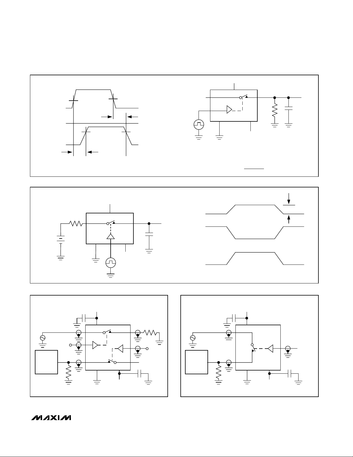
Figure 1. Switching-Time Test Circuit
Figure 2. Charge-Injection Test Circuit
Figure 3. Crosstalk Test Circuit (repeat for channels 3 and 4)
Figure 4. Off-Isolation Test Circuit
LOGIC
+3V
INPUT
SWITCH
INPUT
SWITCH
OUTPUT
0V
V
COM
0V
50%
V
O
0.8V
O
t
ON
LOGIC INPUT WAVEFORM IS INVERTED FOR SWITCHES
THAT HAVE THE OPPOSITE LOGIC SENSE.
R
GEN
COM_
V
GEN
IN_GND
+15V
V+
t
OFF
t
f
t
r
NO_
OR NC_
V-
< 20ns
< 20ns
0.8V
+15V
SWITCH
INPUT
1N_
LOGIC
INPUT
O
V
O
C
L
+3V
MAX361
COM_
V
COM
GND
REPEAT TEST FOR CHANNELS 2, 3, AND 4.
FOR LOAD CONDITIONS, SEE SPECIFICATIONS
CL (INCLUDES FIXTURE AND STRAY CAPACITANCE)
V
O
IN_
VO = V
NO_ OR NC_
V+
COM
V-
-15V
R
L
+ R
V
O
R
L
RL
ON
35pF
∆V
O
OFFONOFF
-15V
VIN = +3V
+15V
C
SIGNAL
GENERATOR
ANALYZER
R
GEN
0.8V, 2.4V
10dBm
= 50Ω
R
L
V+
COM1
IN1
NC2 OR NO2
GND
NC1 OR NO1
IN2
COM2
V-
-15V
50Ω
0.8V, 2.4V
C
OFF OFFON
MAX362
SIGNAL
GENERATOR
ANALYZER
IN_
R
GEN
10dBm
= 50Ω
R
L
C
Q = ∆VO × C
+15V
V+
COM
NC_ OR
NO_
GND
L
IN_
V-
-15V
0.8V, 2.4V
C
Page 8
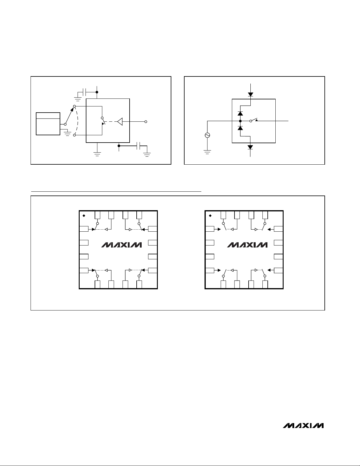
Figure 5. Channel Capacitance Test Circuit Figure 6. Overvoltage Protection Using Blocking Diodes
TRANSISTOR COUNT: 126;
SUBSTRATE CONNECTED TO V+.
Pin Configurations (continued)
MAX361/MAX362
Precision Quad SPST Analog Switches
8 _______________________________________________________________________________________
V+
V-
METER
IMPEDANCE
ANALYZER OR
EQUIVALENT
f = 1MHz
C
COM_
NO_
OR
NC_
+15V
+V
GND
V+
COM_
V
g
V-
-15V
IN_
0.8V, 2.4V
C
TOP VIEW
COM1
16
1NC11
2V-
3GND
IN1
15
IN2
MAX361
COM2
14
13
12 NC2
11 V+
10 N.C.
IN1
IN2
MAX362
COM2
12
11
10
NO1
GND
COM1
16 15 14 13
1
2
V-
3
NC_ OR NO_
NO2
V+
N.C.
8
COM3
9
NC3
NO4
4
6
5
COM4
(5mm x 5mm)
7 8
IN4
IN3
THIN QFN
COM3
NC4
4
5
6
7
IN4
COM4
(5mm x 5mm)
IN3
THIN QFN
9
NO3
Page 9
MAX361/MAX362
Precision Quad SPST Analog Switches
_______________________________________________________________________________________ 9
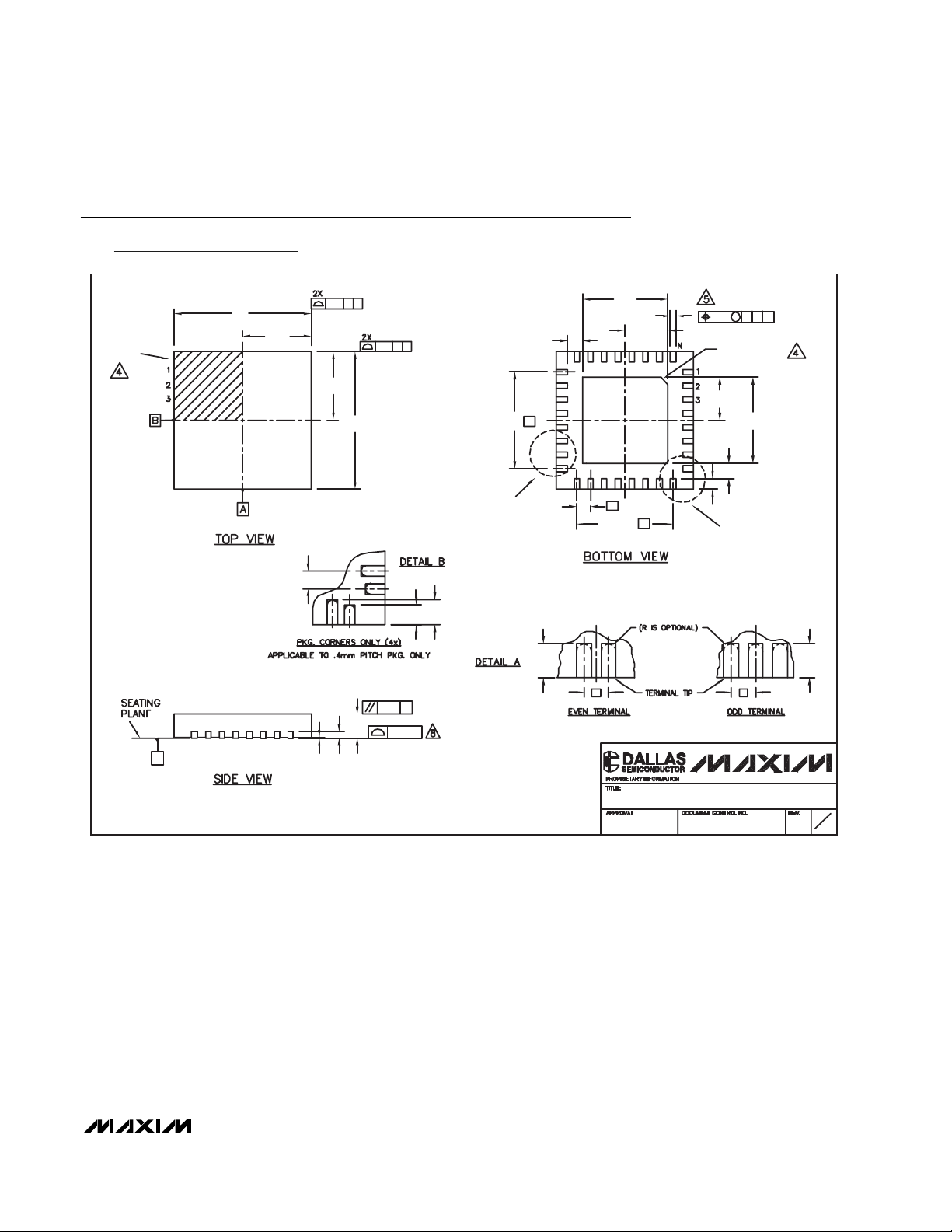
Package Information
(The package drawing(s) in this data sheet may not reflect the most current specifications. For the latest package outline information,
go to www.maxim-ic.com/packages
.)
D/2
e
(ND-1) X e
L
D2
b
C
L
D2/2
0.10 M C A B
PIN # 1 I.D.
0.35x45∞
E2/2
L
DETAIL B
C
E2
L
k
CC
L
LL
0.15 C A
0.15
C B
E/2
E
e
L
L1
(NE-1) X e
DETAIL A
k
D
PIN # 1
I.D.
QFN THIN.EPS
0.10 C
A
0.08 C
C
A1 A3
e e
PACKAGE OUTLINE
16, 20, 28, 32, 40L, THIN QFN, 5x5x0.8mm
21-0140
1
E
2
Page 10
MAX361/MAX362
Precision Quad SPST Analog Switches
Maxim cannot assume responsibility for use of any circuitry other than circuitry entirely embodied in a Maxim product. No circuit patent licenses are
implied. Maxim reserves the right to change the circuitry and specifications without notice at any time.
10 ____________________Maxim Integrated Products, 120 San Gabriel Drive, Sunnyvale, CA 94086 408-737-7600
© 2004 Maxim Integrated Products Printed USA is a registered trademark of Maxim Integrated Products.
Package Information (continued)
(The package drawing(s) in this data sheet may not reflect the most current specifications. For the latest package outline information,
go to www.maxim-ic.com/packages
.)
COMMON DIMENSIONS
PKG.
SYMBOL
A
A1
A3
b
D
E
e
k
L
L1
N
ND
NE
JEDEC
NOTES:
1. DIMENSIONING & TOLERANCING CONFORM TO ASME Y14.5M-1994.
2. ALL DIMENSIONS ARE IN MILLIMETERS. ANGLES ARE IN DEGREES.
3. N IS THE TOTAL NUMBER OF TERMINALS.
4. THE TERMINAL #1 IDENTIFIER AND TERMINAL NUMBERING CONVENTION SHALL CONFORM TO JESD 95-1
SPP-012. DETAILS OF TERMINAL #1 IDENTIFIER ARE OPTIONAL, BUT MUST BE LOCATED WITHIN THE
ZONE INDICATED. THE TERMINAL #1 IDENTIFIER MAY BE EITHER A MOLD OR MARKED FEATURE.
5. DIMENSION b APPLIES TO METALLIZED TERMINAL AND IS MEASURED BETWEEN 0.25 mm AND 0.30 mm
FROM TERMINAL TIP.
6. ND AND NE REFER TO THE NUMBER OF TERMINALS ON EACH D AND E SIDE RESPECTIVELY.
7. DEPOPULATION IS POSSIBLE IN A SYMMETRICAL FASHION.
8. COPLANARITY APPLIES TO THE EXPOSED HEAT SINK SLUG AS WELL AS THE TERMINALS.
9. DRAWING CONFORMS TO JEDEC MO220, EXCEPT EXPOSED PAD DIMENSION FOR T2855-1,
T2855-3 AND T2855-6.
10. WARPAGE SHALL NOT EXCEED 0.10 mm.
16L 5x5
MIN. MAX.NOM.
0.70 0.800.75
0.02
0.20 REF.
0.25
4.90
5.00
4.90
0.80 BSC.
0.250--
0.30 0.500.40
---
16
4
4
WHHB
0.05
0.350.30
5.10
5.105.00
MIN.
0.70
0
0.20 REF.
0.25
4.90
4.90
0.65 BSC.
0.25
0.45
---
20L 5x5
NOM.
0.75
0.02
0.30
5.00
5.00
0.55
20
5
5
WHHC
MAX.
0.80
0.05
0.35
5.10
5.10
0.65
MIN.
0.70
0
0.20
4.90
4.90
--
0.25
0.45
---
28L 5x5
NOM.
0.75
0.02
0.20 REF.
0.25
5.00
5.00
0.50 BSC.
0.55
28
7
7
WHHD-1
MAX.
MIN.
0.80
0.70
0.05
0
0.30
0.20 0.25 0.30
5.10
4.90
5.10
4.90
--
0.25
0.65
0.30
32L 5x5
NOM.
0.75
0.02
0.20 REF.
5.00
5.00
0.50 BSC.
0.40
---
32
8
8
WHHD-2
MAX.
MIN.
0.80
0.70
0.05
0
0.15
5.10
4.90
5.10
4.90
--
0.25
0.50
0.40
0.30 0.40 0.50
40L 5x5
NOM.
0.75
-
0.20 REF.
0.20
5.00
5.00
0.40 BSC.
0.35 0.45
0.50
40
10
10
-
EXPOSED PAD VARIATIONS
PKG.
CODES
MAX.
T1655-1
0.80
0.05
0.25
5.10
T2855-1 3.25 3.353.15 3.25
5.10
T2855-2 2.60 2.602.80 2.70 2.80
T2855-3 3.15 3.25 3.35 3.15 3.25 3.35
T2855-4 2.60 2.70 2.80 2.60 2.70 2.80
0.60
T2855-5 2.60 2.70 2.80 2.60 2.70 2.80
T2855-6 3.15 3.25 3.35 3.15 3.25 3.35
T2855-7 2.60 2.70
T3255-2
D2
MAX.
NOM.MIN.
3.203.00 3.10 3.00 3.10 3.20
3.203.00T1655-2 3.10 3.00 3.10 3.20 YES
3.00T2055-2 3.10
3.00
3.00 3.10T3255-3 3.203.00 3.10
3.20
3.353.15
2.70
2.80
3.20
3.10
3.20
3.203.00 3.10T3255-4 3.203.00 3.10
3.403.20 3.30T4055-1 3.20 3.30 3.40
PACKAGE OUTLINE
16, 20, 28, 32, 40L, THIN QFN, 5x5x0.8mm
MIN.E2NOM. MAX.
3.203.00 3.10
3.103.00 3.203.103.00 3.20T2055-4
2.60 2.70 2.80
3.00 3.10 3.20
21-0140
DOWN
BONDS
ALLOWED
NO
NO
YES3.103.00 3.203.103.00 3.20T2055-3
NO
NO
NO
YES
YES
NO
NO
YES
NO
YES
NO
YES
E
2
2
 Loading...