Maxim MAX3580 Datasheet
General Description
The MAX3580 fully integrated, direct-conversion TV tuner
is designed for Digital Video Broadcasting-Terrestrial
(DVB-T) applications. The integrated tuner covers a
170MHz to 230MHz input frequency range for the VHF-III
band and 470MHz to 878MHz for the UHF band.
The MAX3580 direct-conversion tuner integrates an RF
input switch and a multiband tracking filter, allowing
low-power tuner-on-board applications without the cost
and power-dissipation issues of dual-conversion tuner
solutions. The zero-IF architecture eliminates the need
for SAW filters by providing baseband I and Q outputs
directly to the demodulator. In addition, DC-offset cancellation is implemented on-chip using a mixed-signal
architecture to improve the second-order distortion performance and the dynamic range of the downstream
digitizer and demodulator.
The MAX3580 features dynamic gain control of more
than 76dB and a typical midband noise figure of 4.7dB
referred to the LNA input. The VCO architecture optimizes both in-band and wideband phase noise for
OFDM applications where sensitivity to both 1kHz
phase noise and wideband phase noise related to
strong adjacents can be a problem.
The MAX3580 communicates using a 2-wire serial bus.
The device operates from a typical +3.3V power supply
and dissipates 650mW. The MAX3580 is available in a
small 32-pin thin QFN package (5mm x 5mm) with an
exposed paddle. Electrical performance is guaranteed
over the extended -40°C to +85°C temperature range.
Applications
Digital Televisions
Digital Terrestrial Set-Tops
Laptop Televisions
Automotive Televisions
USB Peripherals
Features
o 650mW Power Dissipation (at VCC= +3.3V)
o I and Q Baseband Outputs Eliminate All IF-SAW
Filters
o Integrated RF Tracking Filters
o Tunable Baseband Lowpass Filters
o Full-Band VHF-III and UHF Tuning
o +38dB Digital ACPR, +47dB Analog ACPR
o Low Noise Figure: 4.7dB (typ)
o Frac-N Synthesizer for -90dBc/Hz Close-In
Phase Noise
o Baseband Overload Detector Controls RF AGC if
Desired
o +3.1V to +3.5V Supply Voltage Range
o Ultra-Small, 5mm x 5mm Thin QFN Package
MAX3580
Direct-Conversion TV Tuner
________________________________________________________________
Maxim Integrated Products
1
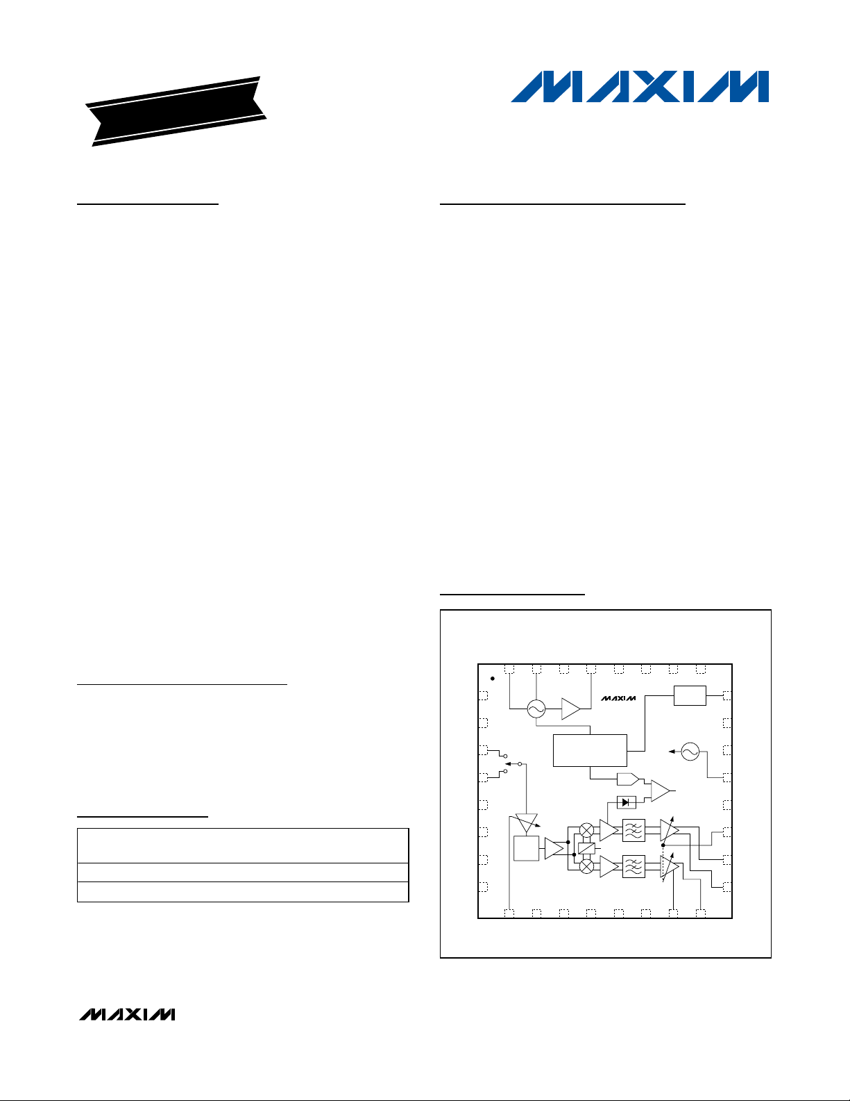
Pin Configuration/
Functional Diagram
Ordering Information
TRACKING
FILTER
GND_TUNE
LDO
XE
XB
VCC_VCO
MUX
RFIN2
ADDR2
LEXT
VCC_SYN
RFIN
RF_AGC
SCL
SDA
BBI-
BBQ-
BBQ+
BB_AGC
BBI+
VCC_BB
REF_BUFF
VCC_RF
OVLD_DET
IND1
IND2
VCC_XTAL
VTUNE
CP
OVLD_DET
GND_LNA
GND_CP
GND_PLL
N.C.
TOP VIEW
32 28
293031
25
26
27
10
13
15
14
1611 12
9
17
18
19
20
21
22
23
24
2
3
4
5
6
7
8
1
MAX3580
0
90
DAC
LO
LO
CHARGE
PUMP
SERIAL INT ERFACE, CON TROL,
AND
SYNTHESIZER
19-0611; Rev 1; 5/07
For pricing, delivery, and ordering information, please contact Maxim/Dallas Direct! at
1-888-629-4642, or visit Maxim’s website at www.maxim-ic.com.
*
EP = Exposed paddle.
+
Denotes lead-free package.
T
= Tape-and-reel package.
EVALUATION KIT
AVAILABLE
PART TEMP RANGE
MAX3580ETJ+ -40°C to +85°C 32 TQFN-EP* T3255-5
MAX3580ETJ+T -40°C to +85°C 32 TQFN-EP* T3255-5
PIN-
PACKAGE
PKG
CODE
MAX3580
Direct-Conversion TV Tuner
2 _______________________________________________________________________________________
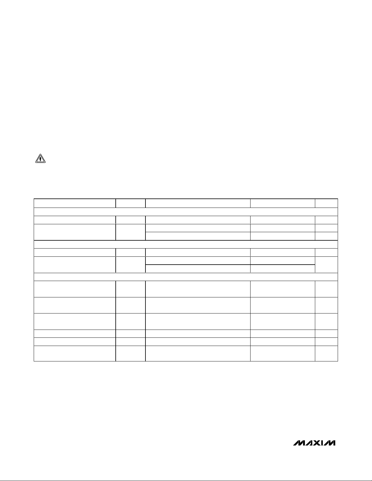
ABSOLUTE MAXIMUM RATINGS
DC ELECTRICAL CHARACTERISTICS
(MAX3580 EV kit, VCC= +3.1V to +3.5V, GND = 0V, BB_AGC = RF_AGC = +2.85V, RF input terminated into a 75Ω load, BBI_ and
BBQ_ are open, no input signal, VCO active, registers set according to the specified default register conditions, T
A
= -40°C to
+85°C, unless otherwise specified. Typical values are at V
CC
= +3.3V, TA=+25°C, unless otherwise specified.) (Note 1)
Stresses beyond those listed under “Absolute Maximum Ratings” may cause permanent damage to the device. These are stress ratings only, and functional
operation of the device at these or any other conditions beyond those indicated in the operational sections of the specifications is not implied. Exposure to
absolute maximum rating conditions for extended periods may affect device reliability.
VCCto GND...........................................................-0.3V to +3.6V
SDA, SCL, ADDR2, MUX, REF_BUFF,
BB_AGC, RF_AGC to GND ................................-0.3V to +3.6V
All Other Pins to GND ..............................-0.3V to (+V
CC
+ 0.3V)
RF Input Power ...............................................................+10dBm
Operating Temperature Range ...........................-40°C to +85°C
Junction Temperature......................................................+150°C
Storage Temperature Range .............................-65°C to +165°C
Continuous Power Dissipation (T
A
= +70°C)
(derate 21.3mW/°C above +70°C)..............................1702mW
Lead Temperature (soldering, 10s) .................................+300°C
CAUTION! ESD SENSITIVE DEVICE
SUPPLY VOLTAGE AND CURRENT
Supply Voltage V
Supply Current I
PARAMETER SYMBOL CONDITIONS MIN TYP MAX UNITS
CC
CC
Active 197 225 mA
Shutdown mode 200 µA
RF_AGC AND BB_AGC
Input Bias Current I
RF and Baseband AGC Control
Voltage
V
AGC
AGC
V
at +0.5V and +2.85V -50 +50 µA
AGC
Maximum gain 2.85
Minimum gain 0.5
SERIAL INTERFACE AND MUX OUTPUT (SCL, SDA, MUX)
Input Logic-Level Low V
Input Logic-Level High V
IL
IH
Input Hysteresis
SDA, SCL Input Current -10 +10 µA
Output Logic-Level Low V
Output Logic-Level High V
OL
OH
Sink current = 0.3mA 0.4 V
Source current = 0.3mA
3.1 3.5 V
0.7 x
V
CC
V
-
CC
0.5
V
0.05 x
V
CC
V
0.3 x
V
CC
V
V
V
MAX3580
Direct-Conversion TV Tuner
_______________________________________________________________________________________ 3
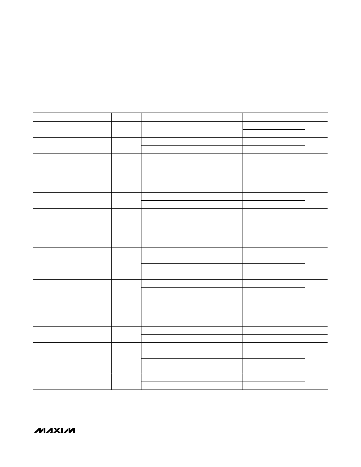
AC ELECTRICAL CHARACTERISTICS
(MAX3580 EV kit, VCC= +3.1V to +3.5V, GND = 0V. RF_AGC = BB_AGC = +2.85V, RF input terminated into a 75Ω load, BBI_ and
BBQ_ loaded by R
L
greater than 2kΩ and CLless than 10pF, VCO active, registers are set according to the recommended default
register conditions, T
A
= -40°C to +85°C, unless otherwise noted. Typical values are at VCC= +3.3V, TA= +25°C, unless otherwise
noted.) (Note 1)
Operating Frequency Range f
Overall Voltage Gain (Note 2)
RF Gain Flatness W i thi n each V H F- III and U H F b and ( N ote 10) -3 +3 dB
PARAMETER SYMBOL CONDITIONS MIN TYP MAX UNITS
RF
Gain specification met across this
frequency band
RF_AGC = BB_AGC = +2.85V 74
RF_AGC = BB_AGC = +0.5V 26
170 230
470 878
MHz
dB
Input Return Loss Wor st case acr oss b and sel ected , 75Ω system 7 dB
230MHz 5.4
Noise Figure (DSB) (Notes 3, 4) NF
470MHz 4.7
dB
858MHz 6.5
Input 2nd-Order Intercept Point IIP2
Broadband (Notes 4, 5) 12
Br oad b and , RF_AGC ad j usted for 49d B of g ai n > 26
dBm
Broadband (Notes 4, 6) > -4
Br oad b and , RF_AGC ad j usted for 49d B of g ai n > 12
RF 1dB Desense
LO Harmonic Reception
RF Channel Flatness
Isolation
Quadrature Accuracy
Narrowband (Notes 4, 7) -15 Input 3rd-Order Intercept Point IIP3
Narrowband, RF_AGC adjusted for 49dB of
gain (Note 7)
P
DESIRED
3.75MHz, P
RF_AGC adjusted for 49dB of gain,
P
DESIRED
= -78dBm and converted to
10MHz higher (Note 4)
TONE
= -55dBm
3
-24
-1
RF i np ut r ang e of 170M H z to 960M H z ( N ote 8) -60
RF input range of 960MHz to 1400MHz > -40
8MHz RF channel at baseband, tested at
169MHz and 469MHz
DC to 30MHz, RF input to baseband output,
relative to desired channel
-1 +1 dB
> 60 dBc
I/Q phase error at 1MHz -3 +3 D eg r ees
I/Q amplitude error at 1MHz -1.5 +1.5 dB
dBm
dBm
dBc
50MHz to 470MHz -50 -20
Spurious at the RF Input (Note 3)
470MHz to 878MHz -50 -35
878MHz to 1732MHz < -50 -20
dBmV
At 1kHz to 10kHz (Note 3) -80 -90
Phase Noise (Single-Sideband,
Closed Loop)
ΦN
At 100kHz (Note 3) -94 -107
dBc/Hz
At 1MHz -130
MAX3580
Direct-Conversion TV Tuner
4 _______________________________________________________________________________________
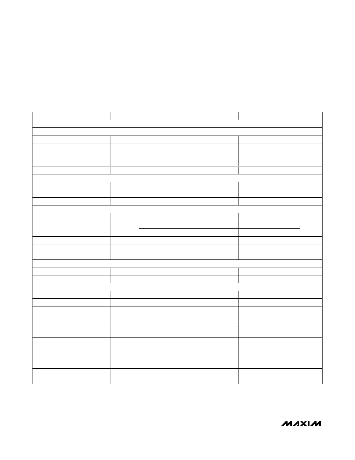
AC ELECTRICAL CHARACTERISTICS (continued)
(MAX3580 EV kit, VCC= +3.1V to +3.5V, GND = 0V. RF_AGC = BB_AGC = +2.85V, RF input terminated into a 75Ω load, BBI_ and
BBQ_ loaded by R
L
greater than 2kΩ and CLless than 10pF, VCO active, registers are set according to the recommended default
register conditions, T
A
= -40°C to +85°C, unless otherwise noted. Typical values are at VCC= +3.3V, TA= +25°C, unless otherwise
noted.) (Note 1)
SIGMA-DELTA FRACTIONAL-N SYNTHESIZER
REFERENCE OSCILLATOR
Frequency f
Input Impedance Z
Voltage Gain 30 V/V
Output Impedance Z
Buffered Output 10kΩ || 10pF load 0.7 V
DIVIDERS
RF N Divider Ratio (Notes 12, 13) 12 251 —
RF R Divider Ratio VHF band operation requires R divider = 2 1 2 —
Fractional-N Resolution 20 Bits
LO PHASE DETECTOR AND CHARGE PUMP
Phase-Detector Frequency 4 27 MHz
Charge-Pump Current I
Charge-Pump Tri-State Current -10 +10 µA
Charge-Pump Compliance
Range
LOCAL OSCILLATOR
Tuning Frequency Range f
VCO Dividers 4 16 —
BASEBAND STAGE
Nominal Output Voltage (Note 2) 1 V
1dB Output Compression Point P
Output Impedance Differential 60 Ω
Passband AGC Range BB_AGC = 0.5V to 2.85V 30 50 dB
Passband Cutoff Attenuation
Passband Differential Gain Error
Passband Group Delay
Group Delay Mismatch
PARAMETER SYMBOL CONDITIONS MIN TYP MAX UNITS
REF
IN
OUT
CP
OSC
1dB
Gain = 0 600
Gain = 1 1200
Charge-pump positive to negative current
matching of ≤ ±5%
Tank Frequency 2160 4400 MHz
Differential voltage at 3MHz 1.6 2 V
At 3.8MHz (UHF Mode);
at 3.325MHz (VHF Mode)
2MHz to 3.8MHz, I channel vs. Q channel
(UHF mode)
From DC to 3.8MHz over any 1.1kHz band
(UHF mode)
From 0.1MHz to 3.8MHz, I channel vs. Q
channel (UHF mode) (Note 9)
4 27 MHz
10 kΩ
15 Ω
VCC -
0.4
0.4
2 5 dB
-0.45 +0.45 dB
5 ns
< 2 ns
µA
P-P
V
P-P
P-P
MAX3580
Direct-Conversion TV Tuner
_______________________________________________________________________________________ 5
AC ELECTRICAL CHARACTERISTICS (continued)
(MAX3580 EV kit, VCC= +3.1V to +3.5V, GND = 0V. RF_AGC = BB_AGC = +2.85V, RF input terminated into a 75Ω load, BBI_ and
BBQ_ loaded by R
L
greater than 2kΩ and CLless than 10pF, VCO active, registers are set according to the recommended default
register conditions, T
A
= -40°C to +85°C, unless otherwise noted. Typical values are at VCC= +3.3V, TA= +25°C, unless otherwise
noted.) (Note 1)
Note 1: Min and Max limits are guaranteed by test above TA= +25°C and are guaranteed by design and characterization at
T
A
= -40°C. The default register settings are not production tested. Load registers no sooner than 100µs after power-up.
Note 2: The specified overall voltage gain is suitable to amplify -93dBm to -20dBm to 1V
P-P
at the baseband output.
Note 3: Guaranteed by design characterization over the specified operating conditions. Not production tested.
Note 4: BB_AGC adjusted for gain = 72dB with RF_AGC at 2.85V.
Note 5: Two tones at a) 230MHz and 431MHz with IM measured at 201MHz and b) 230MHz and 701MHz with IM measured at
471MHz.
Note 6: Two tones at 499MHz and 689MHz with IM measured at 879MHz.
Note 7: IM3 measured with two tones within the adjacent channel. Production tested at 72dB of gain with two tones at a)
205.75MHz and 210.5MHz with IM measured at 201MHz and b) 475.25MHz and 479.5MHz with IM measured at
471MHz. Production tested at 49dB of gain with two tones at 475.25MHz and 479.5MHz with IM measured at 471MHz.
Note 8: Measured at RF = 171MHz with harmonics at 511MHz (3rd harmonic) and 851MHz (5th harmonic).
Note 9: Delay of 2ns equal 2.74° phase error.
Note 10: UHF rolloff of 4dB in addition to gain flatness specification.
Note 11: Production tested at V
CC
= +3.5V to limits of 1.7V -0.12/+0.1V.
Note 12: Operation in the VHF band requires the R divider = 2.
Note 13: Operation of the N divider at values below 12 is not tested or guaranteed.
Rejection Ratio
DC Output Voltage V
Output DC Offset BB_AGC = 2.85V -70 +70 mV
Baseband Highpass Cutoff Programmable 20 to 200 Hz
AGC Gain Slope BB_AGC = 0.5V to 2.85V 14 35 dB/V
Ratio of Passband to Stopband
Noise
PARAMETER SYMBOL CONDITIONS MIN TYP MAX UNITS
At 5.25MHz (UHF mode) 23
At 4.75MHz (VHF mode) 23
V
dB
DC
At 13.25MHz (UHF mode) 63
At 11.75MHz (VHF mode) 62
At > 16.2MHz
CM
Common mode (Note 11) 0.485 x V
BB_AGC = 2.85V, 10kHz to 3.8MHz vs.
16.2MHz to 23.8MHz
84
CC
15 dB
MIXER OVERLOAD DETECTOR (RSSI)
Attack-Point Accuracy 5.25MHz test tone ±1 dB
Attack-Point Increment 3-bit DAC 1.5 dB
Detector Output Sink
Detector on, V
Detector off, V
= 0.5V 0.3 mA
OUT
= 2.85V 5 µA
OUT
Detector Gain 30 V/V
Detector Response Time < 200 µs
2-WIRE INTERFACE
Clock Rate 400 kHz
MAX3580
Direct-Conversion TV Tuner
6 _______________________________________________________________________________________
Performance to Standards
The following is selected overall performance data for the
MAX3580 + digital demodulator.
Table 1 shows the typical overall performance as measured using the MAX3580 and one current production
DVB-T demodulator. This reference design is available
in NIM card form factor upon request.
MBRAI refers to standard MBRAI 04-102 IEC 62002-1
available from www.ansi.org.
NorDig refers to standard Unified 1.0.2 available from
www.nordig.org.
Modulation of wanted and interfering channel(s) is 8k
mode, 16 QAM, C/R = 3/4, GI = 1/4, sensitivity or
immunity Reference Bit Error Rate is 2 x 10e-4, unless
stated otherwise.
Table 1. Selected Typical MBRAI and NorDig Performance
TEST SCENARIO COMMENTS SPEC MINIMUM MAX3580 TYPICAL
MBRAI S2 Immunity/ACPR for N ±1 adjacent ch. 29dB 40dB
MBRAI S2 Immunity/ACPR N ±2 alternate ch. 40dB 43dB
MBRAI L3 Li near ity/c r ossm od . w i th N +2 and N +4 ch. 40dB 47dB
NorDig 16 QAM 2/3 S ensi ti vi ty at channel 21 ( 470 M H z) -84.1dBm -85.1dBm
NorDig QPSK 1/2 Sensitivity at channel 42 (642 MHz) -92.1dBm -94.8dBm
NorDig 64 QAM 7/8 Sensitivity at channel 59 (778 MHz) -74.7dBm -76dBm
MAX3580
Direct-Conversion TV Tuner
_______________________________________________________________________________________
7
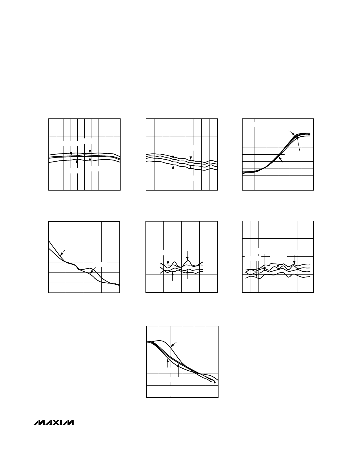
Typical Operating Characteristics
(Typical values are at VCC= +3.3V, TA= +25°C, unless otherwise noted.)
0
10
5
20
15
25
30
VHF MODE NOISE FIGURE
vs. VOLTAGE GAIN
MAX3580 toc07
VOLTAGE GAIN (dB)
NOISE FIGURE (dB)
60 70 7565 80 85 90
TA = +25°C, +55°C
TA = -40°C
TA = +85°C
fRF = 220MHz
BB_AGC = 2.85V
VHF-III BAND VOLTAGE GAIN
vs. FREQUENCY
110
100
TA = +25°C
90
GAIN (dB)
80
70
150 170 180 190 200160 210 220 230 240 250
TA = +85°C
TA = 0°C
TA = +55°C
FREQUENCY (MHz)
PHASE NOISE vs. OFFSET FREQUENCY
-50
-60
-70
-80
-90
PHASE NOISE (dBm/Hz)
-100
-110
-120
620MHz
220MHz
0.1 1 10 100 1000
OFFSET FREQUENCY (kHz)
MAX3580 toc01
MAX3580 toc04
110
100
90
GAIN (dB)
80
70
20
15
10
NOISE FIGURE (dB)
UHF BAND VOLTAGE GAIN
vs. FREQUENCY
TA = +25°C
TA = +85°C
450 550 600 650 700500 750 800 850 900
FREQUENCY (MHz)
NOISE FIGURE vs. VHF FREQUENCY
TA = +55°C
5
TA = -40°C
0
150 175 200 225 250
FREQUENCY (MHz)
TA = 0°C
TA = +55°C
TA = +85°C
TA = +25°C
MAX3580 toc02
MAX3580 toc05
VOLTAGE GAIN
vs. RF_AGC CONTROL VOLTAGE
110
BB_AGC = 2.85V
100
90
80
70
60
GAIN (dB)
50
40
30
20
10
01.00.5 1.5 2.0 2.5 3.0
RF_AGC CONTROL VOLTAGE (V)
TA = -40°C
TA = +25°C, +55°C
TA = +85°C
NOISE FIGURE vs. UHF FREQUENCY
20
15
TA = +25°C
10
TA = -40°C
NOISE FIGURE (dB)
5
0
450 550 600 650 700500 750 800 850 900
TA = +55°C
FREQUENCY (MHz)
TA = +85°C
MAX3580 toc03
MAX3580 toc06
 Loading...