

19-0389; Rev. 2; 9/96
Fault-Protected Analog Multiplexers
_______________General Description
The MAX354/MAX355 fault-protected multiplexers
(muxes) use a series N-channel, P-channel, N-channel
structure that protects the devices from overvoltage up
to 40V beyond the supply rails during power-up, powerdown, and fault conditions. The MAX354/MAX355 also
protect sensitive circuit components against voltages
near or beyond the normal supplies.
The MAX354 single 8-channel mux and the MAX355
dual 4-channel mux protect analog signals while operating from a single 4.5V to 36V supply or ±4.5V to ±18V
dual supplies. These muxes have 350Ω on-resistance
and can be used for demultiplexing as well as multiplexing. Input leakage current is less than 0.5nA at
+25°C and less than 5nA at +85°C.
All digital inputs have 0.8V and 2.4V logic thresholds,
ensuring both TTL and CMOS logic compatibility without pull-up resistors. Break-before-make operation is
guaranteed and power consumption is less than
1.5mW.
________________________Applications
Data-Acquisition Systems
Industrial and Process Control
Avionics
ATE Equipment
Signal Routing
Redundant/Backup Systems
____________________________Features
♦ 350Ω Max On-Resistance
♦ Improved 2nd Source for MAX358/MAX359 and
DG458/DG459
♦ Pin Compatible with ADG508F/ADG509F
♦ All Switches Off with Supplies Off
♦ On Switch Turns Off with Overvoltage
♦ Output Clamps at 1.5V Below Supply Rails
♦ 0.5nA Max Input Leakage at +25°C (5nA at +85°C)
♦ No Power-Up Sequencing Required
♦ TTL and CMOS-Logic Compatibility
______________Ordering Information
PART
MAX354CPE
MAX354CWE
MAX354C/D 0°C to +70°C
MAX354EPE
MAX354EWE -40°C to +85°C
MAX354MJE -55°C to +125°C 16 CERDIP**
MAX355CPE
MAX355CWE
MAX355C/D 0°C to +70°C
MAX355EPE
MAX355EWE -40°C to +85°C
MAX355MJE -55°C to +125°C 16 CERDIP**
* Dice are tested at TA = +25°C only.
** Contact factory for availability.
TEMP. RANGE PIN-PACKAGE
0°C to +70°C
0°C to +70°C
-40°C to +85°C 16 Plastic DIP
0°C to +70°C 16 Plastic DIP
0°C to +70°C
-40°C to +85°C 16 Plastic DIP
16 Plastic DIP
16 Wide SO
Dice*
16 Wide SO
16 Wide SO
Dice*
16 Wide SO
MAX354/MAX355
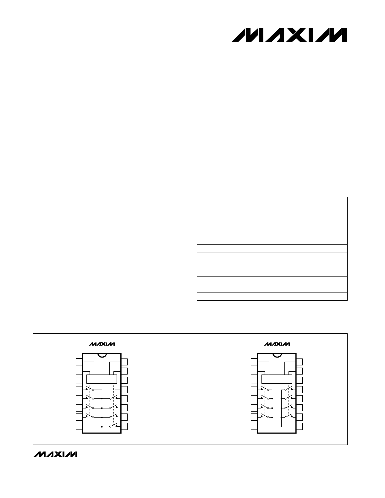
__________________________________________________________Pin Configurations
TOP VIEW
MAX354
1
A0
2
EN
LOGIC
3
V-
NO1
4
NO2
5
NO3
6
NO4
7
COM
8
DIP/SO
________________________________________________________________
16
A1
A2
15
GND
14
V+
13
12
NO5
NO6
11
NO7
10
NO8
9
A0
EN
VNO1A
NO2A
NO3A
NO4A
COMA
MAX355
1
2
LOGIC
3
4
5
6
7
8
DIP/SO
16
15
14
13
12
11
10
9
Maxim Integrated Products
A1
GND
V+
NO1B
NO2B
NO3B
NO4B
COMB
1
For free samples & the latest literature: http://www.maxim-ic.com, or phone 1-800-998-8800
Fault-Protected Analog Multiplexers
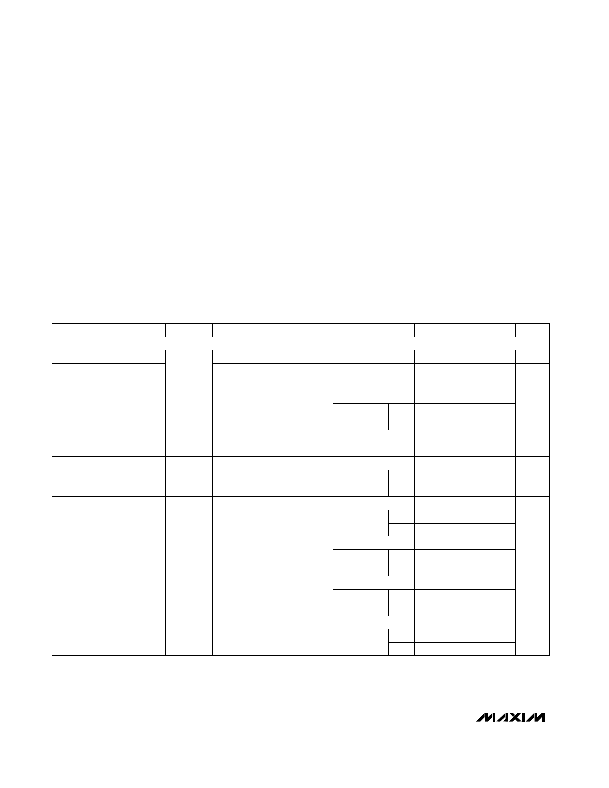
ABSOLUTE MAXIMUM RATINGS
(Voltages referenced to GND, unless otherwise noted.)
V+...........................................................................-0.3V to +44V
V-............................................................................+0.3V to -44V
V+ to V-...................................................................-0.3V to +44V
Digital Inputs.........................................(V+ + 0.3V) to (V- - 0.3V)
Input Overvoltage with Mux Power On
V+ = +15V ....................................................................... +25V
V- = -15V............................................................................-25V
Input Overvoltage with Mux Power Off
V+ = 0V.............................................................................+40V
V- = 0V...............................................................................-40V
Continuous Current into Any Terminal .............................±30mA
Stresses beyond those listed under “Absolute Maximum Ratings” may cause permanent damage to the device. These are stress ratings only, and functional
operation of the device at these or any other conditions beyond those indicated in the operational sections of the specifications is not implied. Exposure to
absolute maximum rating conditions for extended periods may affect device reliability.
ELECTRICAL CHARACTERISTICS
MAX354/MAX355
(V+ = +15V, V- = -15V, GND = 0V, VAH= V
= 2.4V, VAL= V
ENH
SWITCH
Analog Signal Range
Fault-Free Analog
Signal Range
On-Resistance
(Note 2)
On-Resistance Matching
Between Channels
NO-Off Leakage Current
(Note 4)
COM-Off Leakage Current
(Note 4)
V
COM
R
ON
∆R
I
NO(OFF)
I
COM(OFF)
(Note 1)
, V
NO
V+ = +15V, V- = -15V (Note 1)
INO= 1.0mA, V
INO= 1.0mA, V
ON
(Note 3)
V
COM
±
= ±10V,
VNO= ±10V,
VEN= 0V
V
V
COM
NO
±
= ±10V,
= ±10V,
VEN= 0V
= ±10V,
V
COM
NO
±
= ±10V,
V
COM
COM
VEN= 0V
V
= ±10V,
COM
V
COM-On Leakage Current
(Note 4)
I
COM(ON)
= ±10V,
NO
sequence each
switch on
Peak Current into Any Terminal........................................±50mA
Continuous Power Dissipation (T
= +70°C)
A
Plastic DIP (derate 10.53mW/°C above +70°C) ...........842mW
Wide SO (derate 9.52mW/°C above +70°C)................ 762mW
CERDIP (derate 10.00mW/°C above +70°C) ...............800mW
Operating Temperature Ranges
MAX35_C_ _ ........................................................0°C to +70°C
MAX35_E_ _......................................................-40°C to +85°C
MAX35_M_ _...................................................-55°C to +125°C
Storage Temperature Range.............................-65°C to +150°C
Lead Temperature (soldering, 10sec)............................ +300°C
= 0.8V, TA= T
ENL
MIN
to T
, unless otherwise noted.)
MAX
CONDITIONS
-12 12
285 350
450
500
712
15
= ±10V
= ±10V
MAX354
MAX355
MAX354
MAX355
TA= +25°C
TA= T
MIN
to T
MAX
TA= +25°C
TA= T
MIN
TA= +25°C
TA= T
MIN
to T
MAX
TA= +25°C
TA= T
MIN
to T
MAX
TA= +25°C
TA= T
MIN
to T
MAX
TA= +25°C
TA= T
MIN
to T
MAX
TA= +25°C
TA= T
MIN
to T
MAX
to T
C, E
M
MAX
C, E
M
C, E
M
C, E
M
C, E
M
C, E
M
-0.5 0.01 0.5
-5.0 5.0
-50 50
-0.5 0.02 0.5
-25 25
-100 100
-0.5 0.02 0.5
-15 15
-50 50
-0.5 0.02 0.5
-30 30
-200 200
-0.5 0.02 0.5
-15 15
-100 100
UNITSMIN TYP MAXSYMBOLPARAMETER
V(V+ - 40) (V- + 40)
V
Ω
Ω
nA
nA
nA
2 _______________________________________________________________________________________
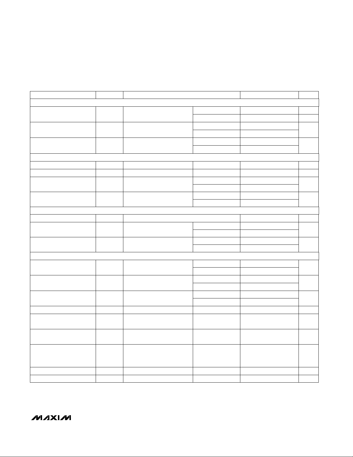
Fault-Protected Analog Multiplexers
ELECTRICAL CHARACTERISTICS (continued)
(V+ = +15V, V- = -15V, GND = 0V, VAH= V
FAULT
Output Leakage Current
(with Overvoltage)
Input Leakage Current
(with Overvoltage)
Input Leakage Current
(with Power Supplies Off)
DIGITAL LOGIC INPUT
Logic High Input Voltage
Logic Low Input Voltage
Input Current with
Input Voltage High
Input Current with
Input Voltage Low
A_H
A_L
I
A_H
I
A_L
, V
, V
, I
, I
ENH
ENL
ENH
ENL
SUPPLY
I+Positive Supply Current
I-Negative Supply Current
DYNAMIC
Transition Time
Enable Turn-On Time
Enable Turn-Off Time
Break-Before-Make Interval
Charge Injection
Off Isolation
t
TRANS
t
ON(EN)
t
OFF(EN)
OPEN
CTE
ISO
= 2.4V, VAL= V
ENH
= 0.8V, TA= T
ENL
CONDITIONS
VD= 0V,
analog overvoltage = ±33V
VIN= ±25V, VO= ±10V
VIN= ±25V, VEN= VO= 0V,
VA0= VA1= VA2= 0V or 5V
VA= VEN= 2.4V µA
VEN= VA= 5V
VEN= VA= 0V
Figure1
Figure 2
Figure 2
Figure 3
CL= 10nF, VS= 0V, RS= 0Ω,
Figure 4
VEN= 0V, RL= 1kΩ, f = 100kHz,
Figure 5
MIN
TA= +25°C
TA= T
MIN
TA= +25°C
TA= T
MIN
TA= +25°C
TA= T
MIN
TA= T
MIN
MIN
TA= +25°C
TA= T
MIN
TA= +25°C
TA= T
MIN
TA= +25°C
TA= T
MIN
TA= +25°C
TA= T
MIN
TA= +25°C
TA= T
MIN
TA= +25°C
TA= T
MIN
TA= +25°C
TA= T
MIN
TA= +25°C
TA= +25°C
TA= +25°C
to T
, unless otherwise noted.)
MAX
to T
MAX
-0.1 0.001 0.1
to T
MAX
-2 2
-0.1 0.001 0.1
to T
to T
to T
MAX
MAX
MAX
-2 2
-1 1
to T
MAX
-5 5
-1 1
to T
MAX
-5 5
-300 300
to T
MAX
-500 500
-1 1
to T
to T
to T
to T
MAX
MAX
MAX
MAX
-100 100
0.8V
180 250
400
160 250
400
80 200
300
MAX354/MAX355
UNITSMIN TYP MAXSYMBOLPARAMETER
nA-5 0.01 5
µA-2 2
µA
µA
V2.4V
VTA= T
µAVA= VEN= 0.8V
V±4.5 ±18Power-Supply Range
µA
µA
ns
ns
ns
ns50 100t
pC80V
dB100V
VEN= 2.4V, f = 100kHz,
Crosstalk Between Channels dB92
V
CT
V
GEN
= 1V
, RL= 1kΩ,
p-p
TA= +25°C
Figure 6
Logic Input Capacitance f = 1MHz, Figure 7 TA= +25°C
NO-Off Capacitance
IN
NO(OFF)
f = 1MHz, VEN= VD= 0V
TA= +25°C
_______________________________________________________________________________________ 3
pF
pF2.5C
pF1.6C
Fault-Protected Analog Multiplexers
ELECTRICAL CHARACTERISTICS (continued)
(V+ = +15V, V- = -15V, GND = 0V, VAH= V
= 2.4V, VAL= V
ENH
= 0.8V, TA= T
ENL
MIN
to T
, unless otherwise noted.)
MAX
CONDITIONS
DYNAMIC (cont’d)
COM-Off Capacitance pF
COM-On Capacitance pF
Setting Time (Note 5)
C
COM(OFF)
C
COM(ON)
t
SETT
f = 1MHz, Figure 7,
VEN= VD= 0V
f = 1MHz, Figure 7,
VEN= VD= 0V
0.1%
0.01%
MAX354
MAX355
MAX354
MAX355
TA= +25°C
TA= +25°C
TA= +25°C
11
5
28
14
1
2.5
Note 1: When the analog signal exceeds +13.5V or -13.5V, the blocking action of Maxim’s gate structure goes into operation. Only
leakage currents flow, and the channel on-resistance rises to infinity (see
Typical Operating Characteristics
).
Note 2: Electrical characteristics such as on-resistance will change when power supplies other than ±15V are used.
Note 3: ∆R
MAX354/MAX355
ON
= R
ON(MAX)
- R
ON(MIN)
Note 4: Leakage parameters are 100% tested at maximum rated hot operating temperature, and guaranteed by correlation at +25°C.
Note 5: Guaranteed by design.
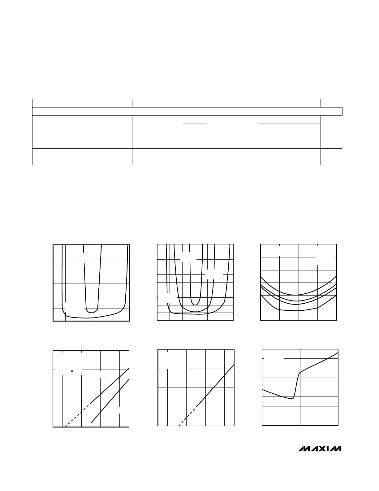
__________________________________________Typical Operating Characteristics
(TA = +25°C, unless otherwise noted.)
ON-RESISTANCE vs. ANALOG VOLTAGE
100
10
1
(MΩ)
0.1
ON
R
0.01
0.001
0.0001
-15 15
V+ = +5V
V- = -5V
V+ = +15V
V- = -15V
-10 -5 10
0
5
ANALOG VOLTAGE (V)
OFF LEAKAGE vs. TEMPERATURE
100
V+ = +15V
V- = -15V
= ±10V
V
NO_
10
1
OFF LEAKAGE (nA)
0.1
0.01
= 10V
V
COM_
-75 75 100 125
-50 -25 50
0
TEMPERATURE (°C)
I
COM(OFF)
25
I
NO(OFF)
2000
1800
MAX354/5-1a
1600
1400
1200
(Ω)
1000
ON
R
MAX354-3
ON LEAKAGE (nA)
0.01
ON-RESISTANCE vs. ANALOG VOLTAGE
800
V+ = +15V
600
V- = -15V
400
200
0
-15 15
-10 -5 10
ANALOG VOLTAGE (V)
ON LEAKAGE vs. TEMPERATURE
100
V+ = +15V
V- = -15V
= ±10V
V
COM_
10
1
0.1
-75 75 100 125
-50 -25 50
V+ = +5V
V- = -5V
V+ = +10V
V- = -10V
0
5
0
25
TEMPERATURE (°C)
700
MAX354/5-1b
600
500
(Ω)
400
ON
R
300
200
100
-10 -5 10
200
MAX354-4
150
100
50
(pC)
0
j
Q
-50
-100
-150
-200
-10 5 10
4 _______________________________________________________________________________________
ON-RESISTANCE vs.
AND TEMPERATURE
V
COM
V+ = +15V
V- = -15V
0
V
COM
CHARGE INJECTION vs. V
V+ = +15V
V- = -15V
-5
V
COM
A: +125°C
B: +85°C
C: +70°C
D: +25°C
5
(V)
0
(V)
UNITSMIN TYP MAXSYMBOLPARAMETER
µs
MAX354/5-2
A
B
C
D
COM
MAX354-5

Fault-Protected Analog Multiplexers
____________________________Typical Operating Characteristics (continued)
(TA = +25°C, unless otherwise noted.)
SUPPLY CURRENT vs. TEMPERATURE
1000
V+ = +15V
V- = -15V
= +5V
V
EN
100
10
I+, I- (µA)
1
0.1
-75 75 100 125
-50 -25 50
0
25
TEMPERATURE (°C)
I+ (VA_ = 5V)
I+ (VA_ = 0V)
I-
MAX354-6
FAULT CURRENT vs. FAULT VOLTAGE
10m
1m
100µ
10µ
1µ
100m
10n
FAULT CURRENT (A)
1n
100p
10p
-50
-70 -10 10 30 50 70
-30
V+ = V- = 0V
V+ = +15V
V- = -15V
FAULT VOLTAGE (V)
______________________________________________________________Pin Description
MAX354/MAX355
PIN
FUNCTIONNAME
MAX355MAX354
—
—
1, 16
Address Logic InputsA0, A2, A11, 15, 16
Address Logic InputsA0, A1
Enable Logic Input. See truth tables.EN22
Negative Supply Voltage Input. Connect to GND for single-supply operation.V-33
Analog Inputs—bidirectionalNO1–NO4—4–7
Analog Inputs—bidirectional “A” switchNO1A–NO4A4–7—
Analog Output—bidirectionalCOM—8
Analog Outputs—bidirectionalCOMA, COMB8, 9—
Analog Inputs—bidirectionalNO8–NO5—9–12
Analog Inputs—bidirectional “B” switchNO4B–NO1B10–13—
Positive Supply Voltage InputV+1413
GroundGND1514
Note: Analog inputs and outputs are electrically identical and completely interchangeable.
_______________________________________________________________________________________ 5

Fault-Protected Analog Multiplexers
______________________________________________Test Circuits/Timing Diagrams
+15V
V+
NO2-NO7
-15V
V+
NO1A-NO4A
-15V
V-
COMB
V-
NO1
NO8
COM
NO1B
NO4B
300Ω
300Ω
+10V
-10V
+10V
-10V
35pF
35pF
LOGIC
V
OUT
V
OUT
INPUT
V
EN
SWITCH
OUTPUT
V
OUT
+3V
0V
V
NO1
0V
V
NO8
t
TRANS
ON
50%
90%
tR < 20ns
< 20ns
t
F
90%
t
TRANS
A2
A1
A0
MAX354
V
EN
EN
50Ω
MAX354/MAX355
50Ω
GND
+15V
A1
A0
V
EN
MAX355
EN
GND
Figure 1. Transition Time
+15V
GND
GND
V+
MAX354
+15V
V+
NO1A–NO4A
NO2B–NO4B,
MAX355
NO1
NO2–NO8
COM
V-
-15V
NO1B
COMA
COMB
V-
-15V
+10V
V
OUT
1k
+10V
1k
35pF
35pF
V
OUT
LOGIC
INPUT
V
SWITCH
OUTPUT
V
EN
OUT
+3V
t
ON(EN)
50%
0V
0V
90%
V
EN
EN
A0
A1
A2
50Ω
V
EN
EN
50Ω
A0
A1
Figure 2. Enable Switching Time
6 _______________________________________________________________________________________
tR < 20ns
< 20ns
t
F
10%
t
OFF(EN)

Fault-Protected Analog Multiplexers
_________________________________Test Circuits/Timing Diagrams (continued)
+15V
V
GND
EN
V+
MAX354
NO
EN
A0
A1
A2
GND
NO1–NO8
COM
V-
-15V
+15V
V+
MAX354
300Ω
V-
-15V
COM
+10V
V
OUT
35pF
V
OUT
CL = 1000nF
LOGIC
INPUT
V
EN
V
OUT
+3V
0V
+3V
LOGIC
INPUT
0V
V
A
+5V
SWITCH
OUTPUT
V
OUT
0V
IS THE MEASURED VOLTAGE DUE TO CHARGE TRANSFER
∆V
OUT
ERROR V
V
WHEN THE CHANNEL TURNS OFF.
CTE
= ∆V
CTE
OUT x CL
50%
80%
ONOFF OFF
t
OPEN
tR < 20ns
< 20ns
t
F
∆V
OUT
V
EN
+2.4V
V
A
EN
A0
A1
A2
50Ω
Figure 3. Break-Before-Make Interval
R
S
V
S
CHANNEL
SELECT
MAX354/MAX355
Figure 4. Charge Injection
_______________________________________________________________________________________ 7

Fault-Protected Analog Multiplexers
_________________________________Test Circuits/Timing Diagrams (continued)
10nF
+15V
10nF
+15V
V
IN
R
S
= 50Ω
NO1
NO8
V+
R = 1kΩ
MAX354
A0
A1
A2
EN
GND
MAX354/MAX355
10nF
COM
V-
-15V
OFF ISOLATION = 20log
V
OUT
R
L
1k
V
OUT
V
IN
R
= 50Ω
G
Figure 5. Off Isolation Figure 6. Crosstalk
+15V
GND
V+
MAX354
EN
V-
-15V
NO1
NO8
COM
1MHz
CAPACITANCE
ANALYZER
f = 1MHz
CHANNEL
SELECT
A2
A1
A0
GND
V+
MAX354
EN
10nF
COM
R
V-
-15V
CROSSTALK = 20log
1k
V
OUT
L
V
OUT
V
IN
NO1
V
IN
NO2
NO8
A0
A1
A2
Figure 7. NO/COM Capacitance
_______________Detailed Description
1.5V below the supply rails and maintains the correct
polarity. There are no glitches or polarity reversals
Fault-Protection Circuitry
Maxim’s MAX354/MAX355 are fully fault protected for
continuous input voltages up to ±40V, whether or not
the V+ and V- power supplies are present. These
devices use a “series FET” protection scheme that not
only protects the multiplexer output from overvoltage,
but also limits the input current to sub-microamp levels.
When signal voltages exceed or are within approximately 1.5V of the supply rails, on-resistance increases. This greater on-resistance limits fault currents and
output voltage, protecting sensitive circuits and components. The protected output clamps at approximately
8 _______________________________________________________________________________________
going into or coming out of a fault condition.
Figures 8 and 9 show how the series FET circuit protects
against overvoltage conditions. When power is off, the
gates of all three FETs are at ground. With a -25V input,
N-channel FET Q1 is turned on by the +25V gate-tosource voltage. The P-channel device (Q2), however,
has +25V V
and is turned off, thereby preventing the
GS
input signal from reaching the output. If the input voltage is +25V, Q1 has a negative VGS, which turns it off.
Similarly, only sub-microamp leakage currents can flow
from the output back to the input, since any voltage will
turn off either Q1 or Q2.

Fault-Protected Analog Multiplexers
Figure 10 shows the condition of an off channel with V+
and V- present. As with Figures 8 and 9, either an Nchannel or a P-channel device will be off for any input
voltage from -40V to +40V. The leakage current with
negative overvoltages will immediately drop to a few
nanoamps at +25°C. For positive overvoltages, that
fault current will initially be 10µA or 20µA, decaying
over a few seconds to the nanoamp level. The time
constant of this decay is caused by the discharge of
stored charge from internal nodes and does not compromise the fault-protection scheme.
Figure 11 shows the condition of the on channel with
V+ and V- present. With input voltages less than ±10V,
all three FETs are on and the input signal appears at
the output. If the input voltage exceeds V+ minus the
N-channel threshold voltage (VTN), the N-channel FET
will turn off. For voltages more negative than V- minus
the P-channel threshold (VTP), the P-channel device will
turn off. Since VTNis typically 1.5V and VTPis typically
3V, the multiplexer’s output swing is limited to about -12V
to +13.5V with ±15V supplies.
Switching Characteristics
and Charge Injection
Table 1 shows typical charge injection levels versus
power-supply voltages and analog input voltage. The
charge injection that occurs during switching creates a
voltage transient whose magnitude is inversely proportional to the capacitance on the multiplexer output.
Table 1. MAX354 Charge Injection
Supply Voltage Analog Input Level Injected Charge
+2V
±5V
0V
-2V
+5V
±10V
0V
-5V
+10V
±15V
0V
-10V
Test Conditions: CL, = 1000pF on mux output; the tabulated
analog input level is applied to channel 1; channels 2–8 inputs
are open circuited. EN = +5V, V
= VA2= 0V, VOis toggled at
A1
a 2kHz rate between 0V and 3V. +100pC of charge creates a
+100mV step when injected into a 1000pF load capacitance.
52pC
35pC
16pC
105pC
65pC
25pC
180pC
80pC
15pC
MAX354/MAX355
-25V
OVERVOLTAGE
N-CHANNEL MOSFET
IS TURNED ON
BECAUSE V
GS
= +25V
Q1
D
S
G
P-CHANNEL
MOSFET IS OFF
-25V
S
Q2
D
G
Q3
D
S
G
Figure 8. -25V Overvoltage with Multiplexer Power Off
+15V-15V -15V
-25V
OVERVOLTAGE
N-CHANNEL MOSFET
IS TURNED ON
BECAUSE V
GS
= +10V
Q1
-15V FROM
DRIVERS
P-CHANNEL
MOSFET IS OFF
Q2 Q3
+15V FROM
DRIVERS
+25V FORCED
ON COMMON
OUTPUT LINE BY
EXTERNAL CIRCUITRY
N-CHANNEL
MOSFET IS OFF
Figure 10. -25V Overvoltage on an Off Channel with
Multiplexer Power Supply On
_______________________________________________________________________________________ 9
+25V
OVERVOLTAGE
N-CHANNEL MOSFET
IS TURNED OFF
BECAUSE V
GS
= -25V
Q1
D
S
G
Q2
D
S
G
Q3
D
S
G
Figure 9. +25V Overvoltage with Multiplexer Power Off
+15V-15V -15V
+25V
OVERVOLTAGE
N-CHANNEL MOSFET
IS TURNED OFF
BECAUSE V
GS
= -10V
Q1
V
+15V FROM
DRIVERS
TN
13.5V
= 1.5V
-15V FROM
DRIVERS
Q2 Q3
13.5V
OUTPUT
N-CHANNEL
MOSFET IS ON
Figure 11. +25V Overvoltage Input to the On Channel

Fault-Protected Analog Multiplexers
The channel-to-channel switching time is typically
180ns, with about 100ns of break-before-make delay.
This 100ns break-before-make delay prevents the
input-to-input short that would occur if two input channels were simultaneously connected to the output. In a
typical data acquisition system, the dominant delay is
not the switching time of the multiplexer, but is the settling time of the amplifiers and S/H. Another limiting factor is the RC time constant of the multiplexer RONplus
the signal source impedance multiplied by the load
capacitance on the output of the multiplexer. Even with
low signal source impedances, 100pF of capacitance
on the multiplexer output will approximately double the
settling time to 0.01% accuracy.
Operation with Supply Voltages
MAX354/MAX355
The main effect of supply voltages other than ±15V is
the reduction in output signal range. The MAX354 limits
the output voltage to about 1.5V below V+ and about
3V above V-. In other words, the output swing is limited
to +3.5V to -2V when operating from ±5V. The
Operating Characteristics
power supplies. Maxim tests and guarantees the
MAX354/MAX355 for operation from ±4.5V to ±18V
supplies. The switching delays are increased by about
a factor of 2 at ±5V, but break-before-make action is
preserved.
The MAX354/MAX355 can operate with a single +4.5V
to +30V supply, as well as asymmetrical power supplies such as +15V and -5V. The digital threshold
remains approximately 1.6V above the GND pin, and
the analog characteristics, such as RON, are determined by the total voltage difference between V+ and
V-. Connect V- to 0V when operating with a +4.5V to
+30V single supply.
The MAX354 digital threshold is relatively independent
of the power-supply voltages, going from 1.6V typical
when V+ is 15V to 1.5V typical when V+ is 5V. This
means that the MAX354/MAX355 operate with standard
TTL-logic levels, even with ±5V power supplies. In all
cases, the threshold of the enable (EN) pin is the same
as the other logic inputs.
show RONfor +15V and ±5V
Other than ±15V
Typical
Digital Interface Levels
The typical digital threshold of both the address lines
and the enable pin is 1.6V, with a temperature coefficient of about -3mV/°C. This ensures compatibility with
0.8V to 2.4V TTL-logic swings over the entire temperature range. The digital threshold is relatively independent of the supply voltages, moving from 1.6V typical to
1.5V typical as the power supplies are reduced from
±15V to ±5V. In all cases, the digital threshold is referenced to the GND pin.
The digital inputs can also be driven with CMOS-logic
levels swinging from either V+ to V- or from V+ to
ground. The digital input current is just a few nanoamps
of leakage at all input voltage levels, with a guaranteed
maximum of 1µA.
Operation as a Demultiplexer
The MAX354/MAX355 function as demultiplexers where
the input is applied to the output pin, and the input pins
are used as outputs. The MAX354/MAX355 provide
both break-before-make action and full fault protection
when operated as demultiplexers, unlike earlier generations of fault-protected muxes.
Channel-to-Channel Crosstalk,
Off-Isolation, and Digital Feedthrough
At DC and low frequencies the channel-to-channel
crosstalk is caused by variations in output leakage currents as the off-channel input voltages are varied. The
MAX354 output leakage varies only a few picoamps as
all seven off inputs are toggled from -10V to +10V. The
output voltage change depends on the impedance
level at the MAX354 output, which is RONplus the input
signal source resistance in most cases, since the load
driven by the MAX354 is usually high impedance. For a
signal source impedance of 10kΩ or lower, the DC
crosstalk exceeds 120dB.
Tables 2a and 2b show typical AC crosstalk and offisolation performance. Digital feedthrough is masked
by the analog charge injection when the output is
enabled. When the output is disabled, the digital
feedthrough is virtually unmeasureable, since the digital pins are physically isolated from the analog section
by the GND and V- pins. The ground plane formed by
these lines is continued onto the MAX354/MAX355 die
to provide over 100dB isolation between the digital and
analog sections.
10 ______________________________________________________________________________________

Fault-Protected Analog Multiplexers
Table 2a. Typical Off-Isolation Rejection
Ratio
Frequency 100kHz 1MHz
One Channel Driven 100dB 80dB
Test Conditions: V
= 1.5kΩ between OUT and ground, EN = 0V.
R
L
= 20Vp-p at the tabulated frequency,
IN
V
= 20log —————
ISO
20Vp-p
V
OUT
(p-p)
Table 2b. Typical Crosstalk Rejection Ratio
Frequency 100kHz 1MHz
RL= 1.5kΩ 92dB 72dB
RL= 10kΩ 76dB 56dB
Test Conditions: Specified RLconnected from OUT to ground,
EN = +5V, A
at the tabulated frequency is applied to Channel 2. All other
channels are open circuited. Similar crosstalk rejection can be
observed between any two channels.
= A1= A2= +5V (Channel 1 selected). 20Vp-p
0
__________________________________________Functional Diagrams/Truth Tables
MAX354
NO1
NO2
NO3
NO4
NO5
NO6
NO7
NO8
V+ V- GND
DECODERS / DRIVERS
A0 A1 A2 EN
COM
MAX354
A0A1A2 EN ON SWITCH
X
X
X
0
NONE
0
0
0
1
0
0
1
1
0
1
0
1
0
1
1
1
1
0
0
1
1
0
1
1
1
1
0
1
1
1
1
1
LOGIC "O" VAL ≤ +0.8V, LOGIC "1" VAH ≥ +2.4V
1
2
3
4
5
6
7
8
MAX354/MAX355
MAX355
NO1A
NO2A
NO3A
NO4A
NO1B
NO2B
NO3B
NO4B
V+ V- GND
DECODERS / DRIVERS
A0 A1 EN
COMA
COMB
X
0
0
1
1
LOGIC "O" VAL ≤ +0.8V, LOGIC "1" VAH ≥ +2.4V
MAX355
A0A1 EN ON SWITCH
X
0
NONE
0
1
1
1
0
1
1
1
1
2
3
4
______________________________________________________________________________________ 11

Fault-Protected Analog Multiplexers
__________________________________________________________Chip Topographies
MAX354
EN
V-
N01
MAX354/MAX355
N02
N03
N04 COM N08 N07
A0 A1 A2 GND
0.115"
(2.92mm)
EN
V-
V+
N05
0.130"
(3.30mm)
N06
N.C.
N01A
N02A
N03A
N04A
TRANSISTOR COUNT: 256
SUBSTRATE CONNECTED TO V+
MAX355
A0 A1 GND
V+
N.C.
N01B
0.130"
(3.30mm)
N02B
N03B
COMA COMB N04B
0.115"
(2.92mm)
Maxim cannot assume responsibility for use of any circuitry other than circuitry entirely embodied in a Maxim product. No circuit patent licenses are
implied. Maxim reserves the right to change the circuitry and specifications without notice at any time.
12
__________________Maxim Integrated Products, 120 San Gabriel Drive, Sunnyvale, CA 94086 (408) 737-7600
© 1996 Maxim Integrated Products Printed USA is a registered trademark of Maxim Integrated Products.
 Loading...