

For free samples & the latest literature: http://www.maxim-ic.com, or phone 1-800-998-8800.
For small orders, phone 1-800-835-8769.
General Description
The MAX3510 is a programmable power amplifier for
use in CATV upstream applications. The device outputs
up to 64dBmV (continuous wave) through a 2:1 (voltage
ratio) transformer. It features variable gain controlled by
a 3-wire digital serial bus. Gain control is available in
1dB steps. The device operates over a frequency
range of 5MHz to 65MHz.
The MAX3510 offers a transmit-disable mode, which
places the device in a high-isolation state for use
between bursts in TDMA systems. In this mode the output stage is shut off, minimizing output noise. When
entering and leaving transmit-disable mode, transients
are kept to 7mV nominal at full gain. In addition, supply
current is reduced to 25mA.
Two power-down modes are available. Software-shutdown
mode permits power-down of all analog circuitry while
maintaining the programmed gain setting. Shutdown
mode disables all circuitry and reduces current consumption to less than 10µA.
The MAX3510 is available in a 20-pin QSOP package
for the extended-industrial temperature range (-40°C to
+85°C).
Applications
Cable Modems Telephony over Cable
CATV Set-Top Box CATV Status Monitor
Features
♦ Ultra-Low Power-Up/Down Transients,
7mV Typical at 59dBmV Output
♦ Single +5V Supply
♦ Output Level Ranges from <8dBmV to 64dBmV
♦ Gain Programmable in 1dB Steps
♦ Low Transmit Output Noise Floor: -47dBmV
(160kHz BW)
♦ Low Transmit-Disable Output Noise: -70dBmV
♦ Two Power-Down Modes
MAX3510
Upstream CATV Amplifier
________________________________________________________________
Maxim Integrated Products
1
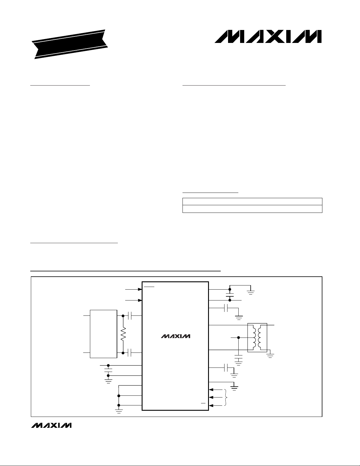
Typical Operating Circuit
19-1398; Rev 2; 8/99
PART
MAX3510EEP -40°C to +85°C
TEMP. RANGE PIN-PACKAGE
20 QSOP
EVALUATION KIT MANUAL
FOLLOWS DATA SHEET
Pin Configuration appears at end of data sheet.
Ordering Information
12
SHDN
18
TXEN
5
VIN+
+
INPUT
CONTROL
LOGIC
0.001µF
ANTI-ALIAS
FILTER
MAX3510
0.001µF
6
VIN-
2
1
V
CC
4
GND1
3
GND
7
GND
1
GND
–
+5V
0.1µF
GND2
V
CC
CEXT1
VOUT+
VOUT-
CEXT2
N.C.
GND
SCLK
SDA
20
19
2
17
16
15
14
13
11
10
9
8
CS
0.0033µF
+5V
0.1µF
0.1µF
CONTROL
LOGIC
+5V
2:1
0.1µF
OUTPUT
MAX3510
Upstream CATV Amplifier
2 _______________________________________________________________________________________
ABSOLUTE MAXIMUM RATINGS
DC ELECTRICAL CHARACTERISTICS
(VCC= +4.75V to +5.25V, TXEN = SHDN = high, D7 = 1, TA = -40°C to +85°C, unless otherwise noted. No input signal applied.
Typical parameters are at T
A
= +25°C.)
Stresses beyond those listed under “Absolute Maximum Ratings” may cause permanent damage to the device. These are stress ratings only, and functional
operation of the device at these or any other conditions beyond those indicated in the operational sections of the specifications is not implied. Exposure to
absolute maximum rating conditions for extended periods may affect device reliability.
VCC(VCC1, VCC2), VOUT+, VOUT- ................... -0.5V to +10.0V
Input Voltage Levels (all inputs),
CEXT1, CEXT2.........................................-0.3V to (V
CC
+ 0.3V)
Continuous Input Voltage (VIN+, VIN-)...............................2Vp-p
Continuous Current (VOUT+, VOUT-).................................80mA
Continuous Power Dissipation (T
A
= +70°C)
20-Pin QSOP (derate at 12.3mW/°C above +70°C)....1067mW
Operating Temperature Range ...........................-40°C to +85°C
Junction Temperature......................................................+150°C
Storage Temperature Range .............................-65°C to +165°C
Lead Temperature (soldering, 10sec) .............................+300°C
TXEN = low
TXEN = low, D7 = 0
SHDN = low, TXEN = low
CONDITIONS
mA26 30I
CC
Supply Current Transmit-Disable
Mode
mA109 126I
CC
V4.75 5.25V
CC
Supply Voltage
Supply Current Transmit Mode
µA-100I
BIASL
Input Low Current
µA100I
BIASH
Input High Current
mA1.4 2.0I
CC
Supply Current SoftwareShutdown Mode
µA110I
CC
Supply Current Shutdown Mode
V2.0V
INH
Input High Voltage
V0.8V
INL
Input Low Voltage
UNITSMIN TYP MAXSYMBOLPARAMETER
AC ELECTRICAL CHARACTERISTICS
(VCC= +4.75V to +5.25V, TXEN = SHDN = high, D7 = 1, VIN= 34dBmV differential, output impedance = 75Ω through a 2:1 transformer, T
A
= -40°C to +85°C, unless otherwise noted. Typical parameters are at TA= +25°C.)
V
OUT
= 60dBmV, fIN= 42MHz (Notes 1, 2)
V
OUT
= 60dBmV, fIN= 65MHz (Notes 1, 2)
dB
-0.9 -1
-1.6 -1.8
AV= 26dB, 42MHz (Note 1)
V
OUT
= 60dBmV, -3dB (Note 1)
CONDITIONS
Gain Rolloff
dBm18.0 20.0P1dB1dB Compression Point
MHz84 100f
3dB
Bandwidth
UNITSMIN TYP MAXSYMBOLPARAMETER
-26
Gain control word = 1,
TA= -40°C to +85°C
26
Gain control word = 63,
TA= 0°C to +85°C
27
Gain control word = 63,
TA= -40°C to 0°C
Gain control word = 50,
TA= -40°C to +85°C
fIN= 5MHz
to 42MHz
16.7 20.4
dBA
V
Voltage Gain
dB
0.7 1 1.3
Output Step Size
AV= -26dB to +27dB,
T
A
= -40°C to +85°C
f
IN
= 5MHz to 42MHz
AV= -26dB to +26dB,
TA= -40°C to 0°C
0.65 1 1.3
fIN= 10MHz
dBc
MAX3510
Upstream CATV Amplifier
_______________________________________________________________________________________ 3
BW = 160kHz, AV= -26dB (Note 1)
BW = 160kHz, AV= 26dB (Note 1)
fIN= 5MHz to 65MHz
(Note 1)
fIN= 5MHz to 65MHz, single-ended,
TA= +25°C (Note 1)
CONDITIONS
dBc
47 -46
-78
Transmit Mode Noise
7.7 12.2
8.0 13.5
Z
IN
kΩ1.4 1.5Input Impedance
Ω75Z
OUT
Output Impedance
UNITSMIN TYP MAXSYMBOLPARAMETER
AC ELECTRICAL CHARACTERISTICS (continued)
(VCC= +4.75V to +5.25V, TXEN = SHDN = high, D7 = 1, VIN= 34dBmV differential, output impedance = 75Ω through a 2:1 transformer, T
A
= -40°C to +85°C, unless otherwise noted. Typical parameters are at TA= +25°C.)
Input tones at 40MHz and 40.2MHz,
VIN= 28dBmV/tone, V
OUT
= +54dBmV/tone,
TA= +25°C (Note 1)
fIN= 33MHz,
TA= -40°C to +85°C
-59 -53
-55 -50
dBc
-54 -50
2nd Harmonic Distortion
fIN= 22MHz,
TA= -40°C to +85°C
-54 -50
-58 -53
dBc
AV= 26dB, VINswept from 34dBmV to
38dBmV (Note 1)
dB0.1AM/AMAM to AM
AV= 26dB, VINswept from 34dBmV to
38dBmV (Note 1)
degrees1AM/PMAM to PM
HD2
fIN= 65MHz, V
OUT
= +59dBmV,
TA= +25°C (Note 1)
HD33rd Harmonic Distortion
fIN= 65MHz, V
OUT
= +59dBmV,
T
A
= +25°C (Note 1)
-49 -44
IM3Two-Tone Third-Order Distortion dBc
dB
8.9 13.9
R
L
Output Return Loss in Transmit
Mode
8.7 13.5
TXEN = low,
fIN= 5MHz to 65MHz
(Note 1)
7.1 12.0
R
L
dB
Output Return Loss in
Transmit-Disable Mode
-56 -53
TA= 0°C
TA= +25°C
TA= +85°C
TA= 0°C
TA= +25°C
TA= +85°C
V
OUT
= +54dBmV
V
OUT
= +59dBmV
V
OUT
= +54dBmV
V
OUT
= +59dBmV
Input tones at 65MHz and 65.2MHz,
VIN= 28dBmV/tone, V
OUT
= 53dBmV/tone,
TA= +25°C (Note 1)
-54 -51
9.7 12.7
Gain = 2dB or lower, TA= +25°C (Note 1)
Gain = 26dB, TA= +25°C (Note 1)
mVp-p
0.7 3.7
737
TXEN Transient Step Size
dBmV
TXEN = low, BW = 160kHz,
AV= +26dB, fIN= 5MHz to 65MHz (Note 1)
dBmV-70
Transmit-Disable Mode Noise
Floor
TXEN low, gain control word = 61,
fIN= 65MHz
dB36 45
Isolation in Transmit-Disable
Mode
TXEN rise/fall time < 0.1µs, TA= +25°C (Note 1) µs3.2 5TXEN Transient Duration
MAX3510
Upstream CATV Amplifier
4 _______________________________________________________________________________________
Note 1: Guaranteed by design and characterization.
Note 2: Reference to 5MHz.
TIMING CHARACTERISTICS
(VCC= +4.75V to +5.25V, TXEN = SHDN = high, D7 = 1, TA = +25°C, unless otherwise noted.)
COMMENT
ns10t
SDAS
SDA to SCK Setup Time
ns20t
SENH
ns10t
SENS
CS to SCK Rise Setup Time
CS to SCK Rise Hold Time
ns50t
SCKL
SCK Pulse Width Low
ns20t
SDAH
SDA to SCK Hold Time
ns50t
DATAH
SDA Pulse Width High
ns50t
DATAL
SDA Pulse Width Low
ns50t
SCKH
SCK Pulse Width High
UNITSMIN TYP MAXSYMBOLPARAMETER
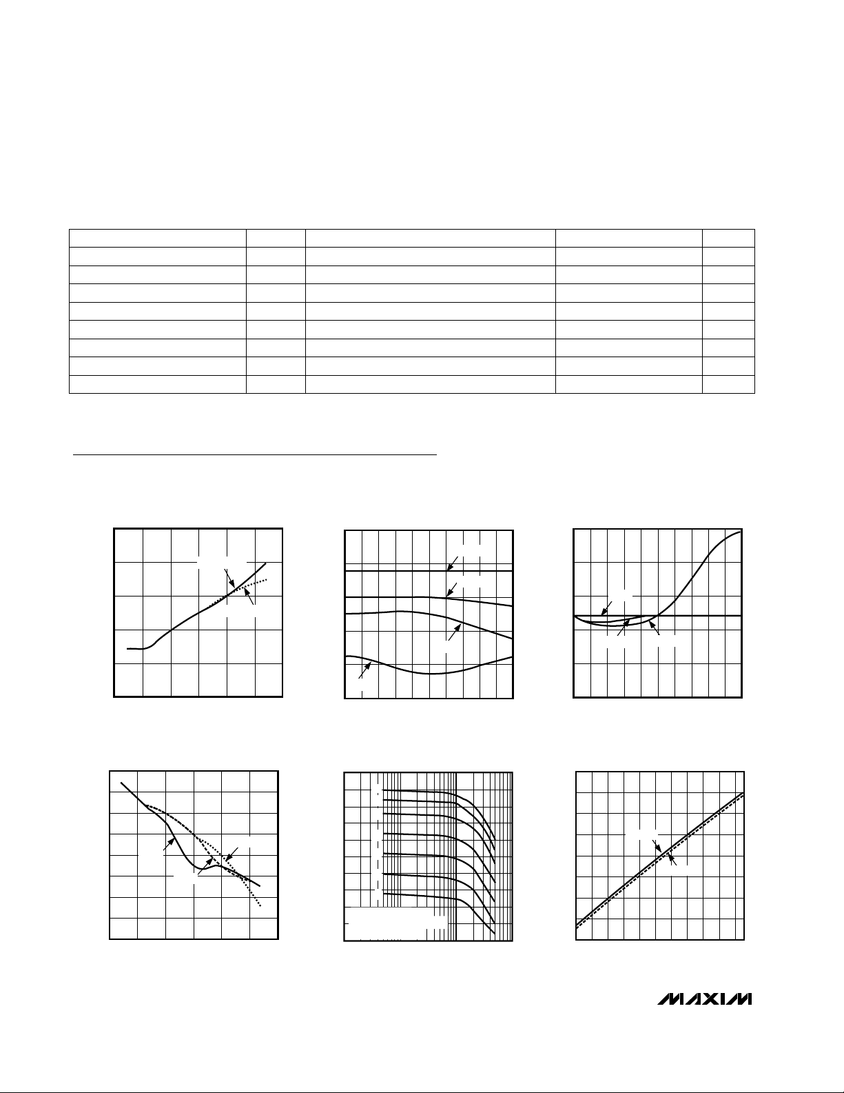
Typical Operating Characteristics
(VCC= +5V, VIN= +34dBmV, TXEN = SHDN = high, fIN= 20MHz, Z
LOAD
= 75Ω through a 2:1 transformer, TA= +25°C, unless
otherwise noted.)
102
104
108
106
110
112
-50 0-25 25 50 75 100
SUPPLY CURRENT vs. TEMPERATURE
MAX3510 toc01
TEMPERATURE (°C)
SUPPLY CURRENT (mA)
VCC = 5.25V
VCC = 4.75V
0
0.4
0.8
1.2
1.6
2.0
4.75 4.95 5.04.85 4.94.8 5.05 5.1 5.15 5.2 5.25
VOLTAGE GAIN vs. SUPPLY VOLTAGE
(GAIN STATE = 33)
MAX3510 toc02
SUPPLY VOLTAGE (V)
VOLTAGE GAIN (dB)
-40°C
0°C
+25°C
+85°C
26.6
26.8
4.75 4.95 5.04.85 4.94.8 5.05 5.1 5.15 5.2 5.25
VOLTAGE GAIN vs. SUPPLY VOLTAGE
(GAIN STATE = 60)
MAX3510 toc03
SUPPLY VOLTAGE (V)
VOLTAGE GAIN (dB)
-40°C
+25°C
+85°C
0
0.2
0.4
0.6
0.8
1.0
1.2
1.4
1.6
-50 0-25 25 50 75 100
VOLTAGE GAIN vs. TEMPERATURE
(GAIN STATE = 33)
MAX3510 toc04
TEMPERATURE (°C)
VOLTAGE GAIN (dB)
5.25V
5.0V
4.75V
40
-60
1 10 100 1000
VOLTAGE GAIN vs. FREQUENCY
-40
MAX3510 toc05
FREQUENCY (MHz)
VOLTAGE GAIN (dB)
-20
0
20
30
-50
-30
-10
10
G
F
E
D
C
B
A
A=63
B=57
C=48
D=36
E=24
F=12
G=6
GAIN CONTROL WORD:
-40
-30
30
-10
-20
0
10
20
40
0 121824630365448 6042
VOLTAGE GAIN vs. GAIN CONTROL WORD
MAX3510 toc06
GAIN CONTROL WORD (DECIMAL)
VOLTAGE GAIN (dB)
f = 5MHz
f = 40MHz

MAX3510
Upstream CATV Amplifier
_______________________________________________________________________________________
5
Typical Operating Characteristics (continued)
(V
CC
= +5V, VIN= +34dBmV, TXEN = SHDN = high, fIN= 20MHz, Z
LOAD
= 75Ω through a 2:1 transformer, TA= +25°C, unless
otherwise noted.)
VOLTAGE GAIN vs. GAIN CONTROL WORD
30
28
26
24
22
20
VOLTAGE GAIN (dB)
18
16
14
f = 5MHz
48 52 5450 56 58 60 62 64
GAIN CONTROL WORD (DECIMAL)
f = 40MHz
f = 60MHz
OUTPUT RETURN LOSS vs. FREQUENCY
0
MAX3510 toc07
GAIN STEP vs. GAIN CONTROL WORD
1.25
1.15
1.05
0.95
GAIN STEP (dB)
0.85
0.75
012186 24303642485460
TRANSMIT OUTPUT NOISE vs. GAIN
-20
OUTPUT IMPEDANCE
(75Ω REFERENCE)
GAIN CONTROL WORD (DECIMAL)
MAX3510 toc08
TRANSMIT-DISABLE
MODE
POWER-UP/POWER-DOWN
TRANSIENTS vs. OUTPUT LEVEL
100
5MHz
65MHz
TRANSMIT
MODE
MAX3510 toc10
4
8
TRANSMIT-DISABLE
MODE
12
RETURN LOSS (dB)
16
20
5453515 25 55 65 75 85 95 105
FREQUENCY (MHz)
TRANSMIT
MODE
2nd HARMONIC DISTORTION vs.
INPUT FREQUENCY AND OUTPUT LEVEL
-40
-45
-50
V
= 57dBmV
OUT
-55
-60
-65
-70
2nd HARMONIC DISTORTION (dBc)
-75
-80
02010 30 40 50 60 70
V
= 6dBmV
OUT
FREQUENCY (MHz)
V
OUT
-25
MAX3510 toc11
-30
-35
-40
OUTPUT NOISE (dBmV IN 160kHz)
-45
-50
-33
= 60dBmV
V
= 30dBmV
OUT
-9-15-27 -21 -3 93152127
GAIN (dB)
MAX3510 toc14
MAX3510 toc12
10
1
TRANSIENT LEVEL (mVp-p)
0.1
0403010 20 50 60
3rd HARMONIC DISTORTION vs.
INPUT FREQUENCY
-35
-40
-45
-50
-55
-60
-65
3rd HARMONIC DISTORTION (dBc)
-70
-75
02010 30 40 50 60 70
V
= 60dBmV
OUT
V
= 54dBmV
OUT
V
= 48dBmV
OUT
V
OUT
V
= 6dBmV
OUT
INPUT FREQUENCY (MHz)
MAX3510 toc13
OUTPUT LEVEL (dBmV)
MAX3510 toc15
= 24dBmV

MAX3510
Upstream CATV Amplifier
6 _______________________________________________________________________________________
Table 1. Reflection Coefficients (75Ω reference)
Pin Description
PIN
Ground PinsGND
1, 3,
7, 11
FUNCTIONNAME
Programmable-Gain Amplifier (PGA) +5V Supply. Bypass this pin to GND1 with a decoupling capacitor as
close to the part as possible.
VCC12
PGA RF Ground. As with all ground connections, maintain the shortest possible (low-inductance) length to
the ground plane.
GND14
Negative PGA Input. When not used, this port must be AC-coupled to ground. See VIN+.VIN-6
Serial-Interface Enable. TTL-compatible input. See
Serial Interface
section.
CS
8
Positive PGA Input. Along with VIN-, this port forms a high-impedance differential input to the PGA. Driving
this port differentially will increase the rejection of second-order distortion at low output levels.
VIN+5
Serial-Interface Clock. TTL-compatible input. See
Serial Interface
section.SCLK10
No ConnectionN.C.13
Shutdown. When this pin and TXEN (pin 18) are set low, all functions (including the serial interface) are disabled, leaving only leakage currents to flow.
SHDN
12
Negative Output. Along with VOUT+, this port forms a 300Ω impedance output. This port is matched to a
75Ω load using a 2:1 transformer.
VOUT-15
Transmit-Disable (Enable) Timing Capacitor. See
Ramp Generator
section.CEXT117
Positive Output. See VOUT-.VOUT+16
RF Output Bypass. This pin must be bypassed to ground with a 0.1µF capacitor.CEXT214
Serial-Interface Data. TTL-compatible input. See
Serial Interface
section.SDA9
Power Amplifier Bias, +5V Supply. Bypass this pin to GND2 with a decoupling capacitor as close to the part
as possible.
VCC219
Power Amplifier Bias Ground. As with all ground connections, maintain the shortest possible (low inductance) length to the ground plane.
GND220
Power-Amplifier Enable. Setting this pin low shuts off the power amplifier. TXEN18
FREQUENCY TRANSMIT MODE TRANSMIT MODE TRANSMIT DISABLE MODE
MHz REAL S11 IMAG S11 REAL S22 IMAG S22 REAL S22 IMAG S22
1 0.937 -0.006 -0.494 0.625 -0.509 0.623
2 0.937 -0.007 -0.054 0.550 -0.075 0.577
5 0.936 -0.005 0.196 0.199 0.219 0.257
10 0.932 -0.011 0.183 0.017 0.244 0.062
20 0.932 -0.018 0.143 -0.081 0.219 -0.052
30 0.932 -0.026 0.108 -0.149 0.194 -0.121
40 0.927 -0.033 0.059 -0.199 0.158 -0.175
60 0.922 -0.054 -0.060 -0.257 0.066 -0.252
80 0.913 -0.075 -0.197 -0.252 -0.049 -0.284
120 0.889 -0.145 -0.420 -0.070 -0.281 -0.207
160 0.850 -0.249 -0.442 0.256 -0.409 0.037
200 0.753 -0.408 -0.212 0.543 -0.327 0.345

MAX3510
Upstream CATV Amplifier
_______________________________________________________________________________________ 7
Detailed Description
The following sections describe the blocks shown in the
functional diagram (Figure 1).
Programmable-Gain Amplifier
The programmable-gain amplifier (PGA) consists of the
variable-gain amplifier (VGA) and the digital-to-analog
converter (DAC), which provide better than 52dB of
output level control in 1dB steps.
The PGA is implemented as a programmable Gilbertcell attenuator. It uses a differential architecture to
achieve maximum linearity. The gain of the PGA is
determined by a 6-bit word (D5–D0) programmed
through the serial data interface (Tables 2 and 3).
Specified performance is achieved when the input is
driven differentially. The device may be driven singleended; however, a slight increase in even-order distortion may result at low output levels. To drive the device
in this manner, one of the input pins must be capacitively coupled to ground. Use a capacitor value large
enough to allow for a low-impedance path to ground at
the lowest frequency of operation. For operation down
to 5MHz, a 0.001µF capacitor is suggested.
Power Amplifier
The power amplifier is a Class A differential amplifier
capable of driving +64dBmV differentially. This architecture provides superior even-order distortion performance but requires that a transformer be used to
convert to a single-ended output. In transmit-disable
mode, the power amplifier is shut off. An internal resistor is placed across the output, so that the output
impedance remains matched when the amplifier is in
transmit-disable mode. Disabling the output devices
also allows the lowest standby noise.
To achieve the proper load line, the output impedance
of the power amplifier is 300Ω differential. To match this
output impedance to a 75Ω load, the transformer must
have a turns ratio (voltage ratio) of 2:1 (4:1 impedance
ratio).
The differential amplifier is biased directly from the +5V
supply using the center tap of the output transformer.
This provides a significant benefit when switching
between transmit mode and transmit-disable mode.
Stored energy due to bias currents will cancel within
the transformer and prevent switching transients from
reaching the load.
Figure 1. Functional Diagram
VOUT-
SHDN
VCC1
VIN+
VIN-
PGA BIAS
CELL
D/A CONVERTER
SERIAL DATA INTERFACE
CS SDA SCLK
MAX3510
CEXT2
VOUT+
V
2
CC
TXEN
CEXT1
RAMP
GENERATOR
POWER
AMP
BIAS

MAX3510
Ramp Generator
The ramp generator circuit is a simple RC charging circuit, which is used to control power-up and power-down
of the output power amplifier. It is made up of CEXT1
and an internal 2kΩ resistor. The choice of CEXT1 is governed by the period of the burst on/off cycle. CEXT1
must be small enough to fully charge/discharge within a
burst. A typical value of CEXT1 is 0.0033µF.
Serial Interface
The serial interface has an active-low enable (CS) to
bracket the data, with data clocked in MSB first on the
rising edge of SCLK. Data is stored in the storage latch
on the rising edge of CS. The serial interface controls the
state of the PGA. Tables 2 and 3 show the register format. Serial-interface timing is shown in Figure 2.
PGA Bias Cell
The PGA bias cell is accessed by the SHDN pin. When
this pin is taken low, the programmable-gain amplifier
and serial data interface are shut off. Note that any gain
setting stored in the serial data interface latch will be
lost. The power amplifier is unaffected by the PGA Bias
cell, therefore TXEN must be held low to be in shutdown mode. This mode lowers supply current draw to
less than 1µA typical.
Power Amp Bias Cell
The power amp bias cell is used to enable and disable
bias to the output differential pair. This is controlled by
the TXEN pin (18).
Functional Modes
The MAX3510 has four functional modes controlled
through the serial interface or external pins (Table 3):
transmit mode, transmit-disable mode, software-shutdown mode, and shutdown mode.
Transmit Mode
Transmit mode is the normal active mode of the
MAX3510. The TXEN pin must be held high in this
mode. Note that SHDN must also be held high.
Transmit-Disable Mode
When in transmit-disable mode, the power amplifier is
completely shut off. This mode is activated by taking
TXEN low while keeping SHDN high. This mode is typically used between bursts in TDMA systems. Transients
are controlled by the action of the transformer balance.
Software-Shutdown Mode
Software-shutdown mode is enabled when D7 = 0 and
TXEN is low. This mode minimizes current consumption
while maintaining the programmed gain state stored in
the latch of the serial-data interface. All analog func-
tions are disabled in this mode and current consumption is reduced to under 2mA.
Shutdown Mode
In normal operation the shutdown pin (SHDN) is held
high. When SHDN and TXEN are taken low, all circuits
within the IC are disabled. Only leakage currents flow in
this state. Data stored within the serial-data interface
latches will be lost upon entering this mode. Current
draw is reduced to 1µA (typ) in shutdown mode.
Upstream CATV Amplifier
8 _______________________________________________________________________________________
BIT
Software ShutdownD7MSB 7
DESCRIPTIONMNEMONIC
Test BitD66
Gain Control, Bit 4D44
Gain Control, Bit 5D55
Gain Control, Bit 2D22
Gain Control, Bit 0D0LSB 0
Gain Control, Bit 1D11
Gain Control, Bit 3D33
Table 2. Serial-Interface Control Word
Figure 2. Serial-Interface Timing Diagram
E. t
SCKH
F. t
SENH
G. t
DATAH/tDATAL
C
DE
F
D0
A
G
D7 D6 D5
A. t
SENS
B. t
SDAS
C. t
SDAH
D. t
SCKL
B
D4 D3 D2 D1

Applications Information
Output Match
The MAX3510’s output circuit is an open-collector differential amplifier. An on-chip resistor across the collectors provides a nominal output impedance of 300Ω in
transmit mode and transmit disable mode.
Transformer
To match the output of the MAX3510 to a 75Ω load, a
2:1 (voltage ratio) transformer is required. This transformer must have adequate bandwidth to cover the
intended application. Note that most RF transformers
specify bandwidth with a 50Ω source on the primary
and a matching resistance on the secondary winding.
Operating in a 75Ω system will tend to shift the low-frequency edge of the transformer bandwidth specification up by a factor of 1.5, due to primary inductance.
Keep this in mind when specifying a transformer.
Bias to the output stage is provided through the center
tap on the transformer primary. This greatly diminishes
the on/off transients present at the output when switching between transmit and transmit-disable modes.
Commercially available transformers typically have
adequate balance between half-windings to achieve
substantial transient cancellation.
Finally, keep in mind that transformer core inductance
varies proportionally with temperature. If the application
requires low temperature extremes (less than 0°C),
adequate primary inductance must be present to sustain low-frequency output capability as temperatures
drop. In general this will not be a problem, as modern
RF transformers have adequate bandwidth.
Input Circuit
To achieve rated performance, the input of the
MAX3510 must be driven differentially with an appropriate input level. The differential input impedance is
approximately 1.5kΩ. Most applications will require a
differential lowpass filter preceding the device. The filter design will dictate terminating impedance of a specified value. Place this load impedance across the
AC-coupled input pins (see
Typical Operating Circuit
).
The MAX3510 has sufficient gain to produce an output
level of 60dBmV (CW through a 2:1 transformer) when
driven with a 34dBmV input signal. Rated performance
is achieved with this input level. When a lower input
level is present, the maximum output level will be
reduced proportionally and output linearity will
increase. If an input level greater than 34dBmV is used,
the 3rd-order distortion performance will degrade
slightly.
If a single-ended source drives the MAX3510, one of the
input terminals must be capacitively coupled to ground
(VIN+ or VIN-). The value of this capacitor must be
large enough to look like a short circuit at the lowest
frequency of interest. For operation at 5MHz with a 75Ω
source impedance, a value of 0.1µF will suffice.
MAX3510
Upstream CATV Amplifier
_______________________________________________________________________________________ 9
SHDN
00
TXEN
Table 3. Chip-State Control Bits
01
11
11
11
11
0
1
1
1
1
X
D7
111
111
111
111
X
X
X
X
X
X
D6
X
X
X
X
X
X
0
—
0
X
D5
—
1
1
1
X
X
0
—
0
X
D4
—
1
1
0
X
X
0
—
0
X
D3
—
1
1
0
X
X
0
—
0
X
D2
—
1
1
0
X
X
0
—
0
X
D1
—
1
1
0
X
X
1
—
0
X
D0
—
1
0
0
X
X
1
—
0
X
GAIN STATE
(DECIMAL)
—
63
62
32
Software-Shutdown Mode
Transmit Mode
Gain = -31dB*
—
Gain = -32dB*
Shutdown Mode
STATE
—
Gain = 30dB*
Gain = 29dB*
Gain = 0dB*
*
Typical gain at +25°C and V
CC
= +5V
101 X X X X X X X X Transmit-Disable Mode

MAX3510
The model for the MAX3510 input impedance is shown
in Figure 3.
Layout Issues
A well-designed printed circuit board is an essential
part of an RF circuit. For best performance pay attention to power-supply layout issues as well the output
circuit layout.
Output Circuit Layout
The differential implementation of the MAX3510’s output has the benefit of significantly reducing even-order
distortion, the most significant of which is 2nd-harmonic
distortion. The degree of distortion cancellation
depends on the amplitude and phase balance of the
overall circuit. It is critical that the traces that lead from
the output pins be exactly the same length.
Power-Supply Layout
For minimal coupling between different sections of the
IC, the ideal power-supply layout is a star configuration.
This configuration has a large-value decoupling capacitor at the central power-supply node. The power-supply traces branch out from this node, each going to a
separate power-supply node in the MAX3510 circuit. At
the end of each of these traces is a decoupling capacitor that provides a very low impedance at the frequency of interest. This arrangement provides local powersupply decoupling at each power-supply pin.
The power supply traces must be made as thick as
practical to keep resistance well below 1Ω.
Ground inductance degrades distortion performance.
Therefore, ground plane connections to GND1 and
GND2 should be made with multiple vias if possible.
Upstream CATV Amplifier
10 ______________________________________________________________________________________
Figure 3. Equivalent Input Circuit
VIN+
2k
VIN-
1.1pF

MAX3510
Upstream CATV Amplifier
______________________________________________________________________________________ 11
Pin Configuration
Chip Information
TRANSISTOR COUNT: 736
TOP VIEW
GND
V
CC
GND
GND1
VIN+
VIN-
GND
CS
SDA
SCLK
GND2
1
1
2
3
4
MAX3510
5
6
7
8
9
10
QSOP
20
2
V
19
CC
TXEN
18
CEXT1
17
VOUT+
16
15
VOUT-
CEXT2
14
N.C.
13
SHDN
12
GND
11

MAX3510
Upstream CATV Amplifier
12
_________________________________________________________________________________________________
Package Information
QSOP.EPS
 Loading...