

Page 1
For pricing, delivery, and ordering information, please contact Maxim/Dallas Direct! at
1-888-629-4642, or visit Maxim’s website at www.maxim-ic.com.
General Description
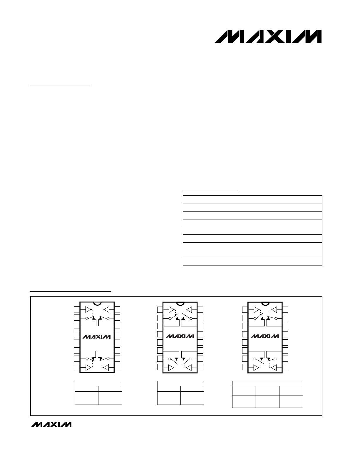
The MAX351/MAX352/MAX353 are precision, quad,
single-pole single-throw (SPST) analog switches. The
MAX351 has four normally closed (NC), and the MAX352
has four normally open (NO) switches. The MAX353 has
two NO and two NC switches. All three parts offer low on
resistance (less than 35Ω), guaranteed to match within 2Ω
between channels and to remain flat over the analog signal
range (∆3Ω max). They also offer low leakage (less than
250pA at +25°C and less than 6nA at +85°C) and fast
switching (turn-on time less than 175ns and turn-off time
less than 145ns).
The MAX351/MAX352/MAX353 are fabricated with Maxim’s
new improved 44V silicon-gate process. Design improvements guarantee extremely low charge injection (10pC), low
power consumption (35µW), and electrostatic discharge
(ESD) greater than 2000V. The 44V maximum breakdown
voltage allows rail-to-rail analog signal handling.
These monolithic switches operate with a single positive
supply (+10V to +30V) or with split supplies (±4.5V to ±20V)
while retaining CMOS-logic input compatibility and fast
switching. CMOS inputs provide reduced input loading.
________________________Applications
Sample-and-Hold Circuits Military Radios
Guidance and Control Systems Communications Systems
Heads-Up Displays Battery-Operated Systems
Test Equipment PBX, PABX
____________________________Features
♦ Low On Resistance < 22Ω Typical (35Ω Max)
♦ Guaranteed Matched On Resistance Between
Channels < 2Ω
♦ Guaranteed Flat On Resistance Over Analog
Signal Range ∆3Ω Max
♦ Guaranteed Charge Injection < 10pC
♦ Guaranteed Off-Channel Leakage < 6nA at +85°C
♦ ESD Guaranteed > 2000V per Method 3015.7
♦ Single-Supply Operation (+10V to +30V)
Bipolar-Supply Operation (±4.5V to ±20V)
♦ TTL-/CMOS-Logic Compatibility
♦ Rail-to-Rail Analog Signal Handling Capability
MAX351/MAX352/MAX353
Precision, Quad, SPST Analog Switches
________________________________________________________________ Maxim Integrated Products 1
Pin Configurations/Functional Diagrams/Truth Tables
19-0212; Rev 2; 9/01
Pin Configuration continued at end of data sheet.
Ordering Information continued at end of data sheet.
*Contact factory for availability and processing to MIL-STD-883.
Ordering Information
PART TEMP RANGE PIN-PACKAGE
MAX351CPE 0°C to +70°C 16 Plastic DIP
MAX351CSE 0°C to +70°C 16 Narrow SO
MAX351C/D 0°C to +70°C Dice*
MAX351EGE -40°C to +85°C 16 QFN
MAX351EPE -40°C to +85°C 16 Plastic DIP
MAX351ESE -40°C to +85°C 16 Narrow SO
MAX351EJE -40°C to +85°C 16 CERDIP
MAX351MJE -55°C to +125°C 16 CERDIP
TOP VIEW
COM1
NC1
GND
NC4
COM4
IN1
V-
IN4
1
2
3
4
5
6
7
8
MAX351
DIP/SO
MAX351
LOGIC SWITCH
0
1
IN1
COM1
NO1
V-
GND
NO4
COM4
IN4
1
2
3
4
5
6
7
8
LOGIC
0
1
MAX353
DIP/SO
MAX353
SWITCHES
1, 4
OFF
ON
16
IN2
15
COM2
14
NC2
13
V+
12
VL
11
NC3
10
COM3
9
IN3
SWITCHES
2, 3
ON
OFF
ON
OFF
16
15
14
13
12
11
10
9
IN2
COM2
NC2
V+
VL
NC3
COM3
IN3
1
IN1
2
COM1
3
NO1
V-
4
MAX352
5
GND
6
NO4
7
COM4
8
IN4
DIP/SO
MAX352
LOGIC SWITCH
0
1
SWITCHES SHOWN FOR LOGIC "0" INPUT
OFF
ON
16
15
14
13
12
11
10
9
IN2
COM2
NO2
V+
VL
NO3
COM3
IN3
Page 2
MAX351/MAX352/MAX353
Precision, Quad, SPST Analog Switches
2 _______________________________________________________________________________________
ABSOLUTE MAXIMUM RATINGS
Voltage Referenced to V-
V+.......................................................................................44V
GND ...................................................................................25V
VL ................................................(GND - 0.3V) to (V+ + 0.3V)
Digital Inputs, V
COM
, VNC, VNO(Note 1) ...........(V- - 2V) to (V+ + 2V)
.........................................................or 30mA (whichever occurs first)
Current (any terminal) .........................................................30mA
Peak Current COM_, NO_, NC_
(pulsed at 1ms, 10% duty cycle max) ..........................100mA
ESD per Method 3015.7 ..................................................>2000V
Continuous Power Dissipation (T
A
= +70°C) (Note 2)
Plastic DIP (derate 10.53mW/°C above +70°C) ..........842mW
Narrow SO (derate 8.70mW/°C above +70°C) ............696mW
QFN (derate 19.2mW/°C above +70°C) ....................1538mW
CERDIP (derate 10.00mW/°C above +70°C)...............800mW
Operating Temperature Ranges:
MAX35_C_ _ .......................................................0°C to +70°C
MAX35_E_ _.....................................................-40°C to +85°C
MAX35_MJE ..................................................-55°C to +125°C
Storage Temperature Range .............................-65°C to +150°C
Lead Temperature (soldering, 10s) .................................+300°C
ELECTRICAL CHARACTERISTICS—Dual Supplies
(V+ = 15V, V- = -15V, VL = 5V, GND = 0V, V
INH
= 2.4V, V
INL
= 0.8V, TA= T
MIN
to T
MAX
, unless otherwise noted.)
Stresses beyond those listed under “Absolute Maximum Ratings” may cause permanent damage to the device. These are stress ratings only, and functional
operation of the device at these or any other conditions beyond those indicated in the operational sections of the specifications is not implied. Exposure to
absolute maximum rating conditions for extended periods may affect device reliability.
Note 1: Signals on NC_, NO_, COM_, or IN_ exceeding V+ or V- will be clamped by internal diodes. Limit forward diode current to
maximum current rating.
Note 2: All leads are soldered or welded to PC board.
17 30
M
C, E
-40 40
-20 20
-20 20
-0.25 -0.10 0.25
5
4
M
M
M
TA= T
MIN
to T
MAX
TA= T
MIN
to T
MAX
C, E
C, E
C, E
TA= T
MIN
to T
MAX
TA=
+25°C
TA= T
MIN
to T
MAX
TA= +25°C
TA= T
MIN
to T
MAX
TA= +25°C
TA= T
MIN
to T
MAX
TA= +25°C
TA= +25°C
TA= +25°C
V
COM
= ±15.5V,
V
NO_
or V
NC_
= ±15.5V,
V+ = 16.5V,
V- = -16.5V
V
COM
= -15.5V,
V
NO_
or V
NC_
= 15.5V,
V+ = 16.5V,
V- = -16.5V
(Notes 1, 4)
V
COM
= -15.5V,
V
NO_
or V
NC_
= 15.5V,
V+ = 16.5V,
V- = -16.5V
I
COM
= -10mA,
V
NO_
or V
NC_
= ±10V,
V+ = 15V, V- = - 15V
I
COM
= -10mA,
V
NO_
or V
NC_
= ±8.5V,
V+ = 13.5V,
V- = -13.5V
I
COM
= -10mA,
V
NO_
or V
NC_
= ±5V,
V+ = 15V, V- = - 15V
CONDITIONS
nA
-10 10
I
COM(ON)
COM_ On Leakage Current
-0.4 -0.1 0.4
I
NC(OFF)
nA
-6 6
COM_ Off Leakage Current
-6 6
nA
I
NO
I
NC
Off Leakage Current
(NO_ or NC_)
-0.25 -0.10 0.25
Ω
3
R
ON
On Resistance Flatness (Note 5)
VV- V+
V
COM_
,
V
NO_
,
V
NC_
Analog Signal Range
R
ON
On Resistance Match Between
Channels (Note 5)
Ω
2
17 35
Ω
45
R
ON
On Resistance
UNITS
MIN TYP MAX
(Note 3)
SYMBOLPARAMETER
SWITCH
Page 3
MAX351/MAX352/MAX353
Precision, Quad, SPST Analog Switches
_______________________________________________________________________________________ 3
ELECTRICAL CHARACTERISTICS—Dual Supplies (continued)
(V+ = 15V, V- = -15V, VL = 5V, GND = 0V, V
INH
= 2.4V, V
INL
= 0.8V, TA= T
MIN
to T
MAX
, unless otherwise noted.)
ns
ns
-5 5TA= T
MIN
to T
MAX
-5 5TA= T
MIN
to T
MAX
TA= +25°C
-5 5TA= T
MIN
to T
MAX
-5 5TA= T
MIN
to T
MAX
TA= +25°C
TA= +25°C
TA= +25°C
TA= +25°C
TA= +25°C
TA= +25°C
TA= +25°C
TA= T
MIN
to T
MAX
TA= +25°C
TA= T
MIN
to T
MAX
TA= +25°C
TA= +25°C
TA= +25°C
CONDITIONS
TA= +25°C
-1 -0.0001 1
All channels on or off,
V
IN
= 0V or 5V,
V+ = 16.5V
V- = -16.5V
All channels on or off,
V
IN
= 0V or 5V,
V+ = 16.5V
V- = -16.5V
All channels on or off,
VIN= 0V or 5V,
V+ = 16.5V
V- = -16.5V
pF35f = 1MHz, Figure 8C
(COM)
On Capacitance
pF9f = 1MHz, Figure 7C
(COM)
COM Off Capacitance
pF9f = 1MHz, Figure 7C
(OFF)
NC or NO Capacitance
dB85
RL= 50Ω,
C
L
= 5pF,
f = 1MHz, Figure 6
Crosstalk (Note 7)
dB68
RL= 50Ω,
C
L
= 5pF,
f = 1MHz, Figure 5
OIRROff Isolation (Note 6)
pC510
CL= 1.0nF,
V
GEN
= 0V,
R
GEN
= 0Ω, Figure 4
QCharge Injection
ns25
MAX353 only, Figure 3,
RL= 300Ω,
C
L
= 35pF
t
D
Break-Before-Make Time Delay
Figure 2,
V
COM
= ±10V
Figure 2,
V
COM
= ±10V
160
t
OFF
Turn-Off Time
100 145
220
t
ON
Turn-On Time
µA-0.500 0.005 0.500I
INH
110 175
Input Current with Input Voltage
High
-1 -0.0001 1
µAI
GND
Ground Current
µA
-1 0.0001 1
I
L
Logic Supply Current
µA
-1 0.0001 1
I+Positive Supply Current
µA
µA
-0.500 0.005 0.500I
INL
Input Current with Input Voltage
Low
All channels on or off,
V
IN
= 0V or 5V,
V+ = 16.5V
V- = -16.5V
V
I-Negative Supply Current
±4.5 ±20.0Power-Supply Range
UNITS
MIN TYP MAX
(Note 3)
SYMBOLPARAMETER
IN_ = 2.4V, all others = 0.8V
IN_ = 0.8V, all others = 2.4V
INPUT
SUPPLY
DYNAMIC
Page 4
MAX351/MAX352/MAX353
Precision, Quad, SPST Analog Switches
4 _______________________________________________________________________________________
PARAMETER SYMBOL
MIN TYP MAX
(Note 3)
UNITS
Channel On Resistance R
ON
100
Ω
Logic Supply Current
Positive Supply Current I+
-1 0.0001 1
µA
I
L
-1 0.0001 1
µA
Negative Supply Current I-
-1 0.0001 1
µA
Ground Current
Analog Signal Range
I
GND
-1 -0.0001 1
µA
Turn-On Time
V
COM_,
V
NO_,
V
NC
0V+V
175 250
nst
ON
95 125
40 80
Turn-Off Time t
OFF
140
ns
I
COM
= -10mA,
V
NC_
or V
NO_
= 3.8V,
V+ = 10.8V
V+ = 13.2V,
all channels on or off,
V
IN
= 0V or 5V
VL = 5.25V,
all channels on or off,
V
IN
= 0V or 5V
V+ = 13.2V,
all channels on or off,
V
IN
= 0V or 5V
VL = 5.25V,
all channels on or off,
V
IN
= 0V or 5V
Figure 2,
V
NO_
or V
NC_
= 8V
Figure 2,
V
NO_
or V
NC_
= 8V
ELECTRICAL CHARACTERISTICS—Single Supply
(V+ = 12V, V- = 0V, VL = 5V, GND = 0V, V
INH
= 2.4V, V
INL
= 0.8V, TA= T
MIN
to T
MAX
, unless otherwise noted.)
Break-Before-Make Time Delay
t
D
MAX353 only, Figure 3,
R
L
= 300Ω,
CL= 35pF
25 ns
Charge Injection Q
Figure 8,
C
L
= 1.0nF,
V
GEN
= 0V,
R
GEN
= 0V
510pC
CONDITIONS
TA= T
MIN
to T
MAX
TA= +25°C
TA= +25°C
TA= +25°C
(Notes 1, 4)
TA= +25°C
TA= +25°C
TA= +25°C
TA= T
MIN
to T
MAX
TA= +25°C
TA= +25°C
TA= T
MAX
-5 5
TA= T
MIN
to T
MAX
315
TA= T
MAX
-5 5
TA= T
MAX
-5 5
TA= T
MAX
TA= +25°C
-5 5
Note 3: The algebraic convention, where the most negative value is a minimum and the most positive value a maximum, is used in
this data sheet.
Note 4: Guaranteed by design.
Note 5: ∆R
ON
= ∆RONmax - ∆RONmin. On-resistance match between channels and flatness are guaranteed only with
bipolar-supply operation.
Note 6: See Figure 5. Off Isolation = 20 log
10
[ V
COM
⁄ (V
NC or VNO
)
], V
COM
= output, V
NC or VNO
= input to off switch.
Note 7: Between any two switches. See Figure 6.
DYNAMIC
SUPPLY
SWITCH
Page 5

MAX351/MAX352/MAX353
Precision, Quad, SPST Analog Switches
_______________________________________________________________________________________ 5
__________________________________________Typical Operating Characteristics
(TA = +25°C, unless otherwise noted.)
ON RESISTANCE vs. V
POWER-SUPPLY VOLTAGE
70
A: V+ = 5V,
V- = -5V
60
B: V+ = 10V,
V- = -10V
50
C: V+ = 15V,
V- = -15V
40
D: V+ = 20V,
(Ω)
ON
R
V- = -20V
30
20
10
0
-20 -10 10
ON RESISTANCE vs. V
(SINGLE-SUPPLY)
80
V+ = 12V
V- = 0V
70
60
(Ω)
50
ON
R
40
30
020
V
(V)
COM
AND
COM
A
B
COM
TA = +125°C
TA = +85°C
TA = +25°C
ON RESISTANCE vs. V
TEMPERATURE
60
MAX351-01
C
D
V+ = 15V
V- = -15V
50
40
(Ω)
30
ON
R
20
10
0
-20 -10 10
TA = +125°C
TA = +25°C
TA = -55°C
OFF LEAKAGE CURRENTS vs.
TA = +85°C
020
V
(V)
COM
TEMPERATURE
100
MAX351-04
V+ = 16.5V
V- = -16.5V
10
V
COM
OR VNO = +15V
V
NC
1
0.1
0.01
OFF LEAKAGE (nA)
0.001
= ±15V
COM
AND
160
MAX351-02
140
120
100
(Ω)
ON
R
80
60
40
20
100
MAX351-05
10
1
0.1
0.01
ON LEAKAGE (nA)
0.001
ON RESISTANCE vs. V
COM
AND
TEMPERATURE
V- = 0V
V+ = 5V
V+ = 10V
V+ = 15V
05 15
10 20
V
(V)
COM
V+ = 20V
ON LEAKAGE CURRENTS vs.
TEMPERATURE
V+ = 16.5V
V- = -16.5V
= ±15V
V
COM
OR VNO = ±15V
V
NC
MAX351-03
MAX351-06
20
05 15
10 20
V
(V)
COM
60
40
20
0
Q (pC)
-20
-40
-60
-20
0.0001
-55
CHARGE INJECTION vs.
ANALOG VOLTAGE
V+ = 15V
V- = -15V
VL = 5V
-15 -10 -5 5 10 15
CL = 1nF
020
V
(V)
COM
+25 +125
TEMPERATURE (°C)
MAX351-07
V
NC
(µA)
L
I+, I-, I
0.001
0.0001
0.0001
SUPPLY CURRENT vs. TEMPERATURE
100
A: I+ at V+ = 16.5V
B: I- at V- = -16.5V
10
1
0.1
0.01
-55
C: I
A
B
C
at VL = 5V
L
+25 +125
TEMPERATURE (°C)
-55
+25 +125
TEMPERATURE (°C)
MAX351-08
Page 6

MAX351/MAX352/MAX353
__________Applications Information
Operation with Supplies Other than ±15V
The main limitation of supply voltages other than
±15V is reduced analog-signal range. The MAX351/
MAX352/MAX353 operate with ±5V to ±20V bipolar
supplies. The Typical Operating Characteristics graphs
show typical on resistance (RON) for ±15V, ±10V, and
±5V supplies. (Switching times increase by a factor of
two or more for operation at ±5V.) The MAX351/
MAX352/MAX353 can operate from +10V to +30V
unipolar supplies. Each device can also be powered
from unbalanced supplies such as +24V and -5V.
Connect V- to 0V when operating with a single supply.
VL must be connected to +5V to be TTL compatible or
to V+ for CMOS-logic input levels.
Overvoltage Protection
Proper power-supply sequencing is recommended for
all CMOS devices. Do not exceed the absolute maximum ratings because stresses beyond the listed ratings may cause permanent damage to the devices.
Always sequence V+ first, followed by VL, V-, and logic
inputs. If power-supply sequencing is not possible, add
two small signal diodes in series with the supply pins
for overvoltage protection (Figure 1). Adding diodes
reduces the analog signal range to 1V below V+ and
1V below V-, but low switch resistance and low-leakage
characteristics are unaffected. Device operation is
unchanged, and the difference between V+ to Vshould not exceed +44V.
Precision, Quad, SPST Analog Switches
6 _______________________________________________________________________________________
______________________________________________________________Pin Description
Figure 1. Overvoltage Protection Using External Blocking
Diodes
PIN
DIP/SO QFN
NAME FUNCTION
IN1–N4 Logic Control Input
Analog Switch Common Terminal
NO or NC Analog Switch NO or NC Terminal
4 2 V- Negative-Supply Voltage Input
5 3 GN D Ground
12 10 V
L
Logic Supply Voltage
13 11 V+ Positive-Supply Voltage Input—Connected To Substrate
1, 16, 9, 8 15, 14, 7, 6
2, 15, 10, 7 16, 13, 8, 5 COM1–COM4
3, 15, 11, 6 1, 12, 9, 4
V+
V+
NO_
V
g
V-
COM_
V-
Page 7

MAX351/MAX352/MAX353
Precision, Quad, SPST Analog Switches
_______________________________________________________________________________________ 7
Figure 2. Switching-Time Test Circuit
Figure 3. Break-Before-Make Test Circuit (MAX353 only)
______________________________________________Test Circuits/Timing Diagrams
+3V
LOGIC
INPUT
SWITCH
OUTPUT
0V
0V
50%
V
O
0.9V
t
ON
LOGIC INPUT WAVEFORMS INVERTED FOR SWITCHES
THAT HAVE THE OPPOSITE LOGIC SENSE.
LOGIC
INPUT
SWITCH
OUTPUT 1
(VO1)
SWITCH
OUTPUT 2
(VO2)
+3V
50%
0V
0V
0V
t
D
0.9V
tr < 20ns
tf < 20ns
SWITCH
V
COM1
INPUT
t
OFF
0
01
0.9V
0
0.9V
02
t
D
V
V
COM1
COM2
LOGIC
INPUT
LOGIC
INPUT
= +10V
= +10V
C
INCLUDES FIXTURE AND STRAY CAPACITANCE.
L
+5V
VL
COM1
IN1
GND
0V
REPEAT TEST FOR IN AND S, FOR LOAD
CONDITIONS, SEE Electrical Characteristics
C
INCLUDES FIXTURE AND STRAY CAPACITANCE.
L
V
= V
O
COM (
RL + RON
+5V
VL
COM_
COM_
IN_
GND
RL
+15V
V+
V-
-15V
+15V
OR NC1
)
NO_
NC_
V+
V-
-15V
NO1
SWITCH
OUTPUT
V
O
R
300Ω
R
L2
RL = 300Ω
C
L
V
O2
C
L
L2
= 35pF
C
35pF
R
L
V
O1
C
L1
L1
Page 8

MAX351/MAX352/MAX353
Precision, Quad, SPST Analog Switches
8 _______________________________________________________________________________________
Figure 6. Crosstalk Test Circuit
Figure 5. Off-Isolation Test Circuit
Figure 4. Charge-Injection Test Circuit
_________________________________Test Circuits/Timing Diagrams (continued)
+5V
VL
R
GEN
COM
V
GEN
GND
+15V
V+
NC OR
NO
V-
IN
-15V
= +3V
V
IN
V
O
C
L
+15V
C
SIGNAL
GENERATOR 0dBm
ANALYZER
COM
R
L
V+
COM
NC OR NO
GND
+5V
VL
0V,
IN
V-
2.4V
C
V
O
IN
OFF
OFF
IN
SIGNAL
GENERATOR 0dBm
0V, 2.4V
ANALYZER
∆V
O
+5V
VL
OFF
OFF
N01
IN2
COM2
V-
ON
ON
Q = (∆VO)(CL)
IN DEPENDS ON SWITCH CONFIGURATION;
INPUT POLARITY DETERMINED BY SENSE OF SWITCH.
C
+15V
V+
COM1
IN1
N02
R
L
GND
50Ω
0V, 2.4V
NC
C
-15V
-15V
Page 9

MAX351/MAX352/MAX353
Precision, Quad, SPST Analog Switches
_______________________________________________________________________________________ 9
_________________________________Test Circuits/Timing Diagrams (continued)
Pin Configurations (continued)
Figure 7. Channel-Off Capacitance
Figure 8. Channel-On Capacitance Test Circuit
CAPACITANCE
METER
f = 1MHz
+15V
C
V+
COM
NC OR NO
GND
+5V
V-
-15V
VL
CAPACITANCE
IN
2.4V
C
METER
f = 1MHz
+15V
C
V+
COM
NC OR NO
GND
+5V
V-
-15V
VL
IN
0V
C
TOP VIEW
COM1
16
1NC1
IN1
IN2
COM2
15
14
13
12 NC2
NO1
COM1
IN1
16 15 14 13
1
IN2
COM2
NO2
12
NC4
2V-
3GND
4
COM4
MAX351
5
6
7
IN4
IN3
NO1
V-
GND
NO4
11 V+
10 V
9
NC3
8
COM3
COM1
IN1
16 15 14 13
1
2
3
4
5
IN4
COM4
L
MAX353
6
V-
GND
NO4
IN2
IN3
2
3
4
COM2
7 8
COM3
5
COM4
11
V+
MAX352
6
IN4
7 8
IN3
COM3
V
10
L
9
NO3
QFN
NC2
12
11
V+
V
10
L
9
NC3
Page 10

MAX351/MAX352/MAX353
Precision, Quad, SPST Analog Switches
10 ______________________________________________________________________________________
___________________Chip Topography
TRANSISTOR COUNT: 136
SUBSTRATE CONNECTED TO V+
*Contact factory for availability and processing to MIL-STD-883.
Ordering Information (continued)
PART TEMP RANGE PIN-PACKAGE
MAX352CPE 0°C to +70°C 16 Plastic DIP
MAX352CSE 0°C to +70°C 16 Narrow SO
MAX352C/D 0°C to +70°C Dice*
MAX352EGE -40°C to +85°C 16 QFN
MAX352EPE -40°C to +85°C 16 Plastic DIP
MAX352ESE -40°C to +85°C 16 Narrow SO
MAX352EJE -40°C to +85°C 16 CERDIP
MAX352MJE -55°C to +125°C 16 CERDIP
MAX353CPE 0°C to +70°C 16 Plastic DIP
MAX353CSE 0°C to +70°C 16 Narrow SO
MAX353C/D 0°C to +70°C Dice*
MAX353EGE -40°C to +85°C 16 QFN
MAX353EPE -40°C to +85°C 16 Plastic DIP
MAX353ESE -40°C to +85°C 16 Narrow SO
MAX353EJE -40°C to +85°C 16 CERDIP
MAX353MJE -55°C to +125°C 16 CERDIP
COM1 IN1 IN2
A
V-
GND
B
COM4
IN4
0.080"
(2.03mm)
IN3
COM2
C
0.097"
(2.46mm)
V+
VL
D
COM3
MAX351 MAX352 MAX353
PIN NAME
A
B
C
D
NC
NC
NC
NC
A
B
C
D
NAME NAMEPIN PIN
NO
NO
NO
NO
A
B
C
D
NO
NO
NC
NC
Page 11

MAX351/MAX352/MAX353
Precision, Quad, SPST Analog Switches
______________________________________________________________________________________ 11
Package Information
(The package drawing(s) in this data sheet may not reflect the most current specifications. For the latest package outline information,
go to www.maxim-ic.com/packages.)
D1
E
D
E1
A3
A2
A
L
A1
e
B
B1
α
C
e
A
e
B
DIM
A1
A2
A3
B1
D1
E1
e
e
INCHES MILLIMETERS
MAX
MIN
A
0.015
0.125
0.055
B
0.016
0.050
C
0.008
D
0.745
0.005
E
0.300
0.240
e
A
B
L
0.115
α
0.200
–
0.150
0.080
0.022
0.065
0.012
0.765
0.030
0.325
0.280
0.100 BSC
0.300 BSC
0.400
–
0.150
0˚
–
15˚
16-PIN PLASTIC
DUAL-IN-LINE
PACKAGE
MIN
–
0.38
3.18
1.40
0.41
1.27
0.20
18.92
0.13
7.62
6.10
2.54 BSC
7.62 BSC
–
2.92
0˚
MAX
5.08
–
3.81
2.03
0.56
1.65
0.30
19.43
0.76
8.26
7.11
10.16
3.81
15˚
21-587A
DIM
A1
HE
D
h x 45˚
α
INCHES MILLIMETERS
MAX
MIN
A
0.053
0.004
B
0.014
C
0.007
D
0.386
E
0.150
e
H
0.228
h
0.010
L
0.016
α
0.069
0.010
0.019
0.010
0.394
0.157
0.244
0.020
0.050
0˚
8˚
MIN
1.35
0.10
0.35
0.19
9.80
3.80
5.80
0.25
0.40
0˚
MAX
1.75
0.25
0.49
0.25
10.00
4.00
1.27 BSC0.050 BSC
6.20
0.50
1.27
8˚
21-588B
A
0.127mm
e
B
A1
0.004in.
C
L
16-PIN PLASTIC
SMALL-OUTLINE
(NARROW)
PACKAGE
Page 12

MAX351/MAX352/MAX353
Precision, Quad, SPST Analog Switches
12 ______________________________________________________________________________________
Package Information (continued)
(The package drawing(s) in this data sheet may not reflect the most current specifications. For the latest package outline information,
go to www.maxim-ic.com/packages.)
S1
A
D
Q
L
e
B1
S
α
L1
B
E1
DIM
A
B
B1
C
D
E
E1
e
L
L1
E
Q
S
S1
α
C
INCHES MILLIMETERS
MIN
0.014
0.038
0.008
0.220
0.290
0.125
0.150
0.015
0.005
MAX
0.200
–
0.023
0.065
0.015
0.840
–
0.310
0.320
0.200
0.060
0.080
–
0˚
15˚
MIN
–
0.36
0.97
0.20
–
5.59
7.37
2.54 BSC0.100 BSC
3.18
–
3.81
0.38
–
–
0.13
0˚
16-PIN CERAMIC
MAX
5.08
0.58
1.65
0.38
21.34
7.87
8.13
5.08
–
1.52
2.03
–
15˚
21-590B
DUAL-IN-LINE
PACKAGE
Page 13

MAX351/MAX352/MAX353
Precision, Quad, SPST Analog Switches
Maxim cannot assume responsibility for use of any circuitry other than circuitry entirely embodied in a Maxim product. No circuit patent licenses are
implied. Maxim reserves the right to change the circuitry and specifications without notice at any time.
Maxim Integrated Products, 120 San Gabriel Drive, Sunnyvale, CA 94086 408-737-7600 ____________________ 13
© 2001 Maxim Integrated Products Printed USA is a registered trademark of Maxim Integrated Products.
Package Information (continued)
(The package drawing(s) in this data sheet may not reflect the most current specifications. For the latest package outline information,
go to www.maxim-ic.com/packages.)
32L QFN .EPS
 Loading...