General Description
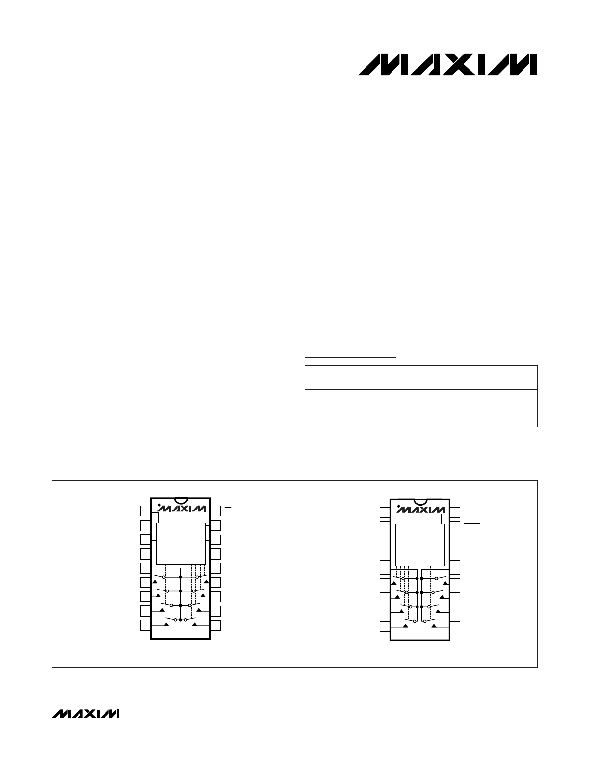
The MAX349/MAX350 are 8-channel and dual 4-channel
serially controlled multiplexers (muxes). These muxes
conduct equally well in either direction. On-resistance
(100Ω max) is matched between switches to 16Ω max
and is flat (10Ω max) over the specified signal range.
These CMOS devices can operate continuously with
dual power supplies ranging from ±2.7V to ±8V or a single supply between +2.7V and +16V. Each mux can
handle rail-to-rail analog signals. The off-leakage current
is only 0.1nA at +25°C or 5nA at +85°C.
Upon power-up, all switches are off and the internal
shift registers are reset to zero.
The serial interface is compatible with SPI™/QSPI™
and MICROWIRE™. Functioning as a shift register, it
allows data (at DIN) to be clocked in synchronously
with the rising edge of clock (SCLK). The shift register’s
output (DOUT) enables several MAX349s or MAX350s
to be daisy chained.
All digital inputs have 0.8V or 2.4V logic thresholds,
ensuring both TTL and CMOS-logic compatibility when
using ±5V supplies or a single +5V supply.
________________________Applications
Serial Data-Acquisition Industrial and ProcessSystems Control Systems
Avionics ATE Equipment
Audio Signal Routing Networking
____________________________Features
♦ SPI/QSPI, MICROWIRE-Compatible Serial
Interface
♦ 8 Separately Controlled SPST Switches
♦ Single 8-to-1 Mux (MAX349)
Dual 4-to-1 Mux (MAX350)
♦ 100Ω Signal Paths with ±5V Supplies
♦ Rail-to-Rail
®
Signal Handling
♦ Asynchronous RESET Input
♦ ±2.7V to ±8V Dual Supplies
+2.7V to +16V Single Supply
♦ >2kV ESD Protection per Method 3015.7
♦ TTL/CMOS-Compatible Inputs (with +5V or ±5V
Supplies)
MAX349/MAX350
Serially Controlled, Low-Voltage,
8-Channel/Dual 4-Channel Multiplexers
________________________________________________________________
Maxim Integrated Products
1
18
17
16
15
14
13
12
11
1
2
3
4
5
6
7
8
CS
RESET
DOUT
V-
GND
DIN
V+
SCLK
TOP VIEW
N.C.
NO7
NO6
NO5
NO2
NO1
NO0
COM
10
9
NO4
NO3
DIP/SO
MAX349
LOGIC
18
17
16
15
14
13
12
11
1
2
3
4
5
6
7
8
CS
RESET
DOUT
V-
GND
DIN
V+
SCLK
COMB
NO0B
NO1B
NO2B
NO2A
NO1A
NO0A
COMA
10
9
NO3B
NO3A
DIP/SO
MAX350
LOGIC
N.C. = NOT INTERNALLY
CONNECTED
Pin Configurations/Functional Diagrams
19-0451; Rev 1; 10/98
PART
MAX349CPN
MAX349CWN
MAX349CAP 0°C to +70°C
0°C to +70°C
0°C to +70°C
TEMP. RANGE PIN-PACKAGE
18 Plastic DIP
18 Wide SO
20 SSOP
Ordering Information
Ordering Information continued at end of data sheet.
*Contact factory for dice specifications.
MAX349C/D 0°C to +70°C Dice*
Pin Configurations continued at end of data sheet.
SPI and QSPI are trademarks of Motorola, Inc. MICROWIRE is a trademark of National Semiconductor Corp.
Rail-to-Rail is a registered trademark of Nippon Motorola, Ltd.
For free samples & the latest literature: http://www.maxim-ic.com, or phone 1-800-998-8800.
For small orders, phone 1-800-835-8769.
MAX349/MAX350
Serially Controlled, Low-Voltage,
8-Channel/Dual 4-Channel Multiplexers
2 _______________________________________________________________________________________
ABSOLUTE MAXIMUM RATINGS
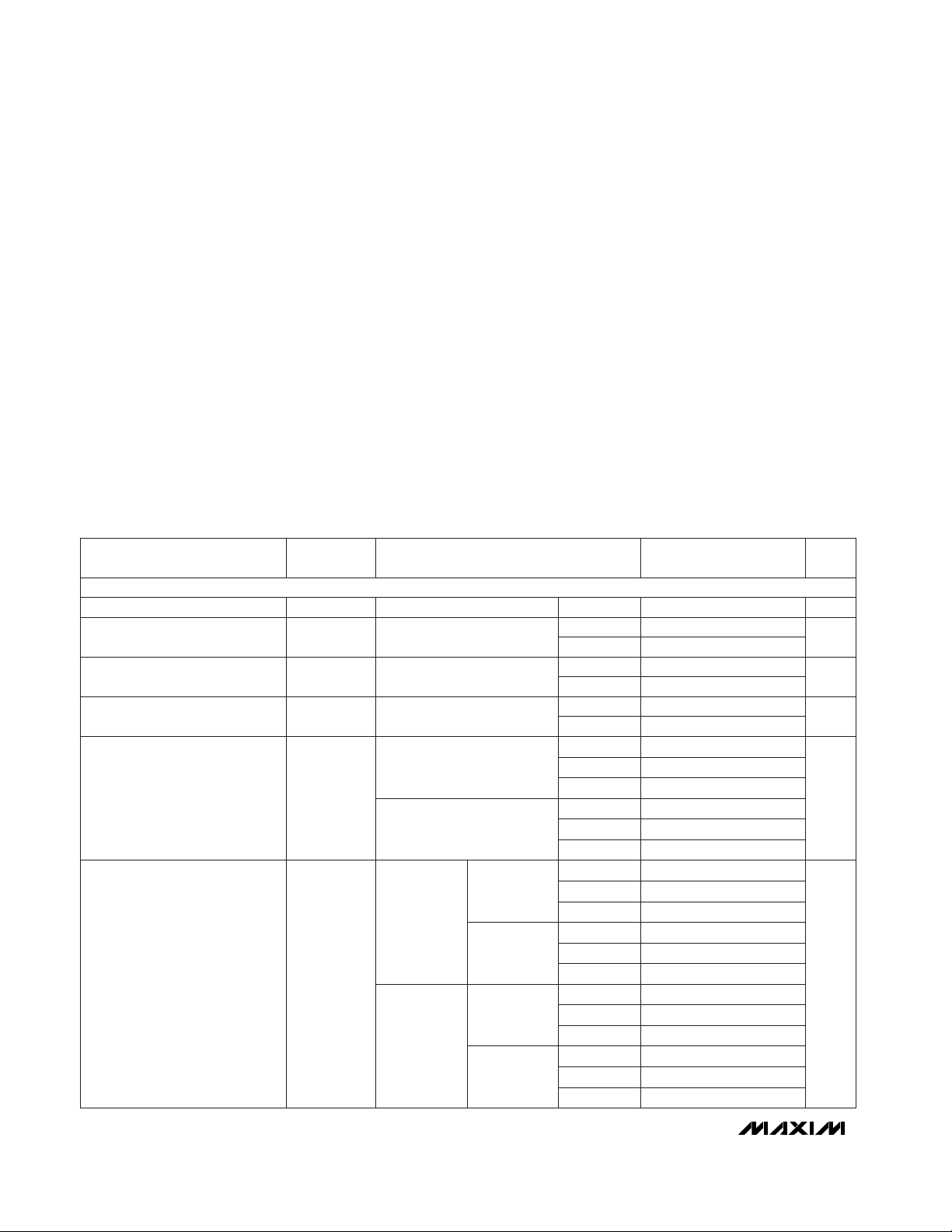
ELECTRICAL CHARACTERISTICS—Dual Supplies
(V+ = +4.5V to +5.5V, V- = -4.5V to -5.5V, TA= T
MIN
to T
MAX
, unless otherwise noted. Typical values are at TA= +25°C.)
Stresses beyond those listed under “Absolute Maximum Ratings” may cause permanent damage to the device. These are stress ratings only, and functional
operation of the device at these or any other conditions beyond those indicated in the operational sections of the specifications is not implied. Exposure to
absolute maximum rating conditions for extended periods may affect device reliability.
Voltages Referenced to GND
V+...........................................................................-0.3V, +17V
V-............................................................................-17V, +0.3V
V+ to V-...................................................................-0.3V, +17V
SCLK,
CS, DIN, DOUT, RESET .................-0.3V to (V+ + 0.3V)
NO, COM.................................................(V- - 2V) to (V+ + 2V)
Continuous Current into Any Terminal..............................±30mA
Peak Current, NO or COM
(pulsed at 1ms, 10% duty cycle).................................±100mA
Continuous Power Dissipation (T
A
= +70°C)
18-Pin Plastic DIP (derate 11.11mW/°C above +70°C) ..889mW
18-Pin SO (derate 9.52mW/°C above +70°C)...............762mW
20-Pin SSOP (derate 8.00mW/°C above +70°C) ..........640mW
18-Pin CERDIP (derate 10.53mW/°C above +70°C).....842mW
Operating Temperature Ranges
MAX349C_ _, MAX350C_ _ .................................0°C to +70°C
MAX349E_ _, MAX350E_ _...............................-40°C to +85°C
MAX349M_ _, MAX350M_ _ ...........................-55°C to +125°C
Storage Temperature Range.............................-65°C to +150°C
Lead Temperature (soldering, 10sec).............................+300°C
CONDITIONS UNITS
MIN TYP MAX
(Note 1)
SYMBOLPARAMETER
60 100
VV- V+V
COM
, V
NO
Analog Signal Range
V+ = 5V, V- = -5V,
V
COM
= ±3V, INO= 1mA
Ω
125
R
ON
COM-NO On-Resistance
C, E, M
TA= +25°C
C, E, M
TA= +25°C 16
C, E, M
V+ = 5V, V- = -5V,
V
COM
= ±3V, INO= 1mA
Ω
20
∆R
ON
COM-NO On-Resistance Match
Between Channels (Note 2)
TA= +25°C 10
C, E, M
V+ = 5V, V- = -5V, INO= 1mA,
V
COM
= -3V, 0V, 3V
Ω
15
R
FLAT(ON)
COM-NO On-Resistance
Flatness (Note 2)
TA= +25°C -0.1 0.002 0.1
ANALOG SWITCH
C, E -5 5
V+ = 5.5V, V- = -5.5V,
V
COM
= -4.5V, VNO= 4.5V
M -10 10
TA= +25°C -0.1 0.002 0.1
C, E -5 5
NO Off-Leakage Current
(Note 3)
I
NO(OFF)
V+ = 5.5V, V- = -5.5V,
V
COM
= 4.5V, VNO= -4.5V
M -10 10
nA
TA= +25°C -0.1 0.002 0.1
C, E -10 10
M -100 100
TA= +25°C -0.1 0.002 0.1
C, E -5 5
V+ = 5.5V,
V- = -5.5V,
V
COM
=
±4.5V,
VNO= ±4.5V
M -50 50
TA= +25°C -0.2 0.002 0.2
C, E -10 10
M -100 100
TA= +25°C -0.2 0.002 0.2
C, E -5 5
COM Off-Leakage Current
(Note 3)
I
COM(OFF)
V+ = 5.5V,
V- = -5.5V,
V
COM
=
-4.5V,
VNO= 4.5V
M -50 50
nA
MAX349
MAX349
MAX350
MAX350
MAX349/MAX350
Serially Controlled, Low-Voltage,
8-Channel/Dual 4-Channel Multiplexers
_______________________________________________________________________________________ 3
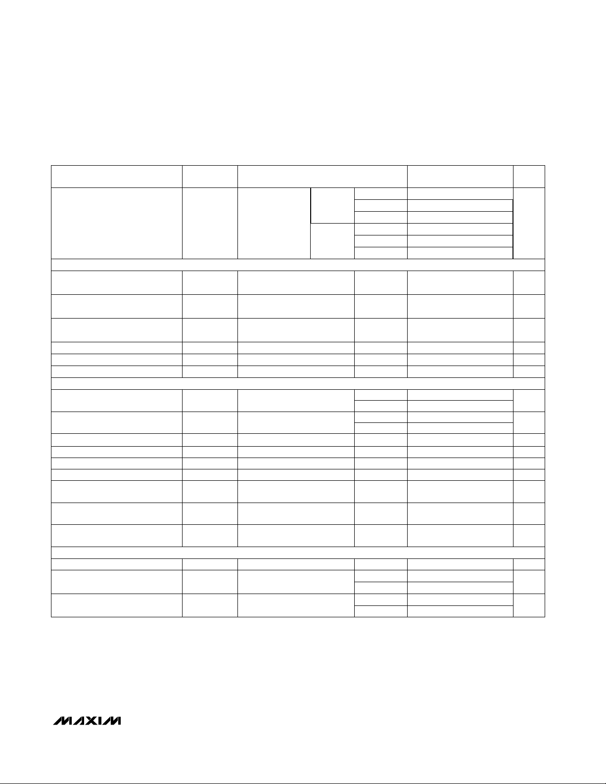
ELECTRICAL CHARACTERISTICS—Dual Supplies (continued)
(V+ = +4.5V to +5.5V, V- = -4.5V to -5.5V, TA= T
MIN
to T
MAX
, unless otherwise noted. Typical values are at TA= +25°C.)
V2.4C, E, MV
IH
DIN, SCLK, CS, RESET Input
Voltage Logic Threshold High
MAX350
nA
-50 50M
V+ = 5.5V,
V- = -5.5V,
V
COM
= V
NO
=
±4.5V
COM On-Leakage Current
(Note 3)
I
COM(ON)
-5 5C, E
MAX349
-0.2 0.02 0.2TA= +25°C
-100 100M
-10 10C, E
DOUT Output Voltage Logic Low V
DOUT
VI
DOUT
= -1.6mA 0 0.4C, E, M
mV100C, E, M
DOUT Output Voltage Logic High V
DOUT
SCLK
HYST
VI
DOUT
= 0.8mA
SCLK Input Hysteresis
2.8 V+C, E, M
µA-1 0.03 1C, E, M
V
DIN
, V
SCLK
,
VCS= 0.8V or 2.4V
I
IH, IIL
DIN, SCLK, CS, RESET Input
Current Logic High or Low
V0.8C, E, MV
IL
DIN, SCLK, CS, RESET Input
Voltage Logic Threshold Low
-0.2 0.001 0.2TA= +25°C
Turn-On Time t
ON
400
ns
From rising edge of CS
C, E, M
200 275TA= +25°C
-2 2
30
C, E, M
C, E, M
RL= 50Ω, CL= 15pF,
V
NO
= 1V
RMS
, f = 100kHz
Off-Isolation V
ISO
dB
pC
pF
pF
Charge Injection (Note 4)
NO Off-Capacitance
COM Off-Capacitance
V
CTE
C
NO(OFF)
C
COM(OFF)VCOM
= GND, f = 1MHz
CL= 1nF, VNO= 0V, RS= 0Ω
Break-Before-Make Delay t
BBM
2
ns
VNO= GND, f = 1MHz
TA= +25°C
2TA= +25°C
110
From rising edge of CS
TA= +25°C
540TA= +25°C
PARAMETER SYMBOL
MIN TYP MAX
(Note 1)
UNITS
V+ Supply Current I+
720
µA
V- Supply Current I-
-1 0.1 1
µA
Turn-Off Time t
OFF
300
ns
From rising edge of CS
C, E, M
90 150TA= +25°C
DIN = CS = SCLK = 0V or V+,
RESET = 0V or V+
DIN = CS = SCLK = 0V or V+,
RESET = 0V or V+
Channel-to-Channel Crosstalk V
CT
dB< -90
RL= 50Ω, CL= 15pF,
VNO= 1V
RMS
, f = 100kHz
TA= +25°C
Switch On-Capacitance C
(ON)
> 90
C, E, M
TA= +25°C
pF
Power-Supply Range V+, V- ±3 ±8 V
TA= +25°C
8
CONDITIONS
V
COM
= VNO= GND,
f = 1MHz
TA= +25°C
TA= +25°C
DIGITAL I/O
SWITCH DYNAMIC CHARACTERISTICS
POWER SUPPLY
MAX349/MAX350
Serially Controlled, Low-Voltage,
8-Channel/Dual 4-Channel Multiplexers
4 _______________________________________________________________________________________
SCLK Frequency f
SCLK
RESET Minimum Pulse Width
t
RW
70 nsTA= +25°C
Fall Time of DOUT (Note 4) t
DF
100 ns
20% of V+ to 70% of V+,
CL= 10pF
C, E, M
Allowable Fall Time at DIN, SCLK
(Note 4)
t
SCF
2 µs
20% of V+ to 70% of V+,
CL= 10pF
C, E, M
Allowable Rise Time at DIN, SCLK
(Note 4)
t
SCR
2 µs
20% of V+ to 70% of V+,
CL= 10pF
C, E, M
Rise Time of DOUT (Note 4) t
DR
100 ns
20% of V+ to 70% of V+,
CL= 10pF
C, E, M
DIN Data Valid after Falling SCLK
(Note 4)
t
DO
400
ns
Data Hold Time
Minimum Data Setup Time t
DS
17 100 ns
t
DH
0 -17
85
50% of SCLK to 10% of DOUT,
CL= 10pF
SCLK Low Time
ns
t
CL
C, E, M
190 ns
TA= +25°C
C, E, M
C, E, M
PARAMETER SYMBOL
MIN TYP MAX
(Note 1)
UNITS
C, E, M
SCLK High Time
CS Lag Time
t
CSH2
240 ns
t
CH
190
CS Lead Time
Cycle Time
ns
t
CH +tCL
480
t
CSS
240 ns
C, E, M
0 2.1nsMHz
C, E, M
C, E, M
C, E, M
C, E, M
CONDITIONS
SERIAL DIGITAL INTERFACE
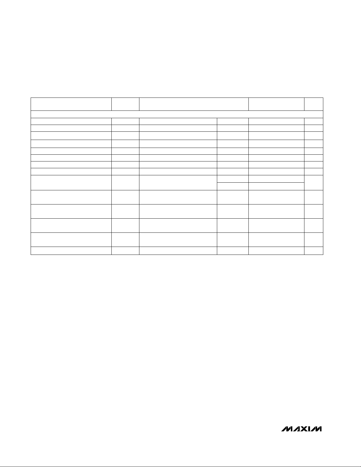
TIMING CHARACTERISTICS—Dual Supplies (Figure 1)
(V+ = +4.5V to +5.5V, V- = -4.5V to -5.5V, TA= T
MIN
to T
MAX
, unless otherwise noted. Typical values are at TA= +25°C.)
Note 1: The algebraic convention is used in this data sheet; the most negative value is shown in the minimum column.
Note 2: ∆R
ON
= R
ON(max)
- R
ON(min)
. On-resistance match between channels and on-resistance flatness are guaranteed only with
specified voltages. Flatness is defined as the difference between the maximum and minimum value of on-resistance as
measured over the specified analog signal range.
Note 3: Leakage parameters are 100% tested at maximum rated hot temperature and guaranteed by correlation at room temp.
Note 4: Guaranteed by design.
Note 5: Leakage testing at single supply is guaranteed by testing with dual supplies.
Note 6: See Figure 6. Off-isolation = 20log
10VCOM/VNO
, V
COM
= output. NO = input to off switch.
Note 7: Between any two switches. See Figure 3.
MAX349/MAX350
Serially Controlled, Low-Voltage,
8-Channel/Dual 4-Channel Multiplexers
_______________________________________________________________________________________ 5
ELECTRICAL CHARACTERISTICS—Single +5V Supply
(V+ = +4.5V to +5.5V, V- = 0V, TA= T
MIN
to T
MAX
, unless otherwise noted. Typical values are at TA= +25°C.)
TA= +25°C
C, E, M
125 175
C, E, M
VV- V+V
COM
, V
NO
Analog Signal Range
TA= +25°C -0.1 0.002 0.1
TA= +25°C -0.2 0.002 0.2
C, E
C, E
CONDITIONS
-10 10
-10 10
V+ = 5V, V
COM
= 3.5V,
INO= 1mA
M -100 100
TA= +25°C
M -100 100
TA= +25°C -0.2 0.002 0.2
MAX349
C, E -5 5
M
Ω
225
R
ON
COM-NO On-Resistance
-50 50
-0.1 0.002 0.1
nA
V+ = 5.5V,
V
COM
= 0V,
VNO= 4.5V
MAX350
I
COM(OFF)
COM Off-Leakage Current
(Notes 4, 5)
TA= +25°C -0.2 0.01 0.2
C, E -10 10
M -100 100
TA= +25°C -0.2 0.02 0.2
MAX349
C, E -5 5
M
MAX349
-50 50
C, E -5 5
M -50 50
V+ = 5.5V,
V
COM
= VNO=
±4.5V
nA
MAX350
V+ = 5.5V,
V
COM
= 4.5V,
VNO= 0V
I
COM(ON)
COM On-Leakage Current
(Notes 4, 5)
MAX350
UNITS
MIN TYP MAX
(Note 1)
SYMBOLPARAMETER
TA= +25°C -0.1 0.002 0.1
C, E -5 5
M
V+ = 5.5V, V
COM
= 4.5V,
VNO= 0V
-10 10
C, E, M 2.4
C, E, M 0.8V
IL
V
IH
DIN, SCLK, CS, RESET Input
Voltage Logic Threshold Low
DIN, SCLK, CS, RESET Input
Voltage Logic Threshold High
V
V
C, E, M -1 0.03 1
C, E, M 2.8 V+
C, E, M 0 0.4I
DOUT
= -1.6mA
I
DOUT
= 0.8mA
V
DIN
, V
SCLK
,
VCS= 0.8V or 2.4V
V
DOUT
V
DOUT
IIH, I
IL
DOUT Output Voltage Logic Low
DOUT Output Voltage Logic High
DIN, SCLK, CS, RESET Input
Current Logic High or Low
V
V
µA
C, E, M 100SCLK
HYST
SCLK Input Hysteresis mV
TA= +25°C 720
C, E, M 30
DIN = CS = SCLK = 0V or V+,
RESET = 0V or V+
I+V+ Supply Current µA
TA= +25°C -0.1 0.002 0.1
C, E -5 5
M
V+ = 5.5V, V
COM
= 0V,
VNO= 4.5V
nA
-10 10
I
NO(OFF)
NO Off-Leakage Current
(Notes 4, 5)
DIGITAL I/O
ANALOG SWITCH
POWER SUPPLY
MAX349/MAX350
Serially Controlled, Low-Voltage,
8-Channel/Dual 4-Channel Multiplexers
6 _______________________________________________________________________________________
ELECTRICAL CHARACTERISTICS—Single +5V Supply (continued)
(V+ = +4.5V to +5.5V, V- = 0V, TA= T
MIN
to T
MAX
, unless otherwise noted. Typical values are at TA= +25°C.)
CL= 1nF, VNO= 0V, RS= 0ΩV
CTE
Charge Injection (Note 4) pC
dB
CONDITIONS
TA= +25°C
TA= +25°C
160 400
> 90
TA= +25°C
RL= 50Ω, CL= 15pF,
VNO= 1V
RMS
, f = 100kHz
< -90
C, E, M
From rising edge of CS
ns
dB
V
ISO
V
CT
Channel-to-Channel Crosstalk
(Note 7)
Off-Isolation (Note 6)
RL= 50Ω, CL= 15pF,
VNO= 1V
RMS
, f = 100kHz
500
t
ON
Turn-On Time
TA= +25°C 60 200
C, E, M
From rising edge of CS
ns
300
t
OFF
Turn-Off Time
UNITS
MIN TYP MAX
(Note 1)
SYMBOLPARAMETER
TA= +25°C
15
TA= +25°C
From rising edge of CS
110
ns
t
BBM
Break-Before-Make Delay
SWITCH DYNAMIC CHARACTERISTICS
 Loading...