

General Description
The MAX349/MAX350 are 8-channel and dual 4-channel
serially controlled multiplexers (muxes). These muxes
conduct equally well in either direction. On-resistance
(100Ω max) is matched between switches to 16Ω max
and is flat (10Ω max) over the specified signal range.
These CMOS devices can operate continuously with
dual power supplies ranging from ±2.7V to ±8V or a single supply between +2.7V and +16V. Each mux can
handle rail-to-rail analog signals. The off-leakage current
is only 0.1nA at +25°C or 5nA at +85°C.
Upon power-up, all switches are off and the internal
shift registers are reset to zero.
The serial interface is compatible with SPI™/QSPI™
and MICROWIRE™. Functioning as a shift register, it
allows data (at DIN) to be clocked in synchronously
with the rising edge of clock (SCLK). The shift register’s
output (DOUT) enables several MAX349s or MAX350s
to be daisy chained.
All digital inputs have 0.8V or 2.4V logic thresholds,
ensuring both TTL and CMOS-logic compatibility when
using ±5V supplies or a single +5V supply.
________________________Applications
Serial Data-Acquisition Industrial and ProcessSystems Control Systems
Avionics ATE Equipment
Audio Signal Routing Networking
____________________________Features
♦ SPI/QSPI, MICROWIRE-Compatible Serial
Interface
♦ 8 Separately Controlled SPST Switches
♦ Single 8-to-1 Mux (MAX349)
Dual 4-to-1 Mux (MAX350)
♦ 100Ω Signal Paths with ±5V Supplies
♦ Rail-to-Rail
®
Signal Handling
♦ Asynchronous RESET Input
♦ ±2.7V to ±8V Dual Supplies
+2.7V to +16V Single Supply
♦ >2kV ESD Protection per Method 3015.7
♦ TTL/CMOS-Compatible Inputs (with +5V or ±5V
Supplies)
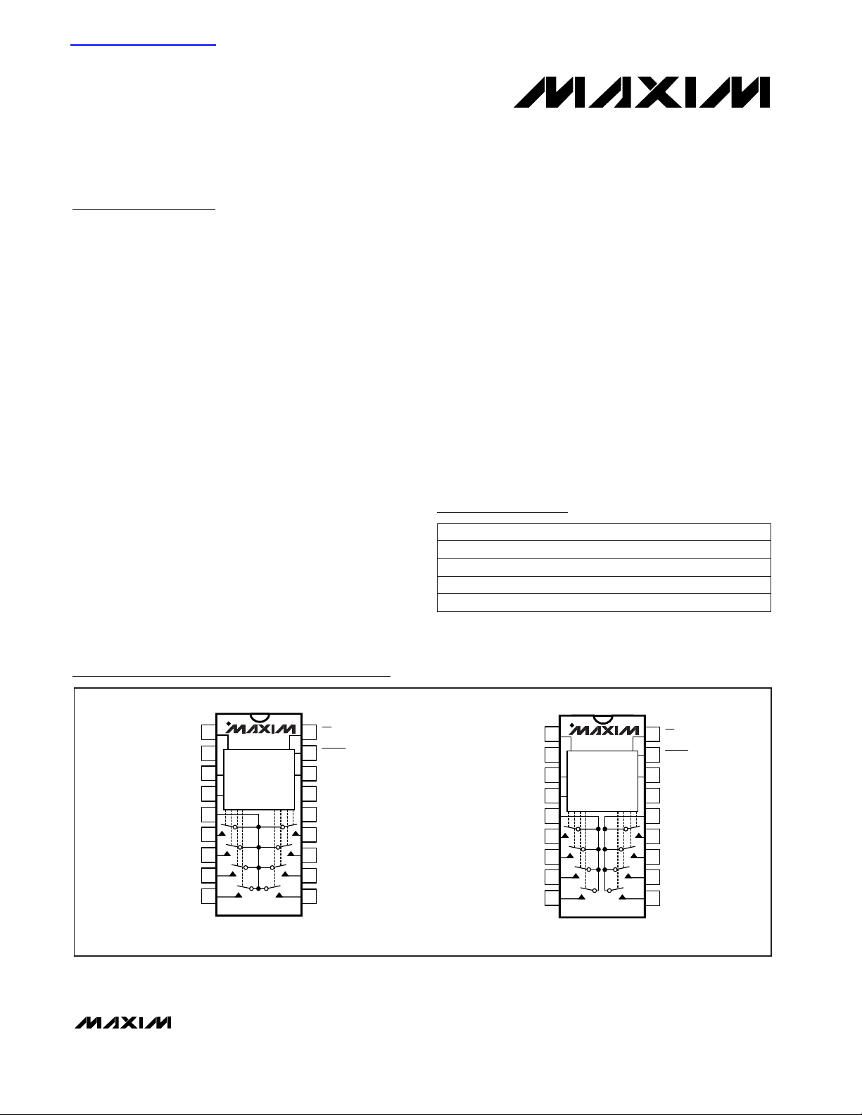
MAX349/MAX350
Serially Controlled, Low-Voltage,
8-Channel/Dual 4-Channel Multiplexers
________________________________________________________________
Maxim Integrated Products
1
18
17
16
15
14
13
12
11
1
2
3
4
5
6
7
8
CS
RESET
DOUT
V-
GND
DIN
V+
SCLK
TOP VIEW
N.C.
NO7
NO6
NO5
NO2
NO1
NO0
COM
10
9
NO4
NO3
DIP/SO
MAX349
LOGIC
18
17
16
15
14
13
12
11
1
2
3
4
5
6
7
8
CS
RESET
DOUT
V-
GND
DIN
V+
SCLK
COMB
NO0B
NO1B
NO2B
NO2A
NO1A
NO0A
COMA
10
9
NO3B
NO3A
DIP/SO
MAX350
LOGIC
N.C. = NOT INTERNALLY
CONNECTED
Pin Configurations/Functional Diagrams
19-0451; Rev 1; 10/98
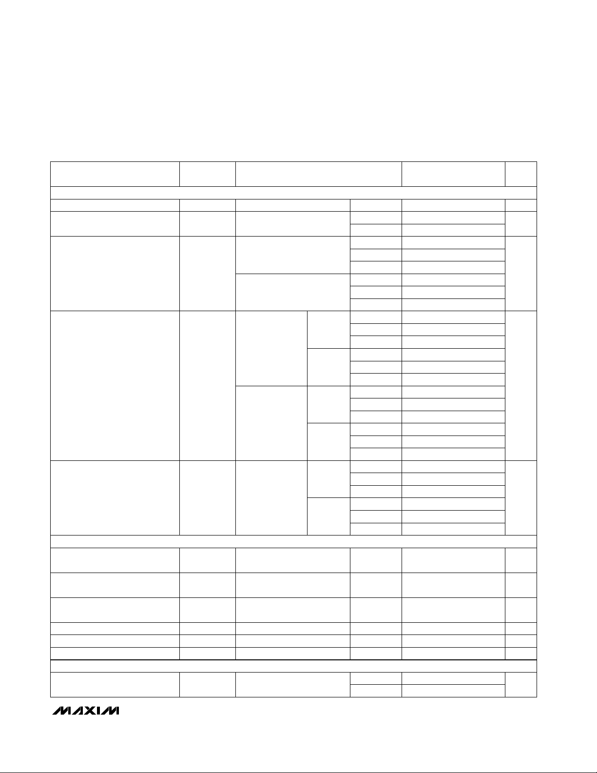
PART
MAX349CPN
MAX349CWN
MAX349CAP 0°C to +70°C
0°C to +70°C
0°C to +70°C
TEMP. RANGE PIN-PACKAGE
18 Plastic DIP
18 Wide SO
20 SSOP
Ordering Information
Ordering Information continued at end of data sheet.
*Contact factory for dice specifications.
MAX349C/D 0°C to +70°C Dice*
Pin Configurations continued at end of data sheet.
SPI and QSPI are trademarks of Motorola, Inc. MICROWIRE is a trademark of National Semiconductor Corp.
Rail-to-Rail is a registered trademark of Nippon Motorola, Ltd.
For free samples & the latest literature: http://www.maxim-ic.com, or phone 1-800-998-8800.
For small orders, phone 1-800-835-8769.
查询MAX349供应商
MAX349/MAX350
Serially Controlled, Low-Voltage,
8-Channel/Dual 4-Channel Multiplexers
2 _______________________________________________________________________________________
ABSOLUTE MAXIMUM RATINGS
ELECTRICAL CHARACTERISTICS—Dual Supplies
(V+ = +4.5V to +5.5V, V- = -4.5V to -5.5V, TA= T
MIN
to T
MAX
, unless otherwise noted. Typical values are at TA= +25°C.)
Stresses beyond those listed under “Absolute Maximum Ratings” may cause permanent damage to the device. These are stress ratings only, and functional
operation of the device at these or any other conditions beyond those indicated in the operational sections of the specifications is not implied. Exposure to
absolute maximum rating conditions for extended periods may affect device reliability.
Voltages Referenced to GND
V+...........................................................................-0.3V, +17V
V-............................................................................-17V, +0.3V
V+ to V-...................................................................-0.3V, +17V
SCLK,
CS, DIN, DOUT, RESET .................-0.3V to (V+ + 0.3V)
NO, COM.................................................(V- - 2V) to (V+ + 2V)
Continuous Current into Any Terminal..............................±30mA
Peak Current, NO or COM
(pulsed at 1ms, 10% duty cycle).................................±100mA
Continuous Power Dissipation (T
A
= +70°C)
18-Pin Plastic DIP (derate 11.11mW/°C above +70°C) ..889mW
18-Pin SO (derate 9.52mW/°C above +70°C)...............762mW
20-Pin SSOP (derate 8.00mW/°C above +70°C) ..........640mW
18-Pin CERDIP (derate 10.53mW/°C above +70°C).....842mW
Operating Temperature Ranges
MAX349C_ _, MAX350C_ _ .................................0°C to +70°C
MAX349E_ _, MAX350E_ _...............................-40°C to +85°C
MAX349M_ _, MAX350M_ _ ...........................-55°C to +125°C
Storage Temperature Range.............................-65°C to +150°C
Lead Temperature (soldering, 10sec).............................+300°C
CONDITIONS UNITS
MIN TYP MAX
(Note 1)
SYMBOLPARAMETER
60 100
VV- V+V
COM
, V
NO
Analog Signal Range
V+ = 5V, V- = -5V,
V
COM
= ±3V, INO= 1mA
Ω
125
R
ON
COM-NO On-Resistance
C, E, M
TA= +25°C
C, E, M
TA= +25°C 16
C, E, M
V+ = 5V, V- = -5V,
V
COM
= ±3V, INO= 1mA
Ω
20
∆R
ON
COM-NO On-Resistance Match
Between Channels (Note 2)
TA= +25°C 10
C, E, M
V+ = 5V, V- = -5V, INO= 1mA,
V
COM
= -3V, 0V, 3V
Ω
15
R
FLAT(ON)
COM-NO On-Resistance
Flatness (Note 2)
TA= +25°C -0.1 0.002 0.1
ANALOG SWITCH
C, E -5 5
V+ = 5.5V, V- = -5.5V,
V
COM
= -4.5V, VNO= 4.5V
M -10 10
TA= +25°C -0.1 0.002 0.1
C, E -5 5
NO Off-Leakage Current
(Note 3)
I
NO(OFF)
V+ = 5.5V, V- = -5.5V,
V
COM
= 4.5V, VNO= -4.5V
M -10 10
nA
TA= +25°C -0.1 0.002 0.1
C, E -10 10
M -100 100
TA= +25°C -0.1 0.002 0.1
C, E -5 5
V+ = 5.5V,
V- = -5.5V,
V
COM
=
±4.5V,
VNO= ±4.5V
M -50 50
TA= +25°C -0.2 0.002 0.2
C, E -10 10
M -100 100
TA= +25°C -0.2 0.002 0.2
C, E -5 5
COM Off-Leakage Current
(Note 3)
I
COM(OFF)
V+ = 5.5V,
V- = -5.5V,
V
COM
=
-4.5V,
VNO= 4.5V
M -50 50
nA
MAX349
MAX349
MAX350
MAX350
MAX349/MAX350
Serially Controlled, Low-Voltage,
8-Channel/Dual 4-Channel Multiplexers
_______________________________________________________________________________________ 3
ELECTRICAL CHARACTERISTICS—Dual Supplies (continued)
(V+ = +4.5V to +5.5V, V- = -4.5V to -5.5V, TA= T
MIN
to T
MAX
, unless otherwise noted. Typical values are at TA= +25°C.)
V2.4C, E, MV
IH
DIN, SCLK, CS, RESET Input
Voltage Logic Threshold High
MAX350
nA
-50 50M
V+ = 5.5V,
V- = -5.5V,
V
COM
= V
NO
=
±4.5V
COM On-Leakage Current
(Note 3)
I
COM(ON)
-5 5C, E
MAX349
-0.2 0.02 0.2TA= +25°C
-100 100M
-10 10C, E
DOUT Output Voltage Logic Low V
DOUT
VI
DOUT
= -1.6mA 0 0.4C, E, M
mV100C, E, M
DOUT Output Voltage Logic High V
DOUT
SCLK
HYST
VI
DOUT
= 0.8mA
SCLK Input Hysteresis
2.8 V+C, E, M
µA-1 0.03 1C, E, M
V
DIN
, V
SCLK
,
VCS= 0.8V or 2.4V
I
IH, IIL
DIN, SCLK, CS, RESET Input
Current Logic High or Low
V0.8C, E, MV
IL
DIN, SCLK, CS, RESET Input
Voltage Logic Threshold Low
-0.2 0.001 0.2TA= +25°C
Turn-On Time t
ON
400
ns
From rising edge of CS
C, E, M
200 275TA= +25°C
-2 2
30
C, E, M
C, E, M
RL= 50Ω, CL= 15pF,
V
NO
= 1V
RMS
, f = 100kHz
Off-Isolation V
ISO
dB
pC
pF
pF
Charge Injection (Note 4)
NO Off-Capacitance
COM Off-Capacitance
V
CTE
C
NO(OFF)
C
COM(OFF)VCOM
= GND, f = 1MHz
CL= 1nF, VNO= 0V, RS= 0Ω
Break-Before-Make Delay t
BBM
2
ns
VNO= GND, f = 1MHz
TA= +25°C
2TA= +25°C
110
From rising edge of CS
TA= +25°C
540TA= +25°C
PARAMETER SYMBOL
MIN TYP MAX
(Note 1)
UNITS
V+ Supply Current I+
720
µA
V- Supply Current I-
-1 0.1 1
µA
Turn-Off Time t
OFF
300
ns
From rising edge of CS
C, E, M
90 150TA= +25°C
DIN = CS = SCLK = 0V or V+,
RESET = 0V or V+
DIN = CS = SCLK = 0V or V+,
RESET = 0V or V+
Channel-to-Channel Crosstalk V
CT
dB< -90
RL= 50Ω, CL= 15pF,
VNO= 1V
RMS
, f = 100kHz
TA= +25°C
Switch On-Capacitance C
(ON)
> 90
C, E, M
TA= +25°C
pF
Power-Supply Range V+, V- ±3 ±8 V
TA= +25°C
8
CONDITIONS
V
COM
= VNO= GND,
f = 1MHz
TA= +25°C
TA= +25°C
DIGITAL I/O
SWITCH DYNAMIC CHARACTERISTICS
POWER SUPPLY
MAX349/MAX350
Serially Controlled, Low-Voltage,
8-Channel/Dual 4-Channel Multiplexers
4 _______________________________________________________________________________________
SCLK Frequency f
SCLK
RESET Minimum Pulse Width
t
RW
70 nsTA= +25°C
Fall Time of DOUT (Note 4) t
DF
100 ns
20% of V+ to 70% of V+,
CL= 10pF
C, E, M
Allowable Fall Time at DIN, SCLK
(Note 4)
t
SCF
2 µs
20% of V+ to 70% of V+,
CL= 10pF
C, E, M
Allowable Rise Time at DIN, SCLK
(Note 4)
t
SCR
2 µs
20% of V+ to 70% of V+,
CL= 10pF
C, E, M
Rise Time of DOUT (Note 4) t
DR
100 ns
20% of V+ to 70% of V+,
CL= 10pF
C, E, M
DIN Data Valid after Falling SCLK
(Note 4)
t
DO
400
ns
Data Hold Time
Minimum Data Setup Time t
DS
17 100 ns
t
DH
0 -17
85
50% of SCLK to 10% of DOUT,
CL= 10pF
SCLK Low Time
ns
t
CL
C, E, M
190 ns
TA= +25°C
C, E, M
C, E, M
PARAMETER SYMBOL
MIN TYP MAX
(Note 1)
UNITS
C, E, M
SCLK High Time
CS Lag Time
t
CSH2
240 ns
t
CH
190
CS Lead Time
Cycle Time
ns
t
CH +tCL
480
t
CSS
240 ns
C, E, M
0 2.1nsMHz
C, E, M
C, E, M
C, E, M
C, E, M
CONDITIONS
SERIAL DIGITAL INTERFACE
TIMING CHARACTERISTICS—Dual Supplies (Figure 1)
(V+ = +4.5V to +5.5V, V- = -4.5V to -5.5V, TA= T
MIN
to T
MAX
, unless otherwise noted. Typical values are at TA= +25°C.)
Note 1: The algebraic convention is used in this data sheet; the most negative value is shown in the minimum column.
Note 2: ∆R
ON
= R
ON(max)
- R
ON(min)
. On-resistance match between channels and on-resistance flatness are guaranteed only with
specified voltages. Flatness is defined as the difference between the maximum and minimum value of on-resistance as
measured over the specified analog signal range.
Note 3: Leakage parameters are 100% tested at maximum rated hot temperature and guaranteed by correlation at room temp.
Note 4: Guaranteed by design.
Note 5: Leakage testing at single supply is guaranteed by testing with dual supplies.
Note 6: See Figure 6. Off-isolation = 20log
10VCOM/VNO
, V
COM
= output. NO = input to off switch.
Note 7: Between any two switches. See Figure 3.
MAX349/MAX350
Serially Controlled, Low-Voltage,
8-Channel/Dual 4-Channel Multiplexers
_______________________________________________________________________________________ 5
ELECTRICAL CHARACTERISTICS—Single +5V Supply
(V+ = +4.5V to +5.5V, V- = 0V, TA= T
MIN
to T
MAX
, unless otherwise noted. Typical values are at TA= +25°C.)
TA= +25°C
C, E, M
125 175
C, E, M
VV- V+V
COM
, V
NO
Analog Signal Range
TA= +25°C -0.1 0.002 0.1
TA= +25°C -0.2 0.002 0.2
C, E
C, E
CONDITIONS
-10 10
-10 10
V+ = 5V, V
COM
= 3.5V,
INO= 1mA
M -100 100
TA= +25°C
M -100 100
TA= +25°C -0.2 0.002 0.2
MAX349
C, E -5 5
M
Ω
225
R
ON
COM-NO On-Resistance
-50 50
-0.1 0.002 0.1
nA
V+ = 5.5V,
V
COM
= 0V,
VNO= 4.5V
MAX350
I
COM(OFF)
COM Off-Leakage Current
(Notes 4, 5)
TA= +25°C -0.2 0.01 0.2
C, E -10 10
M -100 100
TA= +25°C -0.2 0.02 0.2
MAX349
C, E -5 5
M
MAX349
-50 50
C, E -5 5
M -50 50
V+ = 5.5V,
V
COM
= VNO=
±4.5V
nA
MAX350
V+ = 5.5V,
V
COM
= 4.5V,
VNO= 0V
I
COM(ON)
COM On-Leakage Current
(Notes 4, 5)
MAX350
UNITS
MIN TYP MAX
(Note 1)
SYMBOLPARAMETER
TA= +25°C -0.1 0.002 0.1
C, E -5 5
M
V+ = 5.5V, V
COM
= 4.5V,
VNO= 0V
-10 10
C, E, M 2.4
C, E, M 0.8V
IL
V
IH
DIN, SCLK, CS, RESET Input
Voltage Logic Threshold Low
DIN, SCLK, CS, RESET Input
Voltage Logic Threshold High
V
V
C, E, M -1 0.03 1
C, E, M 2.8 V+
C, E, M 0 0.4I
DOUT
= -1.6mA
I
DOUT
= 0.8mA
V
DIN
, V
SCLK
,
VCS= 0.8V or 2.4V
V
DOUT
V
DOUT
IIH, I
IL
DOUT Output Voltage Logic Low
DOUT Output Voltage Logic High
DIN, SCLK, CS, RESET Input
Current Logic High or Low
V
V
µA
C, E, M 100SCLK
HYST
SCLK Input Hysteresis mV
TA= +25°C 720
C, E, M 30
DIN = CS = SCLK = 0V or V+,
RESET = 0V or V+
I+V+ Supply Current µA
TA= +25°C -0.1 0.002 0.1
C, E -5 5
M
V+ = 5.5V, V
COM
= 0V,
VNO= 4.5V
nA
-10 10
I
NO(OFF)
NO Off-Leakage Current
(Notes 4, 5)
DIGITAL I/O
ANALOG SWITCH
POWER SUPPLY
MAX349/MAX350
Serially Controlled, Low-Voltage,
8-Channel/Dual 4-Channel Multiplexers
6 _______________________________________________________________________________________
ELECTRICAL CHARACTERISTICS—Single +5V Supply (continued)
(V+ = +4.5V to +5.5V, V- = 0V, TA= T
MIN
to T
MAX
, unless otherwise noted. Typical values are at TA= +25°C.)
CL= 1nF, VNO= 0V, RS= 0ΩV
CTE
Charge Injection (Note 4) pC
dB
CONDITIONS
TA= +25°C
TA= +25°C
160 400
> 90
TA= +25°C
RL= 50Ω, CL= 15pF,
VNO= 1V
RMS
, f = 100kHz
< -90
C, E, M
From rising edge of CS
ns
dB
V
ISO
V
CT
Channel-to-Channel Crosstalk
(Note 7)
Off-Isolation (Note 6)
RL= 50Ω, CL= 15pF,
VNO= 1V
RMS
, f = 100kHz
500
t
ON
Turn-On Time
TA= +25°C 60 200
C, E, M
From rising edge of CS
ns
300
t
OFF
Turn-Off Time
UNITS
MIN TYP MAX
(Note 1)
SYMBOLPARAMETER
TA= +25°C
15
TA= +25°C
From rising edge of CS
110
ns
t
BBM
Break-Before-Make Delay
SWITCH DYNAMIC CHARACTERISTICS

MAX349/MAX350
Serially Controlled, Low-Voltage,
8-Channel/Dual 4-Channel Multiplexers
_______________________________________________________________________________________ 7
TIMING CHARACTERISTICS—Single +5V Supply (Figure 1)
(V+ = +4.5V to +5.5V, V- = 0V, TA= T
MIN
to T
MAX
, unless otherwise noted. Typical values are at TA= +25°C.)
SERIAL DIGITAL INTERFACESERIAL DIGITAL INTERFACE
Rise Time of DOUT (Note 4) t
DR
100 ns
20% of V+ to 70% of V+,
CL= 10pF
C, E, M
Allowable Fall Time at DIN,
SCLK (Note 4)
t
SCF
2 µs
20% of V+ to 70% of V+,
CL= 10pF
C, E, M
Allowable Rise Time at DIN,
SCLK (Note 4)
t
SCR
2 µs
20% of V+ to 70% of V+,
CL= 10pF
C, E, M
DIN Data Valid after Falling SCLK
(Note 4)
t
DO
400
ns
Data Hold Time (Note 4)
Minimum Data Setup Time
(Note 4)
t
DS
17 100 ns
t
DH
-17
85
50% of SCLK to 10% of
DOUT, CL= 10pF
SCLK Low Time (Note 4)
ns
t
CL
C, E, M
190 ns
TA= +25°C
C, E, M
C, E, M
PARAMETER SYMBOL
MIN TYP MAX
(Note 1)
UNITS
C, E, M
SCLK High Time (Note 4)
CS Lag Time (Note 4)
t
CSH2
240 ns
t
CH
190
CS Lead Time (Note 4)
Cycle Time (Note 4)
SCLK Frequency f
SCLK
ns
0 2.1 MHz
t
CH +tCL
480
t
CSS
240 ns
C, E, M
ns
C, E, M
C, E, M
C, E, M
C, E, M
CONDITIONS
C, E, M
20% of V+ to 70% of V+,
CL= 10pF
ns100t
DF
Fall Time of DOUT (Note 4)
Note 1: The algebraic convention is used in this data sheet; the most negative value is shown in the minimum column.
Note 2: ∆R
ON
= R
ON(max)
- R
ON(min)
. On-resistance match between channels and on-resistance flatness are guaranteed only with
specified voltages. Flatness is defined as the difference between the maximum and minimum value of on-resistance as
measured over the specified analog signal range.
Note 3: Leakage parameters are 100% tested at maximum rated hot temperature and guaranteed by correlation at room temp.
Note 4: Guaranteed by design.
Note 5: Leakage testing at single supply is guaranteed by testing with dual supplies.
Note 6: See Figure 6. Off-isolation = 20log
10VCOM/VNO
, V
COM
= output. NO = input to off switch.
Note 7: Between any two switches. See Figure 3.
RESET Minimum Pulse Width
t
RW
70 nsTA= +25°C

MAX349/MAX350
Serially Controlled, Low-Voltage,
8-Channel/Dual 4-Channel Multiplexers
8 _______________________________________________________________________________________
V
ELECTRICAL CHARACTERISTICS—Single +3V Supply
(V+ = +3.0V to +3.6V, V- = 0V, TA= T
MIN
to T
MAX
, unless otherwise noted. Typical values are at TA= +25°C.)
TA= +25°C
C, E, M
270 500
C, E, M
C, E, M 100
VV- V+V
COM
, V
NO
C, E 2.4
Analog Signal Range
TA= +25°C -0.1 0.002 0.1
TA= +25°C -0.2 0.002 0.2
C, E
C, E
CONDITIONS
-10 10
-10 10
V+ = 3.0V, V
COM
= 1.5V,
INO= 1mA
M -100 100
TA= +25°C
M -100 100
TA= +25°C -0.2 0.002 0.2
C, E 0.8
MAX349
C, E -5 5
M
Ω
600
R
ON
COM-NO On-Resistance
-50 50
-0.1 0.002 0.1
nA
V+ = 3.6V,
V
COM
= 0V,
VNO= 3V
SCLK
HYST
MAX350
I
COM(OFF)
COM Off-Leakage Current
(Notes 4, 5)
TA= +25°C -0.2 0.01 0.2
C, E -10 10
M -100 100
TA= +25°C
SCLK Input Hysteresis
-0.2 0.02 0.2
MAX349
mV
C, E -5 5
M
V
IL
V
IH
MAX349
-50 50
C, E -5 5
M -50 50
V+ = 3.6V,
V
COM
= VNO= 3V
nA
MAX350
V+ = 3.6V,
V
COM
= 3V,
VNO= 0V
I
COM(ON)
COM On-Leakage Current
(Notes 4, 5)
DIN, SCLK, CS, RESET Input
Voltage Logic Threshold Low
DIN, SCLK, CS, RESET Input
Voltage Logic Threshold High
V
V
C, E -1 0.03 1
C, E, M 2.8 V+
C, E, M
MAX350
0 0.4
UNITS
MIN TYP MAX
(Note 1)
SYMBOLPARAMETER
I
DOUT
= -1.6mA
I
DOUT
= 0.1mA
V
DIN
, V
SCLK
,
VCS= 0.8V or 2.4V
V
DOUT
V
DOUT
IIH, I
IL
DOUT Output Voltage Logic Low
DOUT Output Voltage Logic High
DIN, SCLK, CS, RESET Input
Current Logic High or Low
V
V
µA
C, E, M 30
DIN = CS = SCLK = 0V or V+,
RESET = 0V or 5V
I+V+ Supply Current µA
TA= +25°C 620
DIGITAL I/O
ANALOG SWITCH
POWER SUPPLY

MAX349/MAX350
Serially Controlled, Low-Voltage,
8-Channel/Dual 4-Channel Multiplexers
_______________________________________________________________________________________ 9
MAX349/MAX350
ELECTRICAL CHARACTERISTICS—Single +3V Supply (continued)
(V+ = +3.0V to +3.6V, V- = 0V, TA= T
MIN
to T
MAX
, unless otherwise noted. Typical values are at TA= +25°C.)
SWITCH DYNAMIC CHARACTERISTICS
Break-Before-Make Delay (Note 4) t
BBM
ns
110
From rising edge of CS
TA= +25°C
515TA= +25°C
PARAMETER SYMBOL
MIN TYP MAX
(Note 1)
UNITS
Turn-Off Time (Note 4) t
OFF
400
ns
From rising edge of CS
C, E, M
120 300TA= +25°C
Turn-On Time (Note 4) t
ON
700
RL= 50Ω, CL= 15pF,
VNO= 1V
RMS
, f = 100kHz
Off-Isolation (Note 6)
Channel-to-Channel Crosstalk
(Note 7)
V
CT
V
ISO
dB
ns
From rising edge of CS
C, E, M
< –90
RL= 50Ω, CL= 15pF,
VNO= 1V
RMS
, f = 100kHz
TA= +25°C
> 90
275 600TA= +25°C
TA= +25°C
CONDITIONS
dB
pCCharge Injection (Note 4) V
CTE
CL= 1nF, VNO= 0V, RS= 0Ω

Note 1: The algebraic convention is used in this data sheet; the most negative value is shown in the minimum column.
Note 2: ∆R
ON
= R
ON(max)
- R
ON(min)
. On-resistance match between channels and on-resistance flatness are guaranteed only with
specified voltages. Flatness is defined as the difference between the maximum and minimum value of on-resistance as
measured over the specified analog signal range.
Note 3: Leakage parameters are 100% tested at maximum rated hot temperature and guaranteed by correlation at room temp.
Note 4: Guaranteed by design.
Note 5: Leakage testing at single supply is guaranteed by testing with dual supplies.
Note 6: See Figure 6. Off-isolation = 20log
10VCOM/VNO
, V
COM
= output. NO = input to off switch.
Note 7: Between any two switches. See Figure 3.
MAX349/MAX350
Serially Controlled, Low-Voltage,
8-Channel/Dual 4-Channel Multiplexers
10 ______________________________________________________________________________________
TIMING CHARACTERISTICS—Single +3V Supply (Figure 1)
(V+ = +3.0V to +3.6V, V- = 0V, TA= T
MIN
to T
MAX
, unless otherwise noted. Typical values are at TA= +25°C.)
SERIAL DIGITAL INTERFACE
RESET Minimum Pulse Width
(Note 4)
t
RW
105 nsTA= +25°C
Allowable Fall Time at DIN, SCLK
(Note 4)
t
SCF
2 µs
20% of V+ to 70% of V+,
CL= 10pF
C, E, M
Fall Time of DOUT (Note 4) t
DF
100 ns
20% of V+ to 70% of V+,
CL= 10pF
C, E, M
Rise Time of DOUT (Note 4) t
DR
100 ns
20% of V+ to 70% of V+,
CL= 10pF
C, E, M
Allowable Rise Time at DIN,
SCLK (Note 4)
t
SCR
2 µs
20% of V+ to 70% of V+,
CL= 10pF
C, E, M
DIN Data Valid after Falling SCLK
(Note 4)
t
DO
400
ns
Data Hold Time (Note 4)
Minimum Data Setup Time
(Note 4)
t
DS
38 120 ns
t
DH
-38
150
50% of SCLK to 10% of
DOUT, CL= 10pF
SCLK Low Time (Note 4)
ns
t
CL
C, E, M
190 ns
TA= +25°C
C, E, M
C, E, M
PARAMETER SYMBOL
MIN TYP MAX
(Note 1)
UNITS
C, E, M
SCLK High Time (Note 4)
CS Lag Time (Note 4) t
CSH2
240 ns
t
CH
190
CS Lead Time (Note 4)
Cycle Time (Note 4)
SCLK Frequency f
SCLK
ns
0 2.1 MHz
t
CH +tCL
480
t
CSS
240 ns
C, E, M
ns
C, E, M
C, E, M
C, E, M
C, E, M
CONDITIONS

MAX349/MAX350
Serially Controlled, Low-Voltage,
8-Channel/Dual 4-Channel Multiplexers
______________________________________________________________________________________
11
0
-5 -3 1
ON-RESISTANCE vs. V
COM
(DUAL SUPPLIES)
40
120
MAX349/350-TOC1
V
COM
(V)
R
ON
(Ω)
-1 3
80
140
20
100
60
5-4 0-2 2 4
V± = ±5V
V± = ±3V
V± = ±2.5V
110
30
-5 -3 1
ON-RESISTANCE vs. V
COM
AND TEMPERATURE
(DUAL SUPPLIES)
50
90
MAX349/350-TOC2
V
COM
(V)
R
ON
(Ω)
-1 3
70
100
40
80
60
5-4 0-2 2 4
V± = ±5.5V
TA = +125°C
TA = +85°C
TA = +25°C
TA = -55°C
0
04
ON-RESISTANCE vs. V
COM
(SINGLE SUPPLY)
100
300
MAX349/350-TOC3
V
COM
(V)
R
ON
(Ω)
8
200
400
350
50
250
150
210126
V+ = 3V
V+ = 12V
V+ = 5V
V+ = 2.5V
V- = 0V
V+ = 9V
180
02
ON-RESISTANCE vs. V
COM
AND TEMPERATURE
(SINGLE SUPPLY)
100
MAX349/350-TOC4
V
COM
(V)
R
ON
(Ω)
4
60
140
160
120
80
40
153
TA = +25°C
TA = -55°C
TA = +85°C
TA = +125°C
V+ = 5V
V- = 0V
0.1
OFF-LEAKAGE vs.
TEMPERATURE
1,000
MAX349/350-TOC5
TEMPERATURE (°C)
OFF-LEAKAGE (pA)
10
1
100
-50 12525-25 0 7550 100
V± = ±5.5V
0.1
ON-LEAKAGE vs.
TEMPERATURE
1,000
10,000
MAX349/350-TOC6
TEMPERATURE (°C)
ON-LEAKAGE (pA)
10
1
100
-50 12525-25 0 7550 100
V± = ±5.5V
__________________________________________Typical Operating Characteristics
(V+ = +5V, V- = -5V, GND = 0V, TA = +25°C, unless otherwise noted.)
-5 -3 1
CHARGE INJECTION vs. V
COM
-5
5
MAX349/350-TOC7
V
COM
(V)
V
CTE
(pC)
-1 3
-4
4
-3
3
-2
2
-1
1
0
5-4 0-2 2 4
A: V+ = 5V, V- = -5V
B: V+ = 5V, V- = 0V
A
B
-5 -3 1
TURN-ON/TURN-OFF TIMES vs. V
COM
0
250
MAX349/350-TOC8
V
COM
(V)
t
ON
, t
OFF
(ns)
-1 3
50
200
100
150
5-4 0-2 2 4
A = t
ON
A: V+ = 5V, V- = 5V
B: V+ = 5V, V- = 0V
A = t
OFF
B = t
OFF
B = t
ON
-50
04
DATA HOLD TIME vs.
POWER-SUPPLY VOLTAGE
-30
10
MAX349/350-TOC9
SUPPLY VOLTAGE (V)
DATA HOLD TIME (ns)
8
-10
30
40
50
20
-40
0
-20
26

MAX349/MAX350
Serially Controlled, Low-Voltage,
8-Channel/Dual 4-Channel Multiplexers
12 ______________________________________________________________________________________
0
04
DATA SETUP TIME vs.
POSITIVE SUPPLY VOLTAGE
20
60
MAX349/350-TOC10
SUPPLY VOLTAGE (V)
DATA SETUP TIME (ns)
8
40
80
90
100
70
10
50
30
26
100
0.001
-50 125
POWER-SUPPLY CURRENT
vs. TEMPERATURE
10
1
MAX349/350-TOC11
TEMPERATURE (°C)
I+, I-, (µA)
25
0.1
0.01
-25 0 7550
100
V± = ±5.5V
I+
I-
10
04
MINIMUM SCLK PULSE WIDTH vs.
POSITIVE SUPPLY VOLTAGE
15
25
MAX349/350-TOC12
SUPPLY VOLTAGE (V)
SCLK (ns)
8
20
30
35
26
0
-100
10k 100k 10M 1G
FREQUENCY RESPONSE
-80
-20
MAX349/350 TOC13
FREQUENCY (Hz)
LOSS (dB)
PHASE (DEGREES)
1M 100M
-40
-60
20
-80
-100
-120
-60
0
-20
-40
PHASE
OFF ISOLATION
INSERTION LOSS
ISOLATION OF
A BARE SOCKET
V± = ±5V
50W IN AND OUT
0.01
10 100 1k 10k
TOTAL HARMONIC DISTORTION
vs. FREQUENCY
0.1
MAX349/350-TOC14
FREQUENCY (Hz)
TDH (%)
1
10
100
V± = ±5V
600Ω IN AND OUT
Typical Operating Characteristics (continued)
(V+ = +5V, V- = -5V, GND = 0V, TA = +25°C, unless otherwise noted.)

MAX349/MAX350
Serially Controlled, Low-Voltage,
8-Channel/Dual 4-Channel Multiplexers
______________________________________________________________________________________ 13
Pin Description
Note: NO and COM pins are identical and interchangeable. Either may be considered as an input or an output; signals pass equally
well in either direction.
• • •
• • •
• • •
• • •
• • •
SCLK
DIN
DOUT
COM-OUT
CS
t
DO
t
DH
t
DS
t
CSS
t
CH
t
CL
t
CSH2
tON,
t
OFF
• • •
Figure 1. Timing Diagram
1 Serial Clock Digital Input
2 Positive Analog Supply Voltage Input
3 Serial Data Digital Input
5 Common Analog Switch (mux output)
6–13 Normally Open Analog Switch Inputs 0–7
— Common Analog Switch “A” (mux output)
— Normally Open Analog Switch “A” Inputs 0–3
— Normally Open Analog Switch “B” Inputs 0–3
— Common Analog Switch “B” (mux output)
4
Ground. Connect to digital ground. (Analog signals have
no ground reference; they are limited to V+ and V-.)
1 SCLK
2 V+
3 DIN
5 COM
6–9, 11–14 NO0–NO7
— COMA
— NO0A–NO3A
— NO3B–NO0B
— COMB
4 GND
15
Negative Analog Supply Voltage Input. Connect to GND
for single-supply operation.
16 Serial Data Digital Output. Output high is V+.
17
RESET Input. Connect to logic high (or V+) for normal operation.
Drive low to set all switches off and set internal shift registers to 0.
18 Chip-Select Digital Input (Figure 1)
17 V18 DOUT
19
RESET
20
CS
14 No Connect, not internally connected.10, 15, 16 N.C.
MAX349
SSOPDIP/SO
NAME FUNCTION
1
2
3
—
—
5
6–9
10–13
14
4
1
2
3
—
—
5
6–9
11–14
15
4
15
16
17
18
17
18
19
20
— 10, 16
MAX350
SSOPDIP/SO
PIN

MAX349/MAX350
Serially Controlled, Low-Voltage,
8-Channel/Dual 4-Channel Multiplexers
14 ______________________________________________________________________________________
Detailed Description
Basic Operation
The MAX349/MAX350 are 8-channel and dual 4-channel, serially controlled multiplexers (muxes). These
muxes are unusual in that any, all, or none of the input
channels can be directed to the output. All switches
are bidirectional, so inputs and outputs are interchangeable. When multiple inputs are connected to an
output, they are also connected to one another, separated from each other only by the on-resistance of two
switches. Both parts require eight bits of serial data to
set all eight switches.
Serial Digital Interface
The MAX349/MAX350 interface can be thought of as an
8-bit shift register controlled by CS (Figure 2). While CS
is low, input data appearing at DIN is clocked into the
shift register synchronously with SCLK’s rising edge.
The input is an 8-bit word, each bit controlling one of
the eight switches (Tables 1 and 2). DOUT is the output
of the shift register, with data appearing synchronously
with SCLK’s falling edge. Data at DOUT is simply the
input data delayed by eight clock cycles.
When shifting the input data, D7 is the first bit in and
out of the shift register. While shifting data, the switches
remain in their previous configuration. When the eight
bits of data have been shifted in, CS is driven high.
This updates the new switch configuration and inhibits
further data from entering the shift register. Transitions
at DIN and SCLK have no effect when CS is high, and
DOUT holds the first input bit (D7) at its output.
More or fewer than eight clock cycles can be entered
during the CS low period. When this happens, the shift
register contains only the last eight serial data bits,
regardless of when they were entered. On the rising
edge of CS, all switches are set to the corresponding
states.
The MAX349/MAX350 three-wire serial interface is
compatible with SPI, QSPI, and MICROWIRE standards.
If interfacing with a Motorola processor serial interface,
set CPOL = 0. The MAX349/MAX350 are considered to
be slave devices (Figures 2 and 3). At power-up, the
shift register contains all zeros, and all switches are off.
The latch that drives the analog switch is updated on
the rising edge of CS, regardless of SCLK’s state. This
meets all SPI and QSPI requirements.
Daisy-Chaining
For a simple interface using several MAX349s and
MAX350s, “daisy-chain” the shift registers as shown in
Figure 5. The CS pins of all devices are connected,
and a stream of data is shifted through the MAX349s or
MAX350s in series. When CS is brought high, all
switches are updated simultaneously. Additional shift
registers may be included anywhere in series with the
MAX349/MAX350 data chain. Note that the DOUT high
level is V+, which may not be compatible with
TTL/CMOS devices if V+ differs from the logic supply
for these other devices.
Addressable Serial Interface
When several serial devices are configured as slaves,
addressable by the processor, DIN pins of each
decode logic individually control CS of each slave
device. When a slave is selected, its CS pin is driven
low, data is shifted in, and CS is driven high to latch the
data. Typically, only one slave is addressed at a time.
DOUT is not used.
Applications Information
8x1 Multiplexer
The MAX349 can be programmed normally, with only
one channel selected for every eight clock pulses, or it
can be programmed in a fast mode, where channel
changing occurs on each clock pulse.
In fast mode, select the channels by sending a single high
pulse (corresponding to the selected channel) at DIN, and
a corresponding CS low pulse for every eight clock pulses. As SCLK clocks this through the register, each switch
sequences one channel at a time, starting with channel 0.
D7 D6 D5 D4
MSB
LSB
D3 D2 D1 D0
DATA BITS FROM PREVIOUS DATA INPUT
DOUT POWER-UP DEFAULT: D7–D0 = 0
D6 D5 D4 D3 D2 D1 D0
D7
DOUT
DIN
SCLK
SWITCHES UPDATED
DATA CLOCKED IN
DATA CLOCKED OUT
CS
D7
INPUT DATA BITS
Figure 2. 3-Wire Interface Timing

Table 2. MAX350 Serial-Interface Switch Programming
Serially Controlled, Low-Voltage,
8-Channel/Dual 4-Channel Multiplexers
MAX349/MAX350
______________________________________________________________________________________ 15
X = Don’t care. Data bit D7 is first bit in; data bit D0 is last in.
X1 Switch 0 open (off)X XX X
0
XX
X
MAX349 FUNCTION
XX XX1
1
X
DATA BITS
Switch 0 closed to COM
X
0
01
0
1
11
All switches open, D7–D0 = 0
Switch 7 open (off)
All switches closed to COM, D7–D0 = 1
All switches open, D7–D0 = 0
X
X1
X1
X1
1
1
Switch 6 open (off)
Switch 5 open (off)
Switch 6 closed to COM
Switch 7 closed to COM
X1
X1
X1
X1
Switch 4 open (off)
Switch 3 open (off)
Switch 4 closed to COM
Switch 5 closed to COM
X1
X1
X1
X1
Switch 2 open (off)
Switch 1 open (off)
Switch 2 closed to COM
Switch 3 closed to COM
D7
0
X
1
X
0
X
1
X
X
X
X
X
X
X
X
X
D6
0 0
XX
1
X
1
X
X
X
X
0
X
1
X
X
X
X
X
D4
X
X
0
X
X
X
X
X
1
X
X
X
X
D5
0 0
XX
1
X
1
X
X
X
X
X
X
X
X
0
X
1
X
D2
0 0
XX
1
X
1
RESET
X
X
X
X
X
X
X
X
X
X
X
X
X
X
X
D0
X
X
X
X
X
X
X
X
X
X
X
0
X
X
D1
X
X
0
X
X
X
X
X
1
D3
X XX XX1 X
1
Switch 1 closed to COMX
Table 1. MAX349 Serial-Interface Switch Programming
X1 Switch NO0A open (off)X XX X
0
XX
X
MAX350 FUNCTION
XX XX1
1
X
DATA BITS
Switch NO0A closed
X
0
01
0
1
11
All switches open, D7–D0 = 0
Switch NO0B open (off)
All “A” switches closed to COMA; All “B”
switches closed to COMB, D7–D0 = 1
All switches open, D7–D0 = 0
X
X1
X1
X1
1
1
Switch NO1B open (off)
Switch NO2B open (off)
Switch NO1B closed
Switch NO0B closed
X1
X1
X1
X1
Switch NO3B open (off)
Switch NO3A open (off)
Switch NO3B closed
Switch NO2B closed
X1
X1
X1
X1
Switch NO2A open (off)
Switch NO1A open (off)
Switch NO2A closed
Switch NO3A closed
D7
0
X
1
X
0
X
1
X
X
X
X
X
X
X
X
X
D6
0 0
XX
1
X
1
X
X
X
X
0
X
1
X
X
X
X
X
D4
X
X
0
X
X
X
X
X
1
X
X
X
X
D5
0 0
XX
1
X
1
X
X
X
X
X
X
X
X
0
X
1
X
D2
0 0
XX
1
X
1
RESET
X
X
X
X
X
X
X
X
X
X
X
X
X
X
X
D0
X
X
X
X
X
X
X
X
X
X
X
0
X
X
D1
X
X
0
X
X
X
X
X
1
D3
X XX XX1 X
1
Switch NO1A closed X

MAX349/MAX350
Serially Controlled, Low-Voltage,
8-Channel/Dual 4-Channel Multiplexers
16 ______________________________________________________________________________________
SCLK
DIN
DOUT
CS
SK
SO
SI
I/O
MICROWIRE
PORT
MAX349
MAX350
THE DOUT-SI CONNECTION IS NOT REQUIRED FOR WRITING TO THE
MAX349/MAX350, BUT MAY BE USED FOR DATA-ECHO PURPOSES.
Figure 3. Connections for MICROWIRE
DOUT
DIN
SCLK
CS
MISO
MOSI
SCK
I/O
SPI
PORT
MAX349
MAX350
THE DOUT-MISO CONNECTION IS NOT REQUIRED FOR WRITING TO THE
MAX349/MAX350, BUT MAY BE USED FOR DATA-ECHO PURPOSES.
CPOL = 0, CPHA = 0
Figure 4. Connections for SPI and QSPI
SCLK
DIN
CS
MAX349
MAX350
SCLK
DIN
CS
MAX349
MAX350
SCLK
DIN
CS
MAX349
MAX350
DOUT DOUT DOUT
SCLK
DIN
CS
TO OTHER
SERIAL DEVICES
Figure 5. Daisy-Chained Connection
Dual, Differential 4-Channel Multiplexer
The MAX350 can be programmed normally, with only
one differential channel selected for every eight clock
pulses, or it can be programmed in a fast mode, where
channel changing occurs on each clock pulse.
In fast mode, select the channels by sending two high
pulses, spaced four clock pulses apart (corresponding
to the two selected channels) at DIN, and a corresponding CS low pulse for each of the first eight clock
pulses. As SCLK clocks this through the register, each
switch sequences one differential channel at a time,
starting with channel 0. Repeat this process for subse-
quent channel sequencing after the first eight bits have
been sent. For even faster channel sequencing, send
only one DIN high pulse and one CS
low pulse for
every four clock pulses.
Reset Function
RESET is the internal reset pin. It is usually connected
to a logic signal or V+. Drive RESET low to open all
switches and set the contents of the internal shift register to zero simultaneously. When RESET is high, the
part functions normally and DOUT is sourced from V+.
RESET must not be driven beyond V+ or GND.

Power-Supply Considerations
Overview
The MAX349/MAX350 construction is typical of most
CMOS analog switches. It has three supply pins: V+, Vand GND. V+ and V- are used to drive the internal
CMOS switches, and they set the limits of the analog
voltage on any switch. Reverse ESD-protection diodes
are internally connected between each analog signal
pin and both V+ and V-. If any analog signal exceeds
V+ or V-, one of these diodes will conduct. During normal
operation, these (and other) reverse-biased ESD diodes
leak, forming the only current drawn from V+ or V-.
Virtually all the analog leakage current is through the
ESD diodes. Although the ESD diodes on a given signal pin are identical, and therefore fairly well balanced,
they are reverse biased differently. Each is biased by
either V+ or V- and the analog signal. This means their
leakages vary as the signal varies. The
difference
in the
two diode leakages to the V+ and V- pins constitutes
the analog signal-path leakage current. All analog leakage current flows to the supply terminals, not to the
other switch terminal. This is why both sides of a given
switch can show leakage currents of either the same or
opposite polarity.
There is no connection between the analog signal
paths and GND.
V+ and GND power the internal logic and logic-level
translators, and set both the input and output logic limits. The logic-level translators convert the logic levels to
switched V+ and V- signals to drive the analog signal
gates. This drive signal is the only connection between
the logic supplies (and signals) and the analog supplies. V+ and V- have ESD-protection diodes to GND.
The logic-level inputs and output have ESD protection
to V+ and to GND.
The logic-level thresholds are CMOS and TTL compatible when V+ is +5V. As V+ rises, the threshold increases
slightly. Therefore, when V+ reaches +12V, the threshold
is about 3.1V; above the TTL-guaranteed high-level minimum of 2.8V, but still compatible with CMOS outputs.
MAX349/MAX350
Serially Controlled, Low-Voltage,
8-Channel/Dual 4-Channel Multiplexers
______________________________________________________________________________________ 17
FOUR CLOCK
PULSES
DIN
SCLK
D4
SW4
D0
SW0
Figure 7. Differential Multiplexer Input Control
CS
SCLK
DIN
MAX349
MAX350
CS
SCLK
DIN
MAX349
MAX350
CS
SCLK
DIN
MAX349
MAX350
TO OTHER
SERIAL
DEVICES
DIN
SCLK
CS1
CS2
CS3
Figure 6. Addressable Serial Interface

MAX349/MAX350
Serially Controlled, Low-Voltage,
8-Channel/Dual 4-Channel Multiplexers
18 ______________________________________________________________________________________
Pin Configurations/Functional Diagrams (continued)
20
19
18
17
16
15
14
13
1
2
3
4
5
6
7
8
CS
TOP VIEW
RESET
DOUT
V-
GND
DIN
V+
SCLK
N.C.
N.C.
NO7
NO6
NO2
NO1
NO0
COM
12
11
9
10
NO5
NO4
N.C.
NO3
SSOP
MAX349
20
19
18
17
16
15
14
13
1
2
3
4
5
6
7
8
CS
RESET
DOUT
V-
GND
DIN
V+
SCLK
N.C.
N.C. = NOT INTERNALLY CONNECTED
COMB
NO0B
NO1B
NO2A
NO1A
NO0A
COMA
12
11
9
10
NO2B
NO3B
N.C.
NO3A
SSOP
LOGIC
LOGIC
MAX350
Bipolar Supplies
The MAX349/MAX350 operate with bipolar supplies
from ±3.0V and ±8V. The V+ and V- supplies need not
be symmetrical, but their sum cannot exceed the
absolute maximum rating of 17V. Do not connect the
MAX349/MAX350 V+ to +3V and connect the logiclevel pins to TTL logic-level signals. This exceeds
the absolute maximum ratings and can damage the
part and/or external circuits.
Single Supply
The MAX349/MAX350 operate from single supplies
between +3V and +16V when V- is connected to GND.
All of the bipolar precautions must be observed.
High-Frequency Performance
In 50Ω systems, signal response is reasonably flat up
to 50MHz (see
Typical Operating Characteristics)
.
Above 20MHz, the on response has several minor
peaks that are highly layout dependent. The problem is
not turning the switch on, but turning it off. The off-state
switch acts like a capacitor and passes higher frequencies with less attenuation. At 10MHz, off-isolation is
about -45dB in 50Ω systems, becoming worse (approximately 20dB per decade) as frequency increases.
Higher circuit impedances also make off-isolation
worse. Adjacent channel attenuation is about 3dB
above that of a bare IC socket, and is entirely due to
capacitive coupling.

V-
NO0A
DIN
NO2A
0.120"
(3.05mm)
0.100"
(2.54mm)
NO3A NO3B
NO2B
COMB
NO0B
NO1B
V+
SCLK
CS
RESET DOUT
COMA
GND
NO1A
MAX349/MAX350
Serially Controlled, Low-Voltage,
8-Channel/Dual 4-Channel Multiplexers
______________________________________________________________________________________ 19
Ordering Information (continued)
* Contact factory for dice specifications.
** Contact factory for availability.
_________________Chip Topographies
TRANSISTOR COUNT: 500
SUBSTRATE CONNECTED TO V+.
20 SSOP-40°C to +85°CMAX350EAP
Dice*0°C to +70°CMAX350C/D
20 SSOP-40°C to +85°CMAX349EAP
18 CERDIP**-55°C to +125°CMAX350MJN
18 Wide SO-40°C to +85°CMAX350EWN
18 Plastic DIP-40°C to +85°CMAX350EPN
20 SSOP0°C to +70°CMAX350CAP
18 Wide SO
18 Plastic DIP0°C to +70°C
0°C to +70°CMAX350CWN
MAX350CPN
18 CERDIP**-55°C to +125°CMAX349MJN
18 Wide SO
18 Plastic DIP
PIN-PACKAGETEMP. RANGE
-40°C to +85°C
-40°C to +85°CMAX349EWN
MAX349EPN
PART
MAX349
MAX350
V-
NO0
DIN
NO2
0.120"
(3.05mm)
0.100"
(2.54mm)
NO3
NO4
NO5
NO7
NO6
V+
SCLK
CS
RESET
DOUT
COM
GND
NO1

MAX349/MAX350
Serially Controlled, Low-Voltage,
8-Channel/Dual 4-Channel Multiplexers
Maxim cannot assume responsibility for use of any circuitry other than circuitry entirely embodied in a Maxim product. No circuit patent licenses are
implied. Maxim reserves the right to change the circuitry and specifications without notice at any time.
20
____________________Maxim Integrated Products, 120 San Gabriel Drive, Sunnyvale, CA 94086 408-737-7600
© 1998 Maxim Integrated Products Printed USA is a registered trademark of Maxim Integrated Products.
________________________________________________________Package Information
SSOP.EPS
SOICW.EPS
 Loading...