

Datasheet MAX3491EEPD, MAX3491ECSD, MAX3490EESA, MAX3490EEPA, MAX3490ECSA Datasheet (Maxim)
...
General Description
Devices in the MAX3483E family (MAX3483E/MAX3485E/
MAX3486E/MAX3488E/MAX3490E/MAX3491E) are
±15kV ESD-protected, +3.3V, low-power transceivers for
RS-485 and RS-422 communications. Each device contains one driver and one receiver. The MAX3483E and
MAX3488E feature slew-rate-limited drivers that minimize
EMI and reduce reflections caused by improperly terminated cables, allowing error-free data transmission at
data rates up to 250kbps. The partially slew-rate-limited
MAX3486E transmits up to 2.5Mbps. The MAX3485E,
MAX3490E, and MAX3491E transmit at up to 12Mbps.
All devices feature enhanced electrostatic discharge
(ESD) protection. All transmitter outputs and receiver
inputs are protected to ±15kV using IEC 1000-4-2 AirGap Discharge, ±8kV using IEC 1000-4-2 Contact
Discharge, and ±15kV using the Human Body Model.
Drivers are short-circuit current limited and are protected against excessive power dissipation by thermal
shutdown circuitry that places the driver outputs into a
high-impedance state. The receiver input has a fail-safe
feature that guarantees a logic-high output if both
inputs are open circuit.
The MAX3488E, MAX3490E, and MAX3491E feature
full-duplex communication, while the MAX3483E,
MAX3485E, and MAX3486E are designed for halfduplex communication.
Applications
Telecommunications
Industrial-Control Local Area Networks
Transceivers for EMI-Sensitive Applications
Integrated Services Digital Networks
Packet Switching
Features
♦ ESD Protection for RS-485 I/O Pins
±15kV—Human Body Model
±8kV—IEC 1000-4-2, Contact Discharge
±15kV—IEC 1000-4-2, Air-Gap Discharge
♦ Operate from a Single +3.3V Supply—
No Charge Pump Required
♦ Interoperable with +5V Logic
♦ Guaranteed 12Mbps Data Rate
(MAX3485E/MAX3490E/MAX3491E)
♦ Slew-Rate Limited for Errorless Data Transmission
(MAX3483E/MAX3488E)
♦ 2nA Low-Current Shutdown Mode
(MAX3483E/MAX3485E/MAX3486E/MAX3491E)
♦ -7V to +12V Common-Mode Input Voltage Range
♦ Full-Duplex and Half-Duplex Versions Available
♦ Industry-Standard 75176 Pinout
(MAX3483E/MAX3485E/MAX3486E)
♦ Current-Limiting and Thermal Shutdown for
Driver Overload Protection
MAX3483E/MAX3485E/MAX3486E/MAX3488E/MAX3490E/MAX3491E
3.3V -Powered, ±15kV ESD-Protected, 12Mbps and
Slew-Rate-Limited True RS-485/RS-422 Transceivers
________________________________________________________________
Maxim Integrated Products
1
19-1474; Rev 0; 4/99
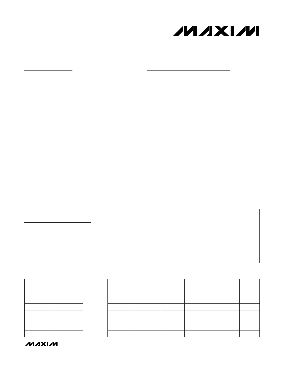
PART
MAX3483ECSA
MAX3483ECPA 0°C to +70°C
0°C to +70°C
TEMP. RANGE PIN-PACKAGE
8 SO
8 Plastic DIP
PART
NUMBER
GUARANTEED
DATA RATE
(Mbps)
SUPPLY
VOLTAGE
(V)
HALF/FULL
DUPLEX
SLEW-RATE
LIMITED
DRIVER/
RECEIVER
ENABLE
SHUTDOWN
CURRENT
(nA)
PIN
COUNT
MAX3483E 0.25 Half Yes Yes 2 8
MAX3485E 12 Half No Yes 2 8
MAX3486E 2.5 Half Yes Yes 2 8
MAX3488E 0.25 Full Yes No — 8
MAX3490E 12 Full No No — 8
MAX3491E 12
3.0 to 3.6
Full No Yes 2 14
Selector Guide
MAX3483EESA
MAX3483EEPA -40°C to +85°C
-40°C to +85°C 8 SO
8 Plastic DIP
MAX3485ECSA
MAX3485ECPA 0°C to +70°C
0°C to +70°C 8 SO
8 Plastic DIP
MAX3485EESA
MAX3485EEPA -40°C to +85°C
-40°C to +85°C 8 SO
8 Plastic DIP
Ordering Information
Ordering Information continued at end of data sheet.
±15kV
ESD
PROTECTION
Yes
Yes
Yes
Yes
Yes
Yes
For free samples & the latest literature: http://www.maxim-ic.com, or phone 1-800-998-8800.
For small orders, phone 1-800-835-8769.
MAX3483E/MAX3485E/MAX3486E/MAX3488E/MAX3490E/MAX3491E
3.3V -Powered, ±15kV ESD-Protected, 12Mbps and
Slew-Rate-Limited True RS-485/RS-422 Transceivers
2 _______________________________________________________________________________________
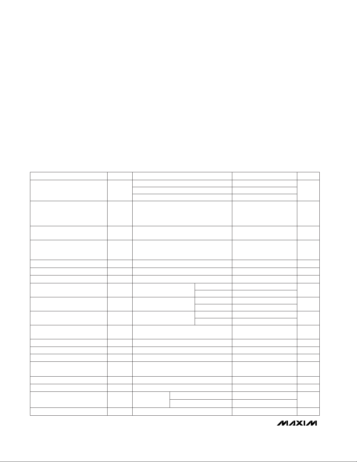
ABSOLUTE MAXIMUM RATINGS
DC ELECTRICAL CHARACTERISTICS
(VCC= +3.3V ±0.3V, TA= T
MIN
to T
MAX
, unless otherwise noted. Typical values are at TA= +25°C.)
Stresses beyond those listed under “Absolute Maximum Ratings” may cause permanent damage to the device. These are stress ratings only, and functional
operation of the device at these or any other conditions beyond those indicated in the operational sections of the specifications is not implied. Exposure to
absolute maximum rating conditions for extended periods may affect device reliability.
Supply Voltage (VCC).............................................................+7V
Control Input Voltage (
RE, DE).................................-0.3V to +7V
Driver Input Voltage (DI)...........................................-0.3V to +7V
Driver Output Voltage (A, B, Y, Z).......................-7.5V to +12.5V
Receiver Input Voltage (A, B)..............................-7.5V to +12.5V
Receiver Output Voltage (RO)....................-0.3V to (V
CC
+ 0.3V)
Continuous Power Dissipation (T
A
= +70°C)
8-Pin SO (derate 5.88mW/°C above +70°C)..................471mW
8-Pin Plastic DIP (derate 9.09mW/°C above +70°C) .....727mW
14-Pin SO (derate 8.33mW/°C above +70°C)................667mW
14-Pin Plastic DIP (derate 10mW/°C above +70°C) ......800mW
Operating Temperature Ranges
MAX34_ _ EC_ _ ...................................................0°C to +70°C
MAX34_ _ EE_ _.................................................-40°C to +85°C
Storage Temperature Range.............................-65°C to +150°C
Lead Temperature (soldering, 10sec).............................+300°C
DE = 0,
V
CC
= 0 or 3.6V
DE = 0, RE = VCC,
V
CC
= 0 or 3.6V, MAX3491E
DE = 0, RE = 0,
V
CC
= 0 or 3.6V, MAX3491E
kΩ12R
IN
Receiver Input Resistance
µA±1I
OZR
Three-State (High-Impedance)
Output Current at Receiver
V0.4V
OL
Receiver Output Low Voltage
VVCC- 0.4V
OH
Receiver Output High Voltage
mV50∆V
TH
Receiver Input Hysteresis
V-0.2 0.2V
TH
Receiver Differential
Threshold Voltage
µA
-1
I
O
Output Leakage (Y, Z)
in Shutdown Mode
1
µA
-20
I
O
Output Leakage (Y, Z)
V0.2∆V
OD
Change in Magnitude of Driver
Differential Output Voltage for
Complementary Output States
(Note 1)
V
1.5
V
OD
2.0
Differential Driver Output
20
mA
-0.8
I
IN2
Input Current (A, B)
1.0
µA±2I
IN1
Logic Input Current
V3V
OC
Driver Common-Mode Output
Voltage
V0.2∆V
OC
Change in Magnitude of
Common-Mode Output Voltage
(Note 1)
V2.0V
IH
Input High Voltage
V0.8V
IL
Input Low Voltage
UNITS
MIN TYP MAX
SYMBOLPARAMETER
RL= 54Ω or 100Ω, Figure 4
-7V ≤ VCM≤ 12V
RL= 54Ω (RS-485), Figure 4
VCC= 3.6V, 0 ≤ V
OUT
≤ V
CC
RL= 100Ω (RS-422), Figure 4
I
OUT
= 2.5mA, VID= 200mV, Figure 6
I
OUT
= -1.5mA, VID= 200mV, Figure 6
VCM= 0
V
OUT
= 12V
VIN= -7V
-7V ≤ VCM≤ 12V
V
OUT
= -7V
VIN= 12V
DE, DI, RE
RL= 54Ω or 100Ω, Figure 4
RL= 54Ω or 100Ω, Figure 4
DE, DI, RE
V
OUT
= 12V
DE, DI, RE
V
OUT
= -7V
CONDITIONS
RL= 60Ω (RS-485), VCC= 3.3V, Figure 5
1.5
mA
1.1 2.2
I
CC
Supply Current
No load,
DI = 0 or V
CC
DE = VCC, RE = 0 or V
CC
DE = 0, RE = 0
0.95 1.9
V3.0 3.6V
CC
Supply Voltage Range
µA0.002 1I
SHDN
Supply Current in Shutdown Mode
DE = 0, RE = VCC, DI = VCCor 0
MAX3483E/MAX3485E/MAX3486E/MAX3488E/MAX3490E/MAX3491E
3.3V -Powered, ±15kV ESD-Protected, 12Mbps and
Slew-Rate-Limited True RS-485/RS-422 Transceivers
_______________________________________________________________________________________ 3
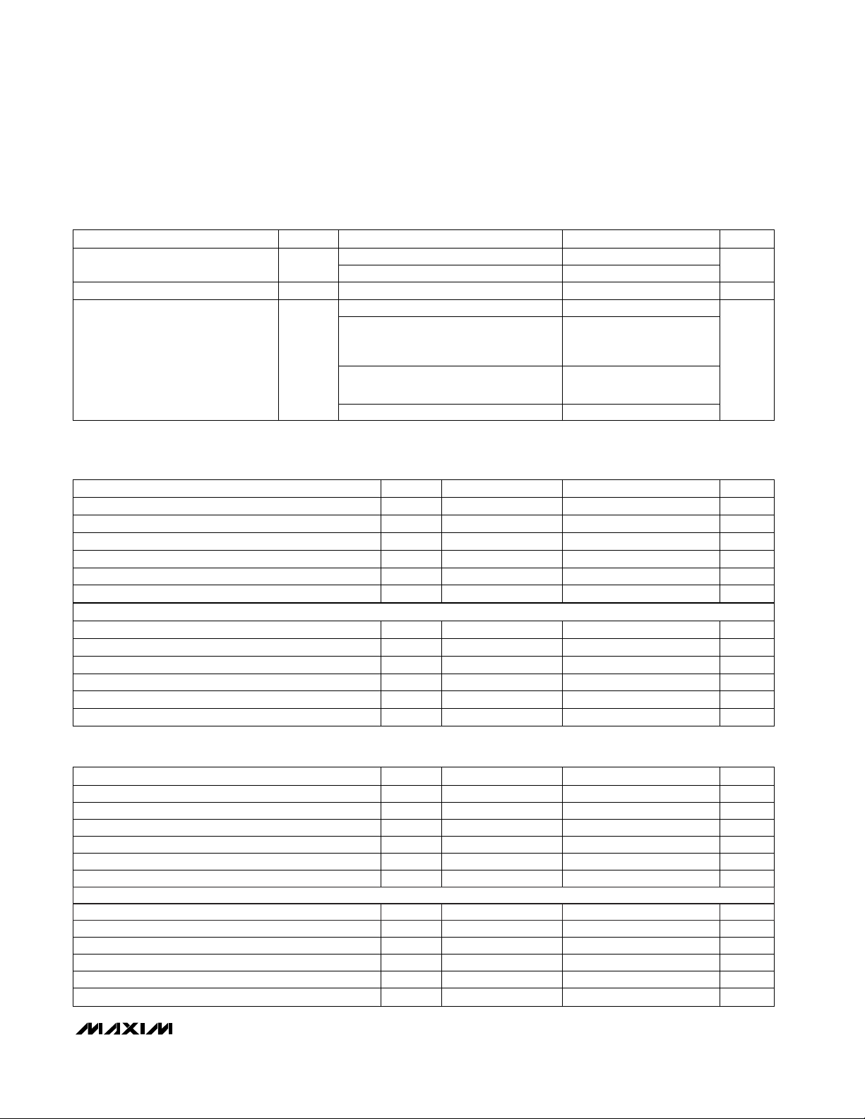
mA
-250
I
OSD
250
Driver Short-Circuit Output Current
mA±8 ±60I
OSR
Receiver Short-Circuit Output Current
UNITSMIN TYP MAXSYMBOLPARAMETER
V
OUT
= -7V
V
OUT
= 12V
0 ≤ VRO≤ V
CC
CONDITIONS
DC ELECTRICAL CHARACTERISTICS (continued)
(VCC= +3.3V ±0.3V, TA= T
MIN
to T
MAX
, unless otherwise noted. Typical values are at TA= +25°C.)
ns72335t
PLH
Driver Propagation Delay, Low-to-High Level
ns31125t
TD
Mbps12 15Maximum Data Rate
Driver Differential Output Transition Time
ns650 900t
PSH
Driver-Output Enable Time from Shutdown to High Level
ns650 900t
PSL
Driver-Output Enable Time from Shutdown to Low Level
ns35 80t
PHZ
Driver-Output Disable Time from High Level
ns72335t
PHL
Driver Propagation Delay, High-to-Low Level
ns-1.4 ±8t
PDS
|
t
PLH
- t
PHL|
Driver Propagation-Delay Skew (Note 2)
ns42 90t
PZL
Driver-Output Enable Time to Low Level
ns42 90t
PZH
Driver-Output Enable Time to High Level
UNITSMIN TYP MAXSYMBOLPARAMETER
RL= 27Ω, Figure 8
RL= 60Ω, Figure 7
RL= 110Ω, Figure 9
RL= 110Ω, Figure 10
RL= 110Ω, Figure 9
RL= 27Ω, Figure 8
RL= 27Ω, Figure 8
RL= 110Ω, Figure 10
RL= 110Ω, Figure 9
CONDITIONS
DRIVER SWITCHING CHARACTERISTICS—MAX3485E/MAX3490E/MAX3491E
(VCC= +3.3V, TA= +25°C.)
ns35 80t
PLZ
Driver-Output Disable Time from Low Level RL= 110Ω, Figure 10
DRIVER SWITCHING CHARACTERISTICS—MAX3486E
(VCC= +3.3V, TA= +25°C.)
ns40 80t
PLZ
Driver-Output Disable Time from Low Level RL= 110Ω, Figure 10
ns20 42 75t
PLH
Driver Propagation Delay, Low-to-High Level
ns15 28 60t
TD
Mbps2.5Maximum Data Rate
Driver Differential Output Transition Time
ns700 1000t
PSH
Driver-Output Enable Time from Shutdown to High Level
ns700 1000t
PSL
Driver-Output Enable Time from Shutdown to Low Level
ns40 80t
PHZ
Driver-Output Disable Time from High Level
ns20 42 75t
PHL
Driver Propagation Delay, High-to-Low Level
ns-6 ±12t
PDS
|
t
PLH
- t
PHL|
Driver Propagation-Delay Skew (Note 2)
ns52 100t
PZH
Driver-Output Enable Time to High Level
UNITSMIN TYP MAXSYMBOLPARAMETER
RL= 27Ω, Figure 8
RL= 60Ω, Figure 7
RL= 110Ω, Figure 9
RL= 110Ω, Figure 10
RL= 110Ω, Figure 9
RL= 27Ω, Figure 8
RL= 27Ω, Figure 8
RL= 110Ω, Figure 9
CONDITIONS
±15IEC 1000-4-2 Air Discharge
±6
IEC 1000-4-2 Contact Discharge
(MAX3490E, MAX3488E)*
±8
IEC 1000-4-2 Contact Discharge
(MAX3483E, MAX3485E,
MAX3486E, MAX3491E)
ns12235t
DD
Driver Differential Output Delay RL= 60Ω, Figure 7
DRIVER-OUTPUT ENABLE/DISABLE TIMES (MAX3485E/MAX3491E only)
ns20 42 70t
DD
Driver Differential Output Delay RL= 60Ω, Figure 7
ESD Protection for Y, Z, A, B
±15Human Body Model
kV
*
MAX3488E and MAX3491E will be compliant to ±8kV per IEC 1000-4-2 Contact Discharge by September 1999.
ns52 100t
PZL
Driver-Output Enable Time to Low Level RL= 110Ω, Figure 10
DRIVER-OUTPUT ENABLE/DISABLE TIMES
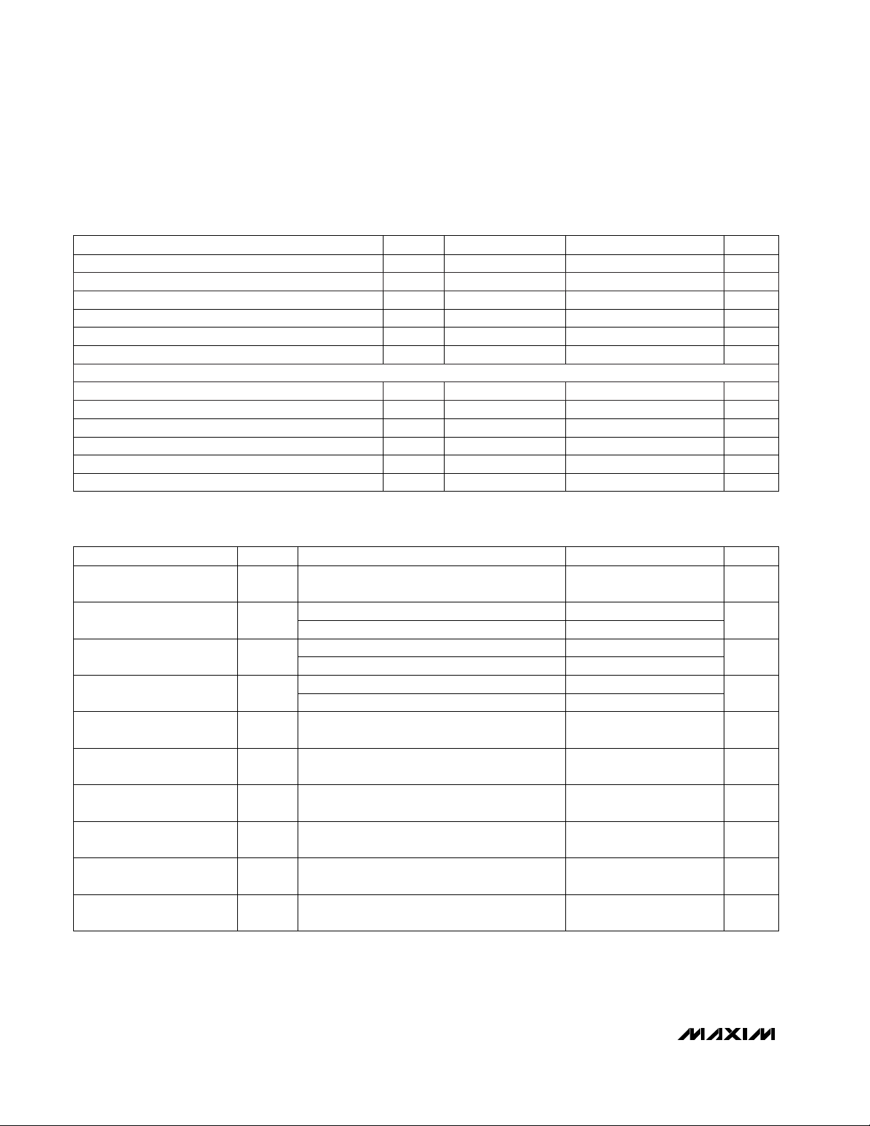
MAX3483E/MAX3485E/MAX3486E/MAX3488E/MAX3490E/MAX3491E
3.3V -Powered, ±15kV ESD-Protected, 12Mbps and
Slew-Rate-Limited True RS-485/RS-422 Transceivers
4 _______________________________________________________________________________________
DRIVER SWITCHING CHARACTERISTICS—MAX3483E/MAX3488E
(VCC= +3.3V, TA= +25°C.)
ns50 80t
PLZ
Driver-Output Disable Time from Low Level RL= 110Ω, Figure 10
ns700 930 1500t
PLH
Driver Propagation Delay, Low-to-High Level
ns400 740 1200t
TD
kbps250Maximum Data Rate
Driver Differential Output Transition Time
µs2.2 3.0t
PSH
Driver-Output Enable Time from Shutdown to High Level
µs1.9 2.7t
PSL
Driver-Output Enable Time from Shutdown to Low Level
ns50 80t
PHZ
Driver-Output Disable Time from High Level
ns700 930 1500t
PHL
Driver Propagation Delay, High-to-Low Level
ns±50t
PDS
|
t
PLH
- t
PHL|
Driver Propagation-Delay Skew (Note 2)
ns600 800t
PZH
Driver-Output Enable Time to High Level
UNITSMIN TYP MAXSYMBOLPARAMETER
RL= 27Ω, Figure 8
RL= 60Ω, Figure 7
RL= 110Ω, Figure 9
RL= 110Ω, Figure 10
RL= 110Ω, Figure 9
RL= 27Ω, Figure 8
RL= 27Ω, Figure 8
RL= 110Ω, Figure 9
CONDITIONS
RECEIVER SWITCHING CHARACTERISTICS
(VCC= +3.3V, TA= +25°C.)
ns25 45t
PRLZ
Receiver-Output Disable
Time from Low Level
CL= 15pF, Figure 12,
MAX3483E/85E/86E/91E only
ns
25 62 90
ns80 190 300t
SHDN
Time to Shutdown
ns720 1400t
PRSH
Receiver-Output Enable Time
from Shutdown to High Level
ns720 1400t
PRSL
Receiver-Output Enable Time
from Shutdown to Low Level
ns25 45t
PRHZ
Receiver-Output Disable
Time from High Level
ns
25 62 90
ns
6±10
ns25 50t
PRZL
Receiver-Output Enable Time
to Low Level
ns25 50t
PRZH
Receiver-Output Enable Time
to High Level
UNITSMIN TYP MAXSYMBOLPARAMETER
VID= 0 to 3.0V, CL= 15pF, Figure 11
MAX3483E/MAX3485E/MAX3486E/MAX3491E
only (Note 3)
CL= 15pF, Figure 12,
MAX3483E/85E/86E/91E only
CL= 15pF, Figure 12,
MAX3483E/85E/86E/91E only
CL= 15pF, Figure 12,
MAX3483E/85E/86E/91E only
VID= 0 to 3.0V, CL= 15pF, Figure 11
VID= 0 to 3.0V, CL= 15pF, Figure 11
CL= 15pF, Figure 12,
MAX3483E/85E/86E/91E only
CL= 15pF, Figure 12,
MAX3483E/85E/86E/91E only
CONDITIONS
25 75 120
t
RPLH
Receiver Propagation Delay,
Low-to-High Level
MAX3483E/MAX3488E
25 75 120
t
RPHL
Receiver Propagation Delay,
High-to-Low Level
MAX3483E/MAX3488E
12 ±20
t
RPDS
|
t
PLH
- t
PHL|
Receiver
Propagation-Delay Skew
MAX3483E/MAX3488E
Note 1: ∆VODand ∆VOCare the changes in VODand VOC, respectively, when the DI input changes state.
Note 2: Measured on
|t
PLH
(Y) - t
PHL
(Y)| and |t
PLH
(Z) - t
PHL
(Z)|.
Note 3: The transceivers are put into shutdown by bringing RE high and DE low. If the inputs are in this state for less than 80ns, the
devices are guaranteed not to enter shutdown. If the inputs are in this state for at least 300ns, the devices are guaranteed
to have entered shutdown. See
Low-Power Shutdown Mode
section.
ns900 1300t
PZL
Driver-Output Enable Time to Low Level RL= 110Ω, Figure 10
ns600 900 1400t
DD
Driver Differential Output Delay RL= 60Ω, Figure 7
DRIVER-OUTPUT ENABLE/DISABLE TIMES (MAX3483E only)
MAX3483E/MAX3485E/MAX3486E/MAX3488E/MAX3490E/MAX3491E
3.3V -Powered, ±15kV ESD-Protected, 12Mbps and
Slew-Rate-Limited True RS-485/RS-422 Transceivers
_______________________________________________________________________________________
5
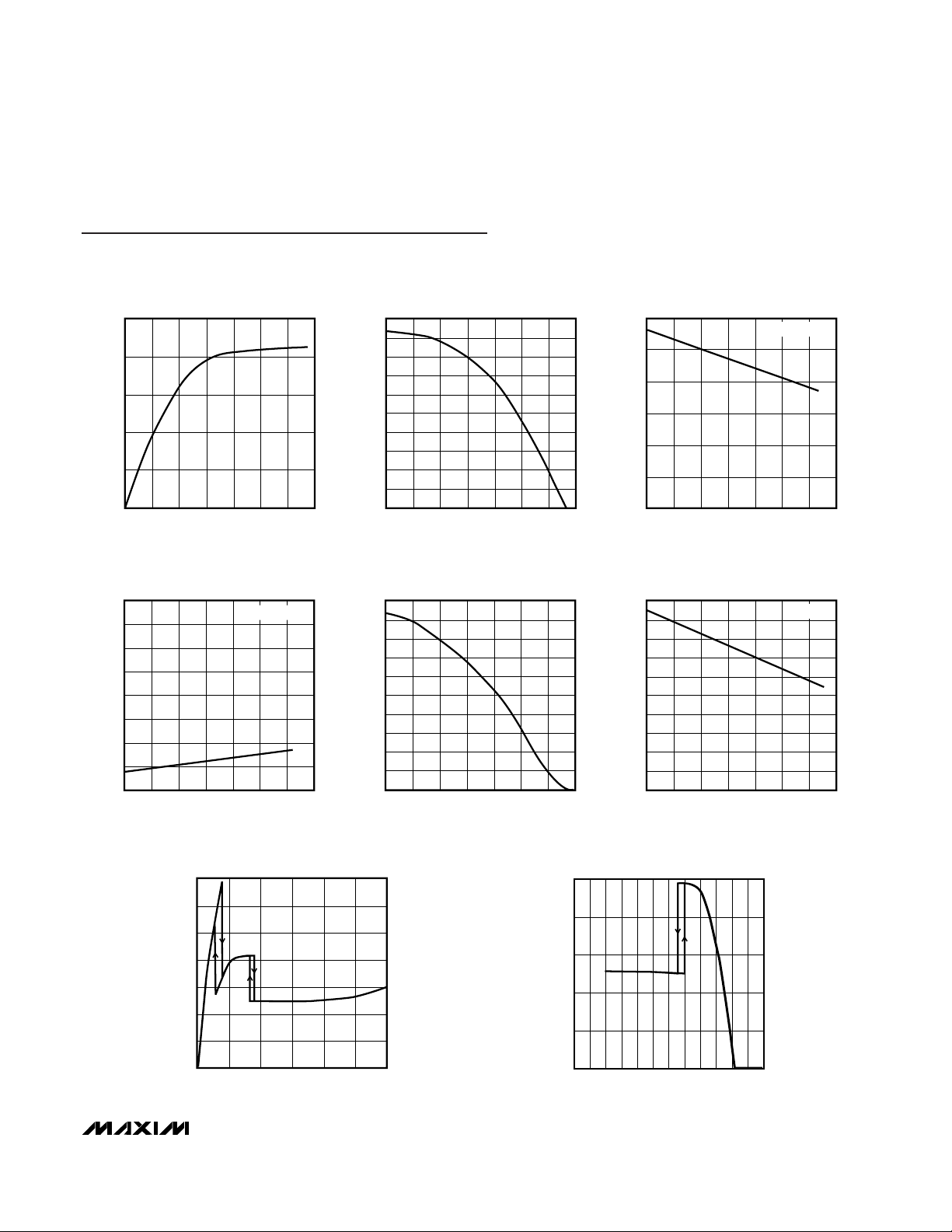
Typical Operating Characteristics
(VCC= +3.3V, TA= +25°C, unless otherwise noted.)
25
20
15
10
5
0
0 0.5 1.0 1.5 2.0 2.5 3.53.0
OUTPUT CURRENT vs.
RECEIVER OUTPUT LOW VOLTAGE
MAX3483E-01
OUTPUT LOW VOLTAGE (V)
OUTPUT CURRENT (mA)
-20
-18
-16
-14
-12
-10
-8
-6
-4
-2
0
0 0.5 1.0 1.5 2.0 2.5 3.53.0
OUTPUT CURRENT vs.
RECEIVER OUTPUT HIGH VOLTAGE
MAX3483E-02
OUTPUT HIGH VOLTAGE (V)
OUTPUT CURRENT (mA)
3.00
3.05
3.10
3.15
3.20
3.25
3.30
-40 -20 0 20 40 60 10080
RECEIVER OUTPUT HIGH VOLTAGE
vs. TEMPERATURE
MAX3483E-03
TEMPERATURE (°C)
OUTPUT HIGH VOLTAGE (V)
IRO = 1.5mA
0
0.1
0.2
0.3
0.4
0.5
0.6
0.7
0.8
-40 -20 0 20 40 60 10080
RECEIVER OUTPUT LOW VOLTAGE
vs. TEMPERATURE
MAX3483E-04
TEMPERATURE (°C)
OUTPUT LOW VOLTAGE (V)
IRO = 2.5mA
25
0
50
75
100
125
150
175
0246 81012
OUTPUT CURRENT vs.
DRIVER OUTPUT LOW VOLTAGE
MAX3483E-07
OUTPUT LOW VOLTAGE (V)
OUTPUT CURRENT (mA)
100
90
80
70
60
50
40
30
20
10
0
0 0.5 1.0 1.5 2.0 2.5 3.53.0
DRIVER OUTPUT CURRENT vs.
DIFFERENTIAL OUTPUT VOLTAGE
MAX3483E-05
DIFFERENTIAL OUTPUT VOLTAGE (V)
OUTPUT CURRENT (mA)
1.6
1.7
1.8
1.9
2.0
2.1
2.2
2.3
2.4
2.6
2.5
-40 -20 0 20 40 60 10080
DRIVER DIFFERENTIAL OUTPUT
VOLTAGE vs. TEMPERATURE
MAX3483E-06
TEMPERATURE (°C)
DIFFERENTIAL OUTPUT VOLTAGE (V)
R = 54Ω
0
-100
-80
-60
-40
-20
543210
-7 -6 -3-4-5 -2 -1
OUTPUT CURRENT vs.
DRIVER OUTPUT HIGH VOLTAGE
MAX3483E-08
OUTPUT HIGH VOLTAGE (V)
OUTPUT CURRENT (mA)

MAX3483E/MAX3485E/MAX3486E/MAX3488E/MAX3490E/MAX3491E
3.3V -Powered, ±15kV ESD-Protected, 12Mbps and
Slew-Rate-Limited True RS-485/RS-422 Transceivers
6 _______________________________________________________________________________________
0.8
0.7
0.9
1.0
1.1
1.2
-40 -20 0 20 40 60 10080
SUPPLY CURRENT
vs. TEMPERATURE
MAX3483E-09
TEMPERATURE (°C)
SUPPLY CURRENT (mA)
X = DON’T CARE
DE = VCC, RE = X
DE = 0, RE = 0
Typical Operating Characteristics (continued)
(VCC= +3.3V, TA= +25°C, unless otherwise noted.)
0
10
20
30
40
50
60
70
80
100
90
-40 -20 0 20 40 60 10080
SHUTDOWN CURRENT
vs. TEMPERATURE
MAX3483E-10
TEMPERATURE (°C)
SHUTDOWN CURRENT (nA)
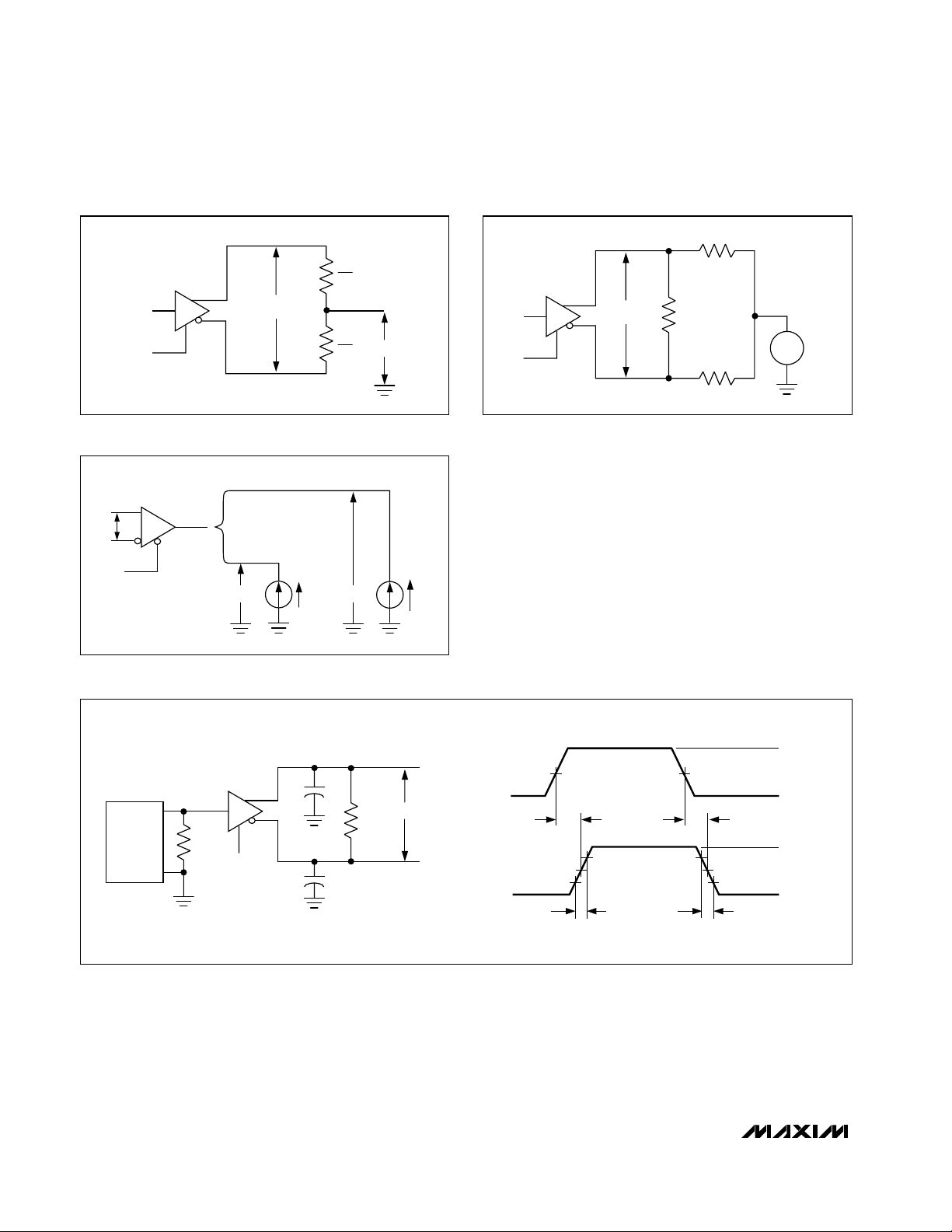
Pin Description
—
—
3
4
5
6
—
8
—
7
1
—
MAX3483E
MAX3485E
MAX3486E
21
2
3
4
5
—
—
6
—
7
—
8
—
2
Receiver Output. If A > B by 200mV, RO will be high; if A < B by 200mV,
RO will be low.
3
Receiver Output Enable. RO is enabled when RE is low; RO is high impedance when RE is high. If RE is high and DE is low, the device will enter a
low-power shutdown mode.
4
Driver Output Enable. The driver outputs are enabled by bringing DE high.
They are high impedance when DE is low. If RE is high and DE is low, the
device will enter a low-power shutdown mode. If the driver outputs are
enabled, the parts function as line drivers. While they are high impedance,
they function as line receivers if RE is low.
5
Driver Input. A low on DI forces output Y low and output Z high. Similarly, a
high on DI forces output Y high and output Z low.
6, 7 Ground
9 Noninverting Driver Output
10 Inverting Driver Output
— Noninverting Receiver Input and Noninverting Driver Output
12 Noninverting Receiver Input
RO
RE
DE
DI
GND
Y
Z
A
A
— B Inverting Receiver Input and Inverting Driver Output
11 B Inverting Receiver Input
13, 14 V
CC
Positive Supply: 3.0V ≤ VCC≤ 3.6V. Do not operate device with VCC> 3.6V.
1, 8 N.C. No Connection. Not internally connected.
MAX3488E
MAX3490E
PIN
FUNCTION
MAX3491E
FUNCTION
NAME
NAME

MAX3483E/MAX3485E/MAX3486E/MAX3488E/MAX3490E/MAX3491E
3.3V -Powered, ±15kV ESD-Protected, 12Mbps and
Slew-Rate-Limited True RS-485/RS-422 Transceivers
_______________________________________________________________________________________ 7
MAX3483E
MAX3485E
MAX3486E
TOP VIEW
NOTE: PIN LABELS Y AND Z ON TIMING, TEST, AND WAVEFORM DIAGRAMS REFER TO PINS A AND B WHEN DE IS HIGH.
1
2
3
4
8
5
V
CC
GND
DI
DE
RE
RO
R
D
Rt
Rt
7
6
D
R
DE
RE
DI
RO
A
B
1
2
3
4
8
7
6
5
V
CC
B
A
GND
DI
DE
RE
RO
SO/DIP
R
D
B
A
Figure 2. MAX3488E/MAX3490E Pin Configuration and Typical Operating Circuit
Figure 3. MAX3491E Pin Configuration and Typical Operating Circuit
Figure 1. MAX3483E/MAX3485E/MAX3486E Pin Configuration and Typical Operating Circuit
V
TOP VIEW
V
GND
V
CC
1
MAX3488E
MAX3490E
Y
3
A
1
CC
RO
DI
R
2
3
4
D
8
B
7
6
Z
Y
5
DI
RO
DR
2
5
6
Z
8
A
R
Rt
7
B
Rt
SO/DIP
4
GND
CC
D
GND
RO
DI
TOP VIEW
14
V
CC
V
13
CC
12
A
B
11
10
Z
Y
9
8
N.C.
N.C.
5
DI
2
RO
1, 8
N.C.
GND
GND
1
RO
2
3
RE
DE
4
5
DI
6
7
R
D
SO/DIP
DE V
CC
13, 144
9
Y
D
3 6, 7
10
Z
12
A
RD
11
B
RE GND
MAX3491E
Rt
VCCRE
Rt
R
GND DE
RO
DI
MAX3483E/MAX3485E/MAX3486E/MAX3488E/MAX3490E/MAX3491E
3.3V -Powered, ±15kV ESD-Protected, 12Mbps and
Slew-Rate-Limited True RS-485/RS-422 Transceivers
8 _______________________________________________________________________________________
V
CC
D
V
OD
V
OC
2
R
L
2
R
L
Figure 4. Driver VODand V
OC
Figure 7. Driver Differential Output Delay and Transition Times
Figure 6. Receiver V
OH
and V
OL
Figure 5. Driver VODwith Varying Common-Mode Voltage
375Ω
VCM =
V
D
V
CC
OD
R
L
375Ω
-7V to +12V
V
ID
0
GENERATOR
(NOTE 4)
R
50Ω
V
OL
C
L
D
V
CC
C
L
V
OH
I
OL
(+)
R
L
60Ω
C
= 15pF (NOTE 5)
L
I
OH
(-)
3V
IN
OUT
=
OUT
1.5V
t
DD
90%
50%
10%
t
TD
1.5V
90%
0
t
DD
≈ 2.0V
50%
10%
t
TD
≈ -2.0V

MAX3483E/MAX3485E/MAX3486E/MAX3488E/MAX3490E/MAX3491E
3.3V -Powered, ±15kV ESD-Protected, 12Mbps and
Slew-Rate-Limited True RS-485/RS-422 Transceivers
_______________________________________________________________________________________ 9
V
CC
V
OM
3V
0V
V
OH
V
OM
V
OM
V
OM
V
OM
V
OL
V
OH
V
OL
50Ω
R
L
= 27Ω
CL = 15pF
(NOTE 5)
GENERATOR
(NOTE 4)
D
t
PLH
1.5V
Y
OUT
Z
OUT
OUT
S1
IN
1.5V
≈ 1.5V
t
PHL
t
PHL
t
PLH
VOH + V
OL
2
V
OM
=
Figure 8. Driver Propagation Times
Figure 9. Driver Enable and Disable Times (t
PZH
, t
PSH
, t
PHZ
)
Figure 10. Driver Enable and Disable Times (t
PZL
, t
PSL
, t
PLZ
)
S1
D0 OR 3V
C
= 50pF
L
GENERATOR
(NOTE 4)
(NOTE 5)
50Ω
S1
0 OR 3V
GENERATOR
(NOTE 4)
D
= 50pF
C
L
(NOTE 5)
50Ω
V
OM
=
VOH + V
2
V
CC
OL
≈ 1.5V
RL = 110Ω
= 110Ω
R
L
OUT
OUT
3V
IN
OUT
IN
OUT
t
PSL
1.5V
t
PZH
1.5V
V
OM
V
OM
1.5V
0
t
PHZ
V
OH
0.25V
0
3V
1.5V
0
t
PLZ
V
0.25V
CC
V
OL
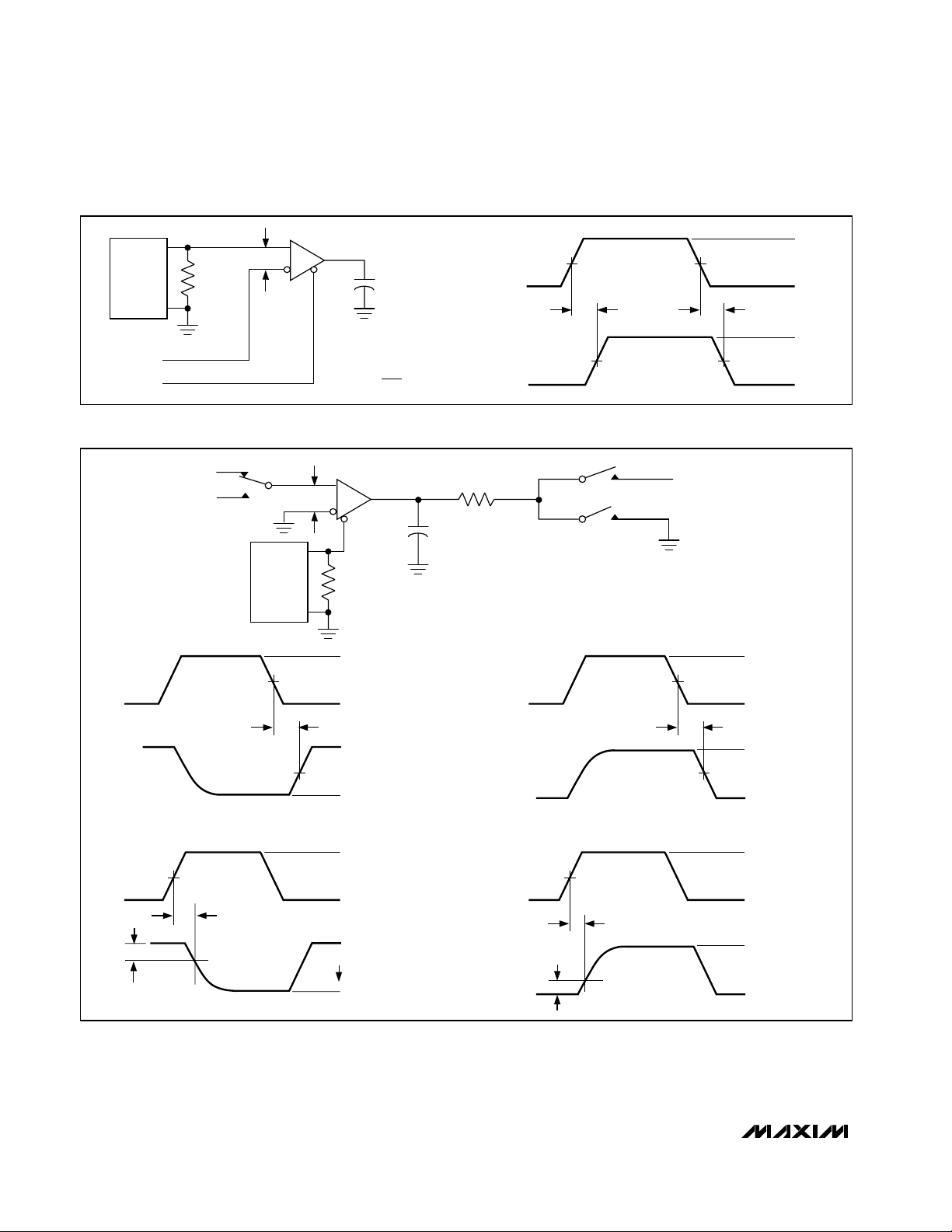
MAX3483E/MAX3485E/MAX3486E/MAX3488E/MAX3490E/MAX3491E
3.3V -Powered, ±15kV ESD-Protected, 12Mbps and
Slew-Rate-Limited True RS-485/RS-422 Transceivers
10 ______________________________________________________________________________________
V
ID
50Ω
C
L
= 15pF
(NOTE 5)
GENERATOR
(NOTE 4)
R
OUT
t
RPLH
1.5V
OUT
1.5V
0
IN
1.5V
3.0V
0
t
RPHL
V
CC
V
OM
V
OM
0
V
CC
2
V
OM
=
Figure 11. Receiver Propagation Delay
Figure 12. Receiver Enable and Disable Times
Note 4: The input pulse is supplied by a generator with the following characteristics: f = 250kHz, 50% duty cycle, tr≤ 6.0ns, ZO= 50Ω.
Note 5: C
L
includes probe and stray capacitance.
OUT
OUT
0.25V
S1
V
CC
S2
3V
0
V
V
3V
0
V
V
S1 CLOSED
S2 OPEN
S3 = -1.5V
CC
OL
S1 CLOSED
S2 OPEN
S3 = -1.5V
CC
OL
1.5V
t
PRLZ
t
PRZL
tPRSL
1.5V
1.5V
t
PRZH
tPRSH
t
PRHZ
S3
GENERATOR
(NOTE 4)
1.5V
1.5V
1k
V
ID
R
CL
(NOTE 5)
50Ω
3V
0
V
0
3V
0
V
0
S1 OPEN
S2 CLOSED
S3 = 1.5V
OH
S1 OPEN
S2 CLOSED
S3 = 1.5V
OH
IN
OUT
IN
OUT
1.5V
-1.5V
IN
IN
0.25V
1.5V
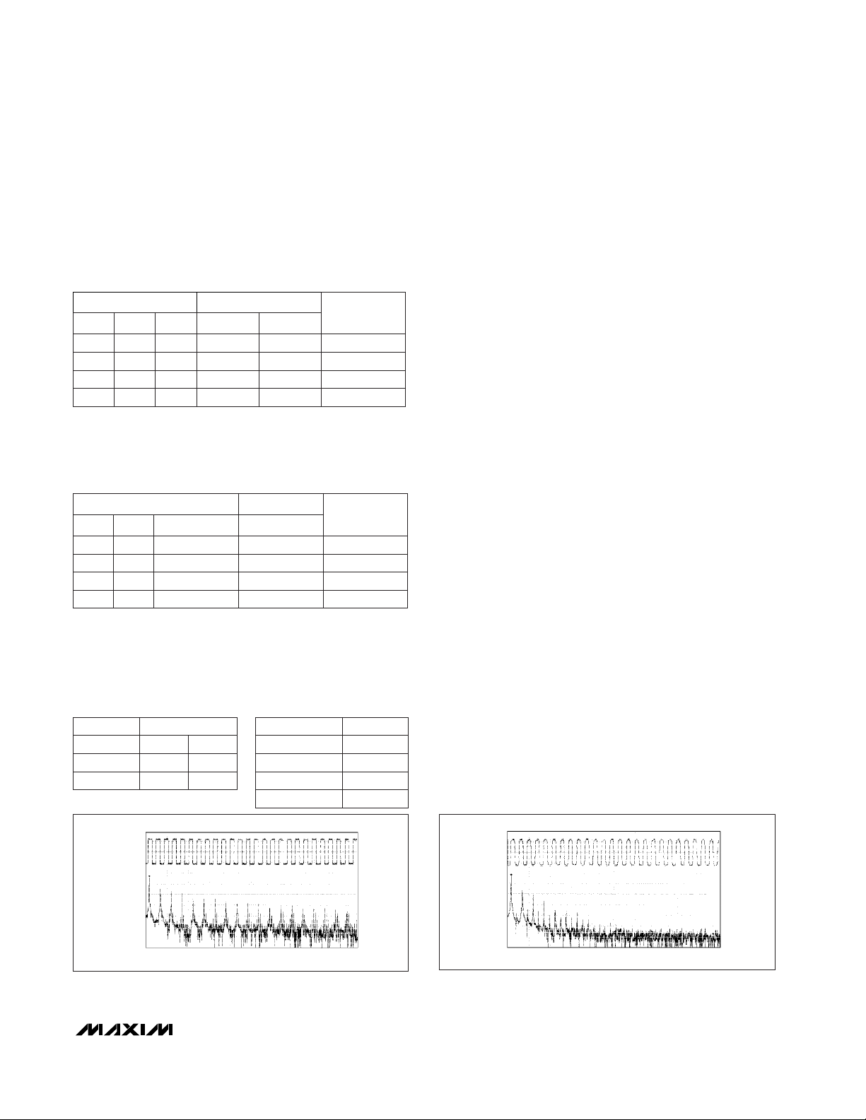
_____________________Function Tables
Devices with Receiver/Driver Enable
(MAX3483E/MAX3485E/MAX3486E/MAX3491E)
Table 1. Transmitting
* B and A outputs are Z and Y, respectively, for full-duplex part
(MAX3491E).
X = Don’t care; High-Z = High impedance
Table 2. Receiving
* DE is a “don’t care” (x) for the full-duplex part (MAX3491E).
X = Don’t care; High-Z = High impedance
Devices without Receiver/Driver Enable
(MAX3488E/MAX3490E)
Table 3. Transmitting Table 4. Receiving
___________Applications Information
The MAX3483E/MAX3485E/MAX3486E/MAX3488E/
MAX3490E/MAX3491E are low-power transceivers for
RS-485 and RS-422 communications. The MAX3483E
and MAX3488E can transmit and receive at data rates
up to 250kbps, the MAX3486E at up to 2.5Mbps, and the
MAX3485E/MAX3490E/MAX3491E at up to 12Mbps. The
MAX3488E/MAX3490E/MAX3491E are full-duplex transceivers, while the MAX3483E/MAX3485E/MAX3486E are
half-duplex. Driver Enable (DE) and Receiver Enable
(RE) pins are included on the MAX3483E/MAX3485E/
MAX3486E/MAX3491E. When disabled, the driver and
receiver outputs are high impedance.
Reduced EMI and Reflections
(MAX3483E/MAX3486E/MAX3488E)
The MAX3483E/MAX3488E are slew-rate limited, minimizing EMI and reducing reflections caused by improperly terminated cables. Figure 13 shows the driver
output waveform of a MAX3485E/MAX3490E/MAX3491E
transmitting a 125kHz signal, as well as the Fourier
analysis of that waveform. High-frequency harmonics
with large amplitudes are evident. Figure 14 shows the
same information, but for the slew-rate-limited
MAX3483E/MAX3488E transmitting the same signal. The
high-frequency harmonics have much lower amplitudes,
and the potential for EMI is significantly reduced.
Low-Power Shutdown Mode
(MAX3483E/MAX3485E/MAX3486E/MAX3491E)
A low-power shutdown mode is initiated by bringing both
RE high and DE low. The devices will not shut down
unless both the driver and receiver are disabled (high
impedance). In shutdown, the devices typically draw
only 2nA of supply current.
For these devices, the t
PSH
and t
PSL
enable times
assume the part was in the low-power shutdown mode;
the t
PZH
and t
PZL
enable times assume the receiver or
driver was disabled, but the part was not shut down.
MAX3483E/MAX3485E/MAX3486E/MAX3488E/MAX3490E/MAX3491E
3.3V -Powered, ±15kV ESD-Protected, 12Mbps and
Slew-Rate-Limited True RS-485/RS-422 Transceivers
______________________________________________________________________________________ 11
INPUTS OUTPUTS
RE
DE DI B* A*
MODE
X 1 1 0 1 Normal
X 1 0 1 0 Normal
0 0 X High-Z High-Z Normal
1 0 X High-Z High-Z Shutdown
INPUTS
RE
DE A, B RO
MODE
0 0* ≥ +0.2V 1 Normal
0 0* ≤ -0.2V 0 Normal
0 0* Inputs Open 1 Normal
1 0 X High-Z Shutdown
OUTPUTS
INPUTS OUTPUT
A, B RO
≥+0.2V 1
≤-0.2V 0
Inputs Open 1
INPUT OUTPUTS
DI Z Y
1 0 1
0 1 0
Figure 13. Driver Output Waveform and FFT Plot of MAX3485E/
MAX3490E/MAX3491E Transmitting a 125kHz Signal
Figure 14. Driver Output Waveform and FFT Plot of
MAX3483E/ MAX3488E Transmitting a 125kHz Signal
10dB/div
5MHz500kHz/div0
10dB/div
5MHz500kHz/div0

MAX3483E/MAX3485E/MAX3486E/MAX3488E/MAX3490E/MAX3491E
3.3V -Powered, ±15kV ESD-Protected, 12Mbps and
Slew-Rate-Limited True RS-485/RS-422 Transceivers
12 ______________________________________________________________________________________
B
1V/div
A
1V/div
RO
2V/div
20ns/div
Figure 15. MAX3485E/MAX3490E/MAX3491E Driver Propagation
Delay
Figure 17. MAX3483E/MAX3488E Driver Propagation Delay
Figure 16. MAX3485E/MAX3490E/MAX3491E Receiver
Propagation Delay Driven by External RS-485 Device
Figure 18. MAX3483E/MAX3488E Receiver Propagation Delay
Figure 19. MAX3483E/MAX3488E System Differential Voltage at
125kHz Driving 4000 Feet of Cable
Figure 20. MAX3485E/MAX3490E/MAX3491E System Differential
Voltage at 125kHz Driving 4000 Feet of Cable
DI
2V/div
Z
1V/div
Y
1V/div
20ns/div
DI
2V/div
Z
1V/div
Y
1V/div
1µs/div
DI
5V/div
- V
V
Y
Z
2V/div
B
1V/div
A
1V/div
RO
2V/div
1µs/div
DI
5V/div
- V
V
Y
Z
2V/div
RO
5V/div
2µs/div
RO
5V/div
2µs/div

MAX3483E/MAX3485E/MAX3486E/MAX3488E/MAX3490E/MAX3491E
3.3V -Powered, ±15kV ESD-Protected, 12Mbps and
Slew-Rate-Limited True RS-485/RS-422 Transceivers
______________________________________________________________________________________ 13
Driver-Output Protection
Excessive output current and power dissipation caused
by faults or by bus contention are prevented by two
mechanisms. A foldback current limit on the output stage
provides immediate protection against short circuits over
the whole common-mode voltage range (see
Typical
Operating Characteristics
). In addition, a thermal shutdown circuit forces the driver outputs into a high-impedance state if the die temperature rises excessively.
Propagation Delay
Figures 15–18 show the typical propagation delays. Skew
time is simply the difference between the low-to-high and
high-to-low propagation delay. Small driver/receiver
skew times help maintain a symmetrical mark-space
ratio (50% duty cycle).
The receiver skew time, |t
PRLH
- t
PRHL|
, is under 10ns
(20ns for the MAX3483E/MAX3488E). The driver skew
times are 8ns for the MAX3485E/MAX3490E/MAX3491E,
12ns for the MAX3486E, and typically under 50ns for the
MAX3483E/MAX3488E.
Line Length vs. Data Rate
The RS-485/RS-422 standard covers line lengths up to
4000 feet. For line lengths greater than 4000 feet, see
Figure 21 for an example of a line repeater.
Figures 19 and 20 show the system differential voltage
for parts driving 4000 feet of 26AWG twisted-pair wire
at 125kHz into 120Ω loads.
For faster data rate transmission, please consult the factory.
±15kV ESD Protection
As with all Maxim devices, ESD-protection structures are
incorporated on all pins to protect against electrostatic
discharges encountered during handling and assembly.
The driver outputs and receiver inputs of the MAX3483E
family of devices have extra protection against static
electricity. Maxim’s engineers have developed state-ofthe-art structures to protect these pins against ESD of
±15kV without damage. The ESD structures withstand
high ESD in all states: normal operation, shutdown, and
powered down. After an ESD event, Maxim’s E versions
keep working without latchup or damage.
ESD protection can be tested in various ways; the
transmitter outputs and receiver inputs of this product
family are characterized for protection to the following
limits:
1) ±15kV using the Human Body Model
2) ±8kV using the Contact-Discharge method specified
in IEC 1000-4-2
3) ±15kV using IEC 1000-4-2’s Air-Gap method.
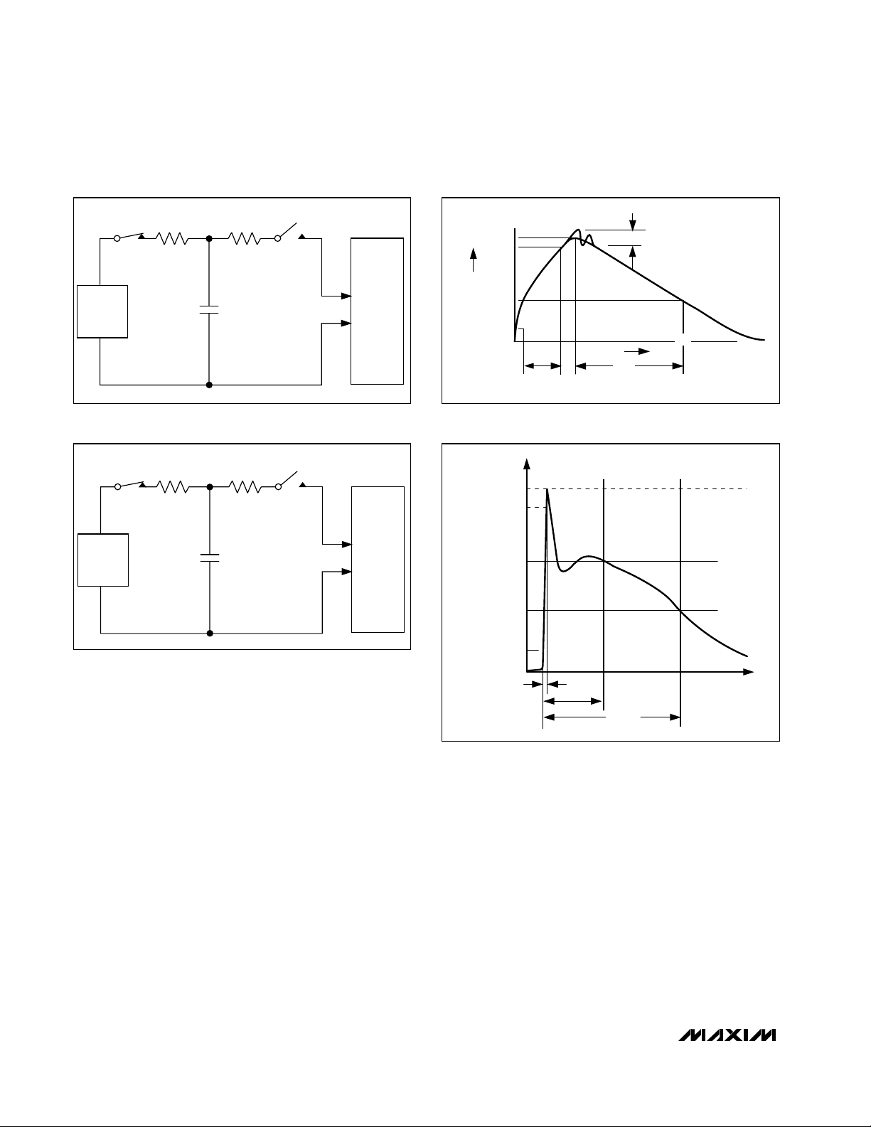
ESD Test Conditions
ESD performance depends on a variety of conditions.
Contact Maxim for a reliability report that documents
test setup, test methodology, and test results.
Human Body Model
Figure 22a shows the Human Body Model and Figure
22b shows the current waveform it generates when discharged into a low impedance. This model consists of
a 100pF capacitor charged to the ESD voltage of interest, which is then discharged into the test device
through a 1.5kΩ resistor.
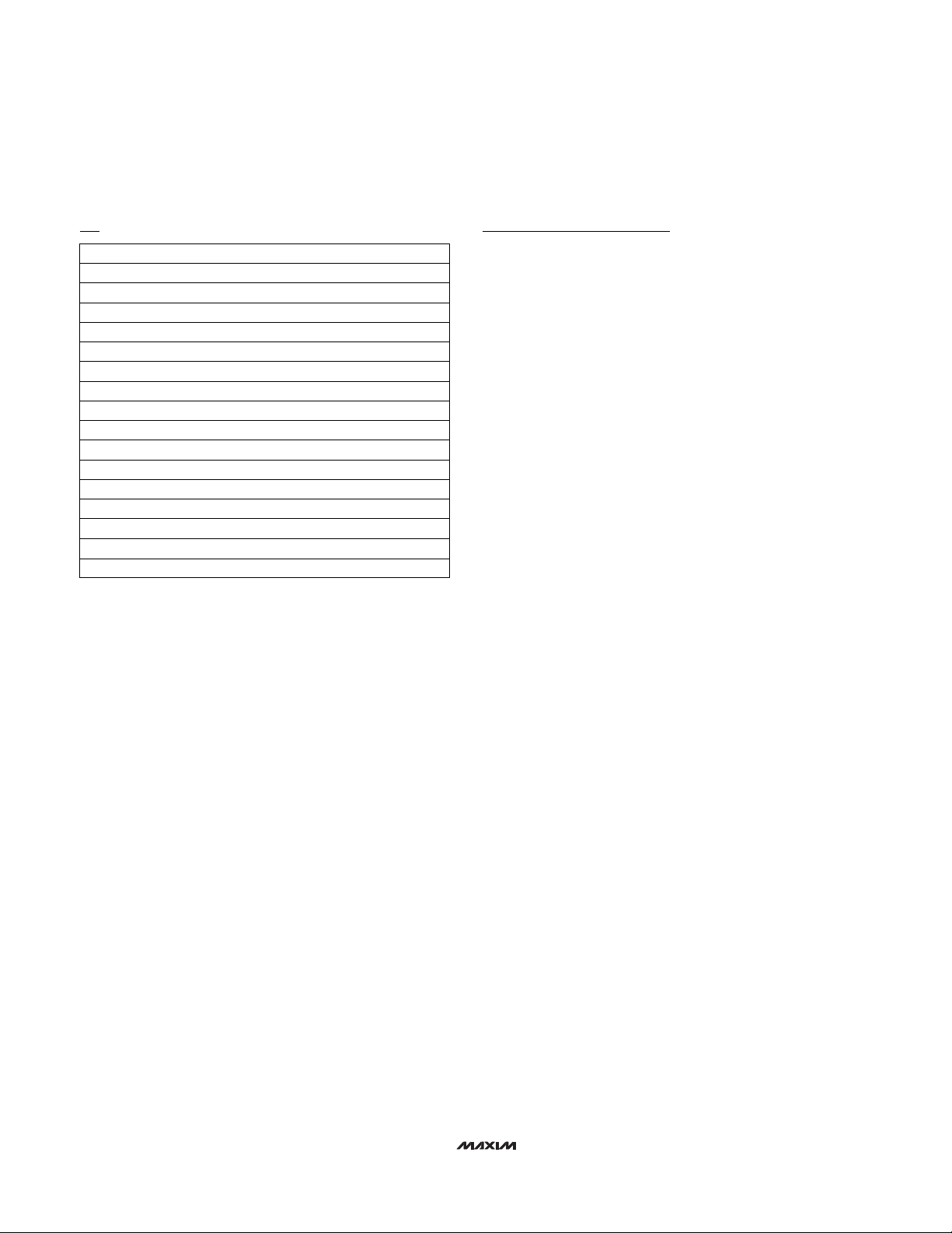
IEC 1000-4-2
The IEC 1000-4-2 standard covers ESD testing and
performance of finished equipment; it does not specifically refer to integrated circuits. The MAX3483E family
of devices helps you design equipment that meets
Level 4 (the highest level) of IEC 1000-4-2, without the
need for additional ESD-protection components.
The major difference between tests done using the
Human Body Model and IEC 1000-4-2 is higher peak
current in IEC 1000-4-2, because series resistance is
lower in the IEC 1000-4-2 model. Hence, the ESD withstand voltage measured to IEC 1000-4-2 is generally
lower than that measured using the Human Body
Model. Figure 23a shows the IEC 1000-4-2 model, and
Figure 23b shows the current waveform for the ±8kV
IEC 1000-4-2, Level 4 ESD contact-discharge test.
120Ω
120Ω
DATA IN
DATA OUT
R
D
RO
RE
DE
DI
A
B
Z
Y
MAX3488E
MAX3490E
MAX3491E
NOTE: RE AND DE ON MAX3491E ONLY.
Figure 21. Line Repeater for MAX3488E/MAX3490E/MAX3491E
MAX3483E/MAX3485E/MAX3486E/MAX3488E/MAX3490E/MAX3491E
The air-gap test involves approaching the device with a
charged probe. The contact-discharge method connects
the probe to the device before the probe is energized.
Machine Model
The Machine Model for ESD tests all pins using a
200pF storage capacitor and zero discharge resistance. Its objective is to emulate the stress caused
when I/O pins are contacted by handling equipment
during test and assembly. Of course, all pins require
this protection, not just RS-485 inputs and outputs.
Typical Applications
The MAX3483E/MAX3485E/MAX3486E/MAX3488E/
MAX3490E/MAX3491E transceivers are designed for
bidirectional data communications on multipoint bus
transmission lines. Figures 24 and 25 show typical network applications circuits. These parts can also be
used as line repeaters, with cable lengths longer than
4000 feet, as shown in Figure 21.
To minimize reflections, the line should be terminated at
both ends in its characteristic impedance, and stub
lengths off the main line should be kept as short as
possible. The slew-rate-limited MAX3483E/MAX3488E
and the partially slew-rate-limited MAX3486E are more
tolerant of imperfect termination.
3.3V -Powered, ±15kV ESD-Protected, 12Mbps and
Slew-Rate-Limited True RS-485/RS-422 Transceivers
14 ______________________________________________________________________________________
CHARGE-CURRENT
LIMIT RESISTOR
DISCHARGE
RESISTANCE
STORAGE
CAPACITOR
C
s
100pF
R
C
1M
R
D
1500Ω
HIGH-
VOLTAGE
DC
SOURCE
DEVICE
UNDER
TEST
Figure 22a. Human Body ESD Test Model
IP 100%
90%
36.8%
t
RL
TIME
t
DL
CURRENT WAVEFORM
PEAK-TO-PEAK RINGING
(NOT DRAWN TO SCALE)
I
r
10%
0
0
AMPERES
Figure 22b. Human Body Current Waveform
CHARGE-CURRENT
LIMIT RESISTOR
DISCHARGE
RESISTANCE
STORAGE
CAPACITOR
C
s
150pF
R
C
50M to 100M
R
D
330Ω
HIGH-
VOLTAGE
DC
SOURCE
DEVICE
UNDER
TEST
Figure 23a. IEC 1000-4-2 ESD Test Model
tr = 0.7ns to 1ns
30ns
60ns
t
100%
90%
10%
I
PEAK
I
Figure 23b. IEC 1000-4-2 ESD Generator Current Waveform

MAX3483E/MAX3485E/MAX3486E/MAX3488E/MAX3490E/MAX3491E
3.3V -Powered, ±15kV ESD-Protected, 12Mbps and
Slew-Rate-Limited True RS-485/RS-422 Transceivers
______________________________________________________________________________________ 15
120Ω
120Ω
R
D
RO
RE
DE
DI
A
B
Y
120Ω
120Ω
DI
DI DIRO RO
RO
DE DE
DE
RE
RE
RE
Z
Z
Z
Z
Y
Y
Y
AA
A
BB
B
D
D
D
R
R
R
MAX3488E
MAX3490E
MAX3491E
NOTE: RE AND DE ON MAX3491E ONLY.
Figure 25. MAX3488E/MAX3490E/MAX3491E Full-Duplex RS-485 Network
DI RO DE
RE
A
B
RE
RERE
RO
RO
RO
DI
DI
DI
DE
DE
DE
D
D
D
R
R
R
B
B
B
A
A
A
120Ω
120Ω
D
R
MAX3483E
MAX3485E
MAX3486E
Figure 24. MAX3483E/MAX3485E/MAX3486E Typical RS-485 Network
MAX3483E/MAX3485E/MAX3486E/MAX3488E/MAX3490E/MAX3491E
3.3V -Powered, ±15kV ESD-Protected, 12Mbps and
Slew-Rate-Limited True RS-485/RS-422 Transceivers
TRANSISTOR COUNT: 761
Chip InformationOrdering Information (continued)
PART
MAX3486ECSA
MAX3486ECPA 0°C to +70°C
0°C to +70°C
TEMP. RANGE PIN-PACKAGE
8 SO
8 Plastic DIP
MAX3486EESA
MAX3486EEPA -40°C to +85°C
-40°C to +85°C 8 SO
8 Plastic DIP
MAX3488ECSA
MAX3488ECPA 0°C to +70°C
0°C to +70°C 8 SO
8 Plastic DIP
MAX3488EESA
MAX3488EEPA -40°C to +85°C
-40°C to +85°C 8 SO
8 Plastic DIP
MAX3490ECSA
MAX3490ECPA 0°C to +70°C
0°C to +70°C 8 SO
8 Plastic DIP
MAX3490EESA
MAX3490EEPA -40°C to +85°C
-40°C to +85°C 8 SO
8 Plastic DIP
MAX3491ECSD
MAX3491ECPD 0°C to +70°C
0°C to +70°C 14 SO
14 Plastic DIP
MAX3491EESD
MAX3491EEPD -40°C to +85°C
-40°C to +85°C 14 SO
14 Plastic DIP
Maxim cannot assume responsibility for use of any circuitry other than circuitry entirely embodied in a Maxim product. No circuit patent licenses are
implied. Maxim reserves the right to change the circuitry and specifications without notice at any time.
16
____________________Maxim Integrated Products, 120 San Gabriel Drive, Sunnyvale, CA 94086 408-737-7600
© 1999 Maxim Integrated Products Printed USA is a registered trademark of Maxim Integrated Products.
 Loading...