

19-0333; Rev 0; 12/94
3.3V-Powered, 10Mbps and Slew-Rate-Limited
True RS-485/RS-422 Transceivers
_______________General Description
The MAX3483, MAX3485, MAX3486, MAX3488,
MAX3490, and MAX3491 are 3.3V, low-power transceivers for RS-485 and RS-422 communication. Each
part contains one driver and one receiver. The
MAX3483 and MAX3488 feature slew-rate-limited drivers that minimize EMI and reduce reflections caused
by improperly terminated cables, allowing error-free
data transmission at data rates up to 250kbps. The partially slew-rate-limited MAX3486 transmits up to
2.5Mbps. The MAX3485, MAX3490, and MAX3491
transmit at up to 10Mbps.
Drivers are short-circuit current limited and are protected against excessive power dissipation by thermal
shutdown circuitry that places the driver outputs into a
high-impedance state. The receiver input has a fail-safe
feature that guarantees a logic-high output if both
inputs are open circuit.
The MAX3488, MAX3490, and MAX3491 feature fullduplex communication, while the MAX3483, MAX3485,
and MAX3486 are designed for half-duplex communication.
________________________Applications
Low-Power RS-485/RS-422 Transceivers
Telecommunications
Transceivers for EMI-Sensitive Applications
Industrial-Control Local Area Networks
____________________________Features
♦ Operate from a Single 3.3V Supply—
No Charge Pump!
♦ Interoperable with +5V Logic
♦ 8ns Max Skew (MAX3485/MAX3490/MAX3491)
♦ Slew-Rate Limited for Errorless Data Transmission
(MAX3483/MAX3488)
♦ 2nA Low-Current Shutdown Mode
(MAX3483/MAX3485/MAX3486/MAX3491)
♦ -7V to +12V Common-Mode Input Voltage Range
♦ Allows up to 32 Transceivers on the Bus
♦ Full-Duplex and Half-Duplex Versions Available
♦ Industry Standard 75176 Pinout
(MAX3483/MAX3485/MAX3486)
♦ Current-Limiting and Thermal Shutdown for
Driver Overload Protection
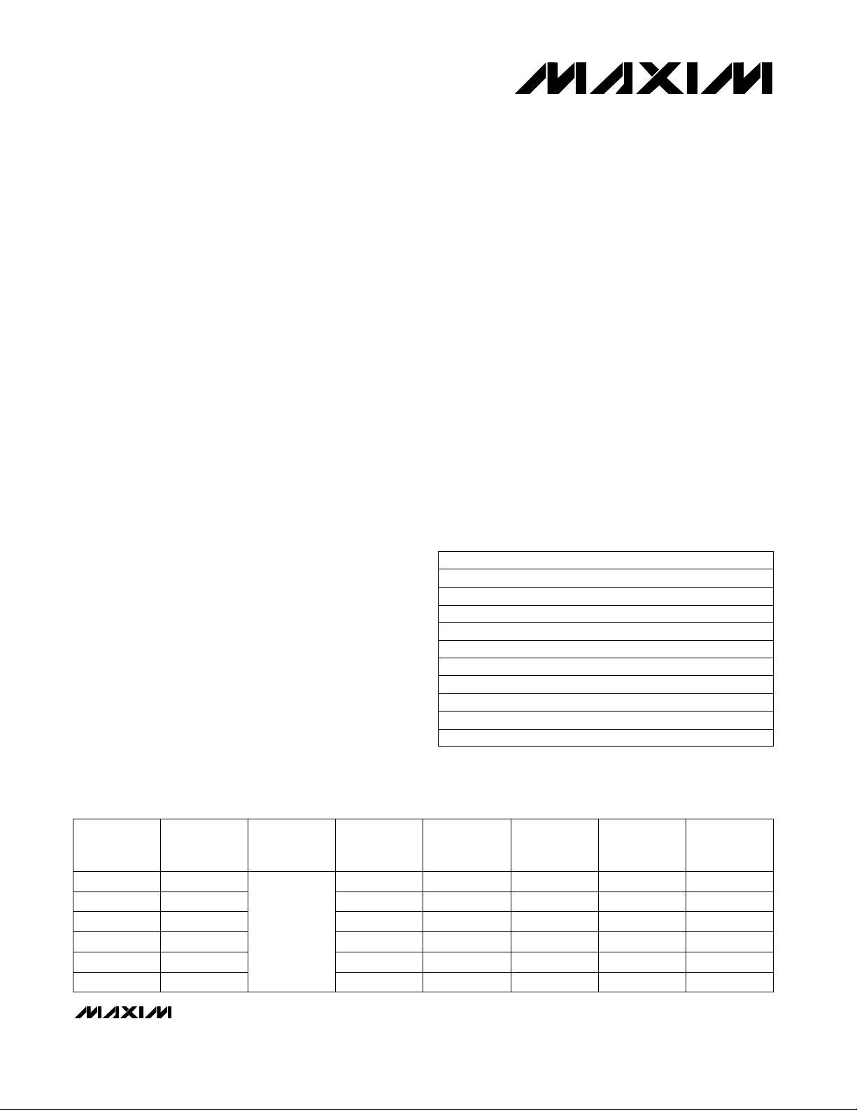
______________Ordering Information
PART
MAX3483CPA
MAX3483CSA
MAX3483C/D 0°C to +70°C
MAX3483EPA
MAX3483ESA -40°C to +85°C
MAX3485CPA
MAX3485CSA
MAX3485C/D 0°C to +70°C
MAX3485EPA
MAX3485ESA -40°C to +85°C
Ordering Information continued at end of data sheet.
* Contact factory for for dice specifications.
TEMP. RANGE PIN-PACKAGE
0°C to +70°C
0°C to +70°C
-40°C to +85°C 8 Plastic DIP
0°C to +70°C 8 Plastic DIP
0°C to +70°C
-40°C to +85°C 8 Plastic DIP
8 Plastic DIP
8 SO
Dice*
8 SO
8 SO
Dice*
8 SO
MAX3483/MAX3485/MAX3486/MAX3488/MAX3490/MAX3491
______________________________________________________________Selection Table
PART
NUMBER
MAX3483
MAX3485
MAX3486
MAX3488
MAX3490
MAX3491
GUARANTEED
DATA RATE
(Mbps)
0.25 Half Yes Yes 2 8
10 Half No Yes 2 8
2.5 Half Yes Yes 2 8
0.25 Full Yes No — 8
10 Full No No — 8
10
________________________________________________________________
SUPPLY
VOLTAGE
(V)
3.0 to 3.6
HALF/FULL
DUPLEX
Full No Yes 2 14
SLEW-RATE
LIMITED
DRIVER/
RECEIVER
ENABLE
SHUTDOWN
CURRENT
(nA)
Maxim Integrated Products
PIN
COUNT
Call toll free 1-800-998-8800 for free samples or literature.
1
3.3V-Powered, 10Mbps and Slew-Rate-Limited
True RS-485/RS-422 Transceivers
ABSOLUTE MAXIMUM RATINGS
Supply Voltage (VCC)...............................................................7V
Control Input Voltage (RE
Driver Input Voltage (DI).............................................-0.3V to 7V
Driver Output Voltage (A, B, Y, Z)..........................-7.5V to 12.5V
Receiver Input Voltage (A, B)................................-7.5V to 12.5V
Receiver Output Voltage (RO)....................-0.3V to (V
Continuous Power Dissipation (T
8-Pin Plastic DIP (derate 9.09mW/°C above +70°C) .....727mW
8-Pin SO (derate 5.88mW/°C above +70°C)..................471mW
Stresses beyond those listed under “Absolute Maximum Ratings” may cause permanent damage to the device. These are stress ratings only, and functional
operation of the device at these or any other conditions beyond those indicated in the operational sections of the specifications is not implied. Exposure to
absolute maximum rating conditions for extended periods may affect device reliability.
, DE)...................................-0.3V to 7V
+ 0.3V)
= +70°C)
A
CC
DC ELECTRICAL CHARACTERISTICS
(VCC= 3.3V ±0.3V, TA= T
MIN
to T
, unless otherwise noted. Typical values are at TA= +25°C)
MAX
14-Pin Plastic DIP (derate 10mW/°C above +70°C) ......800mW
14-Pin SO (derate 8.33mW/°C above +70°C)................667mW
Operating Temperature Ranges
MAX34_ _C_ _.......................................................0°C to +70°C
MAX34_ _E_ _....................................................-40°C to +85°C
Storage Temperature Range.............................-65°C to +160°C
Lead Temperature (soldering, 10sec).............................+300°C
UNITSMIN TYP MAXSYMBOLPARAMETER
V
V0.2∆V
V3V
V0.2∆V
V2.0V
V0.8V
µA±2I
mA
µA
1
-1
µA
V-0.2 0.2V
mV50∆V
VVCC- 0.4V
V0.4V
µA±1I
kΩ12R
Differential Driver Output
Change in Magnitude of Driver
Differential Output Voltage for
Complementary Output States
(Note 1)
Driver Common-Mode Output
Voltage
Change in Magnitude of
Common-Mode Output Voltage
(Note 1)
Input High Voltage
Input Low Voltage
Logic Input Current
Input Current (A, B)
Output Leakage (Y, Z)
Output Leakage (Y, Z)
in Shutdown Mode
Receiver Differential
Threshold Voltage
Receiver Input Hysteresis
Receiver Output High Voltage
Receiver Output Low Voltage
Three-State (High Impedance)
Output Current at Receiver
Receiver Input Resistance
V
IN1
I
IN2
I
I
OZR
CONDITIONS
RL= 100Ω (RS-422), Figure 4
RL= 54Ω (RS-485), Figure 4
OD
RL= 60Ω (RS-485), VCC= 3.3V, Figure 5
RL= 54Ω or 100Ω, Figure 4
OD
RL= 54Ω or 100Ω, Figure 4
OC
RL= 54Ω or 100Ω, Figure 4
OC
DE, DI, RE
IH
DE, DI, RE
IL
DE, DI, RE
DE = 0V,
= 0V or 3.6V
V
CC
DE = 0V, RE = 0V,
O
VCC= 0V or 3.6V, MAX3491
DE = 0V, RE = VCC,
O
VCC= 0V or 3.6V, MAX3491
-7V ≤ VCM≤ 12V
TH
VCM= 0V
TH
I
OH
OL
IN
= -1.5mA, VID= 200mV, Figure 6
OUT
I
= 2.5mA, VID= 200mV, Figure 6
OUT
VCC= 3.6V, 0V ≤ V
-7V ≤ VCM≤ 12V
OUT
≤ V
VIN= 12V
VIN= -7V
V
OUT
V
OUT
V
OUT
V
OUT
CC
= 12V
= -7V
= 12V
= -7V
2.0
1.5
1.5
1.0
-0.8
20
-20
MAX3483/MAX3485/MAX3486/MAX3488/MAX3490/MAX3491
2 _______________________________________________________________________________________
3.3V-Powered, 10Mbps and Slew-Rate-Limited
True RS-485/RS-422 Transceivers
DC ELECTRICAL CHARACTERISTICS (continued)
(VCC= 3.3V ±0.3V, TA= T
Supply Current
Supply Current in Shutdown Mode
Driver Short-Circuit Output
Current
Receiver Short-Circuit Output
Current
MIN
to T
, unless otherwise noted. Typical values are at TA= +25°C)
MAX
CONDITIONS
DE = VCC,
I
CC
SHDN
I
OSD
OSR
No load,
DI = 0V or V
DE = 0V, RE = VCC, DI = VCCor 0V
V
OUT
V
OUT
0V ≤ VRO≤ V
CC
= -7V
= 12V
CC
RE = 0V or V
DE = 0V,
RE = 0V
CC
1.1 2.2
0.95 1.9
-250
250
DRIVER SWITCHING CHARACTERISTICS—MAX3485, MAX3490, and MAX3491
(VCC= 3.3V, TA= +25°C)
CONDITIONS
Driver Differential Output Delay
Driver Differential Output Transition Time
Driver Propagation Delay, Low-to-High Level
Driver Propagation Delay, High-to-Low Level
t
- t
|
PLH
DRIVER OUTPUT ENABLE/DISABLE TIMES (MAX3485/MAX3491 only)
Driver Output Enable Time to Low Level
Driver Output Enable Time to High Level
Driver Output Disable Time from High Level
Driver Output Disable Time from Low Level RL= 110Ω, Figure 10
Driver Output Enable Time from Shutdown to Low Level
Driver Output Enable Time from Shutdown to High Level
Driver Propagation Delay Skew (Note 2)
PHL|
PLH
PHL
PDS
PZL
PZH
PHZ
PLZ
PSL
PSH
RL= 60Ω, Figure 7
DD
RL= 60Ω, Figure 7
TD
RL= 27Ω, Figure 8
RL= 27Ω, Figure 8
RL= 27Ω, Figure 8
RL= 110Ω, Figure 10
RL= 110Ω, Figure 9
RL= 110Ω, Figure 9
RL= 110Ω, Figure 10
RL= 110Ω, Figure 9
MAX3483/MAX3485/MAX3486/MAX3488/MAX3490/MAX3491
UNITSMIN TYP MAXSYMBOLPARAMETER
mA
µA0.002 1I
mA
mA±8 ±60I
UNITSMIN TYP MAXSYMBOLPARAMETER
ns12235t
ns3825t
ns72235t
ns72235t
ns8t
ns45 90t
ns45 90t
ns40 80t
ns40 80t
ns650 900t
ns650 900t
DRIVER SWITCHING CHARACTERISTICS—MAX3486
(VCC= 3.3V, TA= +25°C)
CONDITIONS
Driver Differential Output Delay
Driver Differential Output Transition Time
Driver Propagation Delay, Low-to-High Level
Driver Propagation Delay, High-to-Low Level
t
- t
|
PLH
Driver Output Enable Time to Low Level
Driver Output Enable Time to High Level
Driver Output Disable Time from High Level
Driver Output Disable Time from Low Level RL= 110Ω, Figure 10
Driver Output Enable Time from Shutdown to Low Level
Driver Output Enable Time from Shutdown to High Level
Driver Propagation Delay Skew (Note 2)
PHL|
_______________________________________________________________________________________ 3
PLH
PHL
PDS
PZL
PZH
PHZ
PLZ
PSL
PSH
RL= 60Ω, Figure 7
DD
RL= 60Ω, Figure 7
TD
RL= 27Ω, Figure 8
RL= 27Ω, Figure 8
RL= 27Ω, Figure 8
RL= 110Ω, Figure 10
RL= 110Ω, Figure 9
RL= 110Ω, Figure 9
RL= 110Ω, Figure 10
RL= 110Ω, Figure 9
UNITSMIN TYP MAXSYMBOLPARAMETER
ns24 48 70t
ns15 35 60t
ns20 48 70t
ns20 48 70t
ns11t
ns55 100t
ns55 100t
ns45 80t
ns45 80t
ns700 1000t
ns700 1000t
3.3V-Powered, 10Mbps and Slew-Rate-Limited
True RS-485/RS-422 Transceivers
DRIVER SWITCHING CHARACTERISTICS—MAX3483 and MAX3488
(VCC= 3.3V, TA= +25°C)
CONDITIONS
Driver Differential Output Delay
Driver Differential Output Transition Time
Driver Propagation Delay, Low-to-High Level
Driver Propagation Delay, High-to-Low Level
t
- t
|
PLH
DRIVER OUTPUT ENABLE/DISABLE TIMES (MAX3483 only)
Driver Output Enable Time to Low Level
Driver Output Enable Time to High Level
Driver Output Disable Time from High Level
Driver Output Disable Time from Low Level RL= 110Ω, Figure 10
Driver Output Enable Time from Shutdown to Low Level
Driver Output Enable Time from Shutdown to High Level
Driver Propagation Delay Skew (Note 2)
PHL|
PLH
PHL
PDS
PZL
PZH
PHZ
PLZ
PSL
PSH
RL= 60Ω, Figure 7
DD
RL= 60Ω, Figure 7
TD
RL= 27Ω, Figure 8
RL= 27Ω, Figure 8
RL= 27Ω, Figure 8
RL= 110Ω, Figure 10
RL= 110Ω, Figure 9
RL= 110Ω, Figure 9
RL= 110Ω, Figure 10
RL= 110Ω, Figure 9
RECEIVER SWITCHING CHARACTERISTICS
(VCC= 3.3V, TA= +25°C)
UNITSMIN TYP MAXSYMBOLPARAMETER
ns600 900 1400t
ns400 700 1200t
ns700 1000 1500t
ns700 1000 1500t
ns100t
ns900 1300t
ns600 800t
ns50 80t
ns50 80t
µs1.9 2.7t
µs2.2 3.0t
CONDITIONS
Time to Shutdown
Receiver Propagation Delay,
Low-to-High Level
Receiver Propagation Delay,
High-to-Low Level
t
- t
|
PLH
Propagation Delay Skew
Receiver Output Enable Time
to Low Level
Receiver Output Enable Time
to High Level
Receiver Output Disable
Time from High Level
Receiver Output Disable
Time from Low Level
Receiver Output Enable Time
from Shutdown to Low Level
Receiver Output Enable Time
from Shutdown to High Level
Note 1: ∆VODand ∆VOCare the changes in VODand VOC, respectively, when the DI input changes state.
Note 2: Measured on
Note 3: The transceivers are put into shutdown by bringing RE high and DE low. If the inputs are in this state for less than 80ns, the
MAX3483/MAX3485/MAX3486/MAX3488/MAX3490/MAX3491
Receiver
PHL|
t
PLH
|
parts are guaranteed not to enter shutdown. If the inputs are in this state for at least 300ns, the parts are guaranteed to
have entered shutdown. See
(Y) - t
SHDN
t
RPLH
t
RPHL
t
RPDS
PRZL
PRZH
PRHZ
PRLZ
PRSL
PRSH
PHL
MAX3483/MAX3485/MAX3486/MAX3491 only
(Note 3)
VID= 0V to 3.0V, CL= 15pF, Figure 11
MAX3483/MAX3488
VID= 0V to 3.0V, CL= 15pF, Figure 11
MAX3483/MAX3488
VID= 0V to 3.0V, CL= 15pF, Figure 11
MAX3483/MAX3488
CL= 15pF, Figure 12,
MAX3483/MAX3485/MAX3486/MAX3491 only
CL= 15pF, Figure 12,
MAX3483/MAX3485/MAX3486/MAX3491 only
CL= 15pF, Figure 12,
MAX3483/MAX3485/MAX3486/MAX3491 only
CL= 15pF, Figure 12,
MAX3483/MAX3485/MAX3486/MAX3491 only
CL= 15pF, Figure 12,
MAX3483/MAX3485/MAX3486/MAX3491 only
CL= 15pF, Figure 12,
MAX3483/MAX3485/MAX3486/MAX3491 only
(Y)|and |t
Low-Power Shutdown Mode
PLH
(Z) - t
PHL
(Z)
|.
section.
25 65 90
25 75 120
25 65 90
25 75 120
10
20
UNITSMIN TYP MAXSYMBOLPARAMETER
ns80 190 300t
ns
ns
ns
ns25 50t
ns25 50t
ns25 45t
ns25 45t
ns720 1400t
ns720 1400t
4 _______________________________________________________________________________________
3.3V-Powered, 10Mbps and Slew-Rate-Limited
True RS-485/RS-422 Transceivers
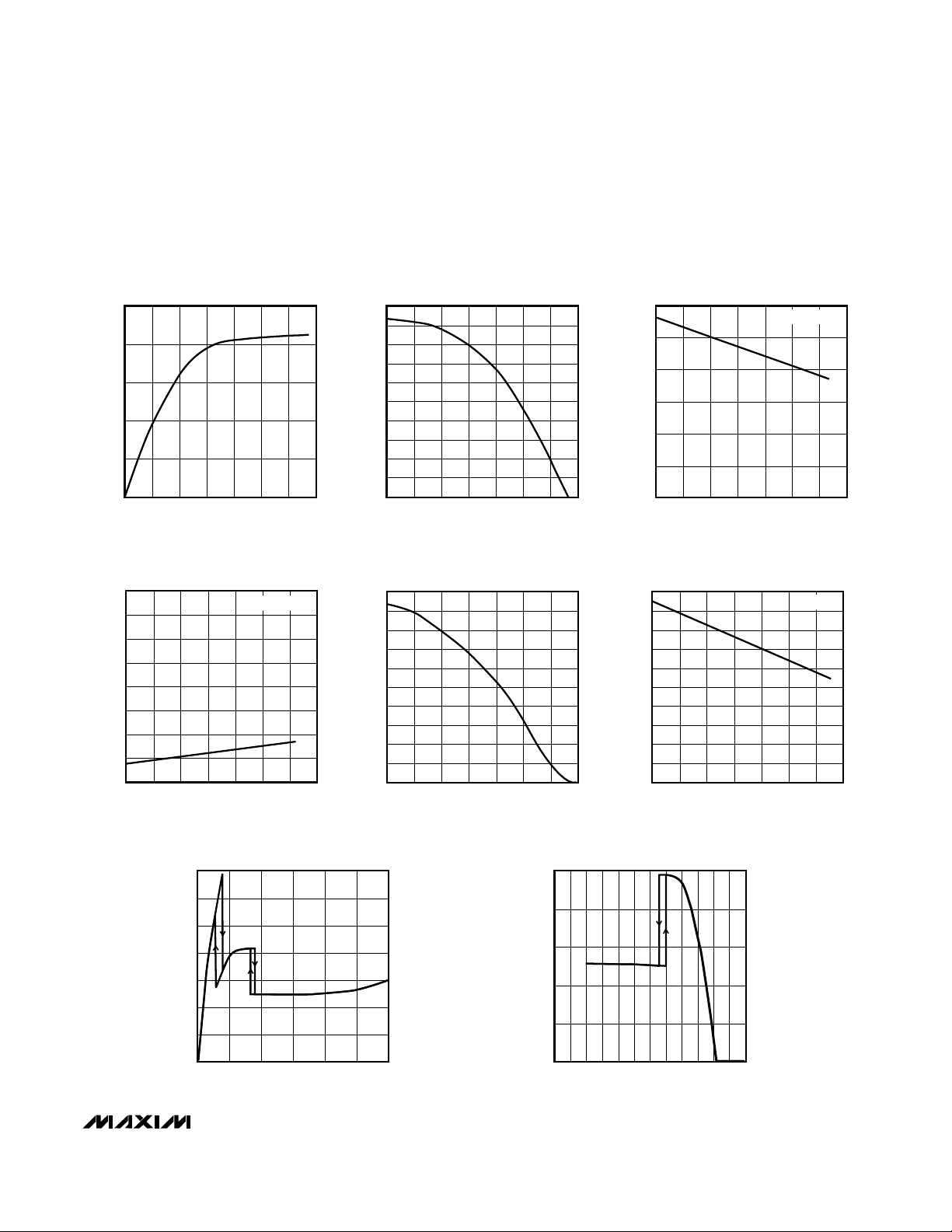
__________________________________________Typical Operating Characteristics
(VCC= 3.3V, TA= +25°C, unless otherwise noted.)
OUTPUT CURRENT vs.
RECEIVER OUTPUT LOW VOLTAGE
25
20
15
10
OUTPUT CURRENT (mA)
5
0
0 0.5 1.0 1.5 2.0 2.5 3.53.0
OUTPUT LOW VOLTAGE (V)
RECEIVER OUTPUT LOW VOLTAGE
vs. TEMPERATURE
0.8
0.7
0.6
0.5
0.4
0.3
0.2
OUTPUT LOW VOLTAGE (V)
0.1
0
-40 -20 0 20 40 60 10080
TEMPERATURE (°C)
IRO = 2.5mA
-20
-18
MAX3483-01
-16
-14
-12
-10
-8
-6
OUTPUT CURRENT (mA)
-4
-2
0
0 0.5 1.0 1.5 2.0 2.5 3.53.0
100
90
MAX3483-04
80
70
60
50
40
30
OUTPUT CURRENT (mA)
20
10
0
0 0.5 1.0 1.5 2.0 2.5 3.53.0
OUTPUT CURRENT vs.
RECEIVER OUTPUT HIGH VOLTAGE
MAX3483-02
OUTPUT HIGH VOLTAGE (V)
OUTPUT HIGH VOLTAGE (V)
DRIVER OUTPUT CURRENT vs.
DIFFERENTIAL OUTPUT VOLTAGE
MAX3483-05
DIFFERENTIAL OUTPUT VOLTAGE (V)
DIFFERENTIAL OUTPUT VOLTAGE (V)
RECEIVER OUTPUT HIGH VOLTAGE
vs. TEMPERATURE
3.30
3.25
3.20
3.15
3.10
3.05
3.00
-40 -20 0 20 40 60 10080
TEMPERATURE (°C)
DRIVER DIFFERENTIAL OUTPUT
VOLTAGE vs.TEMPERATURE
2.6
2.5
2.4
2.3
2.2
2.1
2.0
1.9
1.8
1.7
1.6
-40 -20 0 20 40 60 10080
TEMPERATURE (°C)
IRO = 1.5mA
R = 54Ω
MAX3483/MAX3485/MAX3486/MAX3488/MAX3490/MAX3491
MAX3483-03
MAX3483-06
OUTPUT CURRENT vs.
DRIVER OUTPUT LOW VOLTAGE
175
150
125
100
75
50
OUTPUT CURRENT (mA)
25
0
0246 81012
OUTPUT LOW VOLTAGE (V)
_______________________________________________________________________________________
MAX3483-07
OUTPUT CURRENT vs.
DRIVER OUTPUT HIGH VOLTAGE
-100
-80
-60
-40
OUTPUT CURRENT (mA)
-20
0
-7 -6 -3-4-5 -2 -1
OUTPUT HIGH VOLTAGE (V)
MAX3483-08
543210
5

3.3V-Powered, 10Mbps and Slew-Rate-Limited
True RS-485/RS-422 Transceivers
_____________________________Typical Operating Characteristics (continued)
SUPPLY CURRENT
vs. TEMPERATURE
1.2
1.1
1.0
0.9
SUPPLY CURRENT (mA)
0.8
0.7
-40 -20 0 20 40 60 10080
DE = 0, RE = 0
TEMPERATURE (°C)
X = DON’T CARE
DE = VCC, RE = X
MAX3483-09
100
90
80
70
60
50
40
30
SHUTDOWN CURRENT (nA)
20
10
0
-40 -20 0 20 40 60 10080
SHUTDOWN CURRENT
vs. TEMPERATURE
MAX3483-10
TEMPERATURE (°C)
______________________________________________________________Pin Description
PIN
MAX3483/
MAX3485/
MAX3486
2
3
4
5
—
—
6
—
7
—
8
MAX3483/MAX3485/MAX3486/MAX3488/MAX3490/MAX3491
—
MAX3488/
MAX3490
21
—
—
3
4
5
6
—
8
—
7
1
—
MAX3491
2
3
4
5
6, 7 Ground
9 Noninverting Driver Output
10 Inverting Driver Output
— Noninverting Receiver Input and Noninverting Driver Output
12 Noninverting Receiver Input
— B Inverting Receiver Input and Inverting Driver Output
11 B Inverting Receiver Input
13, 14 V
1, 8 N.C. No Connect—not internally connected
NAME
NAME
RO
–
RE
DE
DI
GND
Y
Z
A
A
CC
FUNCTION
FUNCTION
Receiver Output. If A > B by 200mV, RO will be high; if A < B by 200mV,
RO will be low.
Receiver Output Enable. RO is enabled when RE is low; RO is high impedance when RE
is high. If RE is high and DE is low, the device will enter a
low-power shutdown mode.
Driver Output Enable. The driver outputs are enabled by bringing DE high.
They are high impedance when DE is low. If RE is high and DE is low, the
device will enter a low-power shutdown mode. If the driver outputs are
enabled, the parts function as line drivers. While they are high impedance,
they function as line receivers if RE
is low.
Driver Input. A low on DI forces output Y low and output Z high. Similarly, a
high on DI forces output Y high and output Z low.
Positive Supply: 3.0V ≤ VCC≤ 3.6V
6 _______________________________________________________________________________________

3.3V-Powered, 10Mbps and Slew-Rate-Limited
True RS-485/RS-422 Transceivers
TOP VIEW
MAX3483
MAX3485
RO
2
RE
3
DE
4
DI
D
8
V
CC
7
B
6
A
5
GND
R
1
RO
RE
DE
DI
R
1
2
3
4
D
8
V
CC
B
7
Rt
6
A
5
GND
MAX3486
B
Rt
A
DE
D
R
MAX3483/MAX3485/MAX3486/MAX3488/MAX3490/MAX3491
DI
RO
DIP/SO
NOTE: PIN LABELS Y AND Z ON TIMING, TEST, AND WAVEFORM DIAGRAMS REFER TO PINS A AND B WHEN DE IS HIGH.
Figure 1. MAX3483/MAX3485/MAX3486 Pin Configuration and Typical Operating Circuit
V
TOP VIEW
V
GND
3
A
1
CC
RO
DI
R
2
3
4
D
8
B
7
6
Z
Y
5
DI
2
RO
CC
1
Y
5
DR
6
Z
8
A
R
Rt
7
B
MAX3488
MAX3490
DIP/SO
4
GND
Figure 2. MAX3488/MAX3490 Pin Configuration and Typical Operating Circuit
RE
V
CC
Rt
D
GND
RO
DI
TOP VIEW
N.C.
RO
RE
DE
GND
GND
14
13
12
11
10
V
CC
V
CC
A
B
Z
9
Y
8
N.C.
N.C.
DI
RO
1, 8
1
2
3
4
5
DI
6
7
R
D
DIP/SO
DE V
5
D
2
3 6, 7
RE GND
Figure 3. MAX3491 Pin Configuration and Typical Operating Circuit
_______________________________________________________________________________________ 7
CC
13, 144
9
Y
10
Z
12
A
RD
11
B
MAX3491
Rt
VCCRE
Rt
R
GND DE
RO
DI

3.3V-Powered, 10Mbps and Slew-Rate-Limited
True RS-485/RS-422 Transceivers
375Ω
R
L
2
V
D
V
CC
OD
R
L
V
OC
2
V
D
CC
V
OD
R
L
375Ω
VCM =
-7V to +12V
Figure 4. Driver VODand V
V
ID
R
0V
OC
V
OL
Figure 6. Receiver VOHand V
D
GENERATOR
(NOTE 4)
50Ω
V
Figure 5. Driver VODwith Varying Common-Mode Voltage
V
I
(+)
OL
C
L
CC
C
L
OH
OL
R
60Ω
= 15pF (NOTE 5)
C
L
I
OH
(-)
3V
IN
OUT
=
L
OUT
1.5V
t
DO
90%
50%
10%
t
TD
1.5V
90%
0V
t
DO
≈ 2.0V
50%
10%
t
TD
≈ -2.0V
Figure 7. Driver Differential Output Delay and Transition Times
MAX3483/MAX3485/MAX3486/MAX3488/MAX3490/MAX3491
8 _______________________________________________________________________________________

3.3V-Powered, 10Mbps and Slew-Rate-Limited
True RS-485/RS-422 Transceivers
MAX3483/MAX3485/MAX3486/MAX3488/MAX3490/MAX3491
D
GENERATOR
(NOTE 4)
50Ω
V
CC
V
OM
Figure 8. Driver Propagation Times
S1
D0V OR 3V
= 50pF
C
L
GENERATOR
(NOTE 4)
50Ω
(NOTE 5)
VOH + V
=
V
OM
S1
2
=
OL
VOH + V
2
≈ 1.5V
OL
V
R
L
≈ 1.5V
OM
R
= 27Ω
L
CL = 15pF
(NOTE 5)
OUT
= 110Ω
OUT
IN
OUT
OUT
OUT
3V
1.5V
t
PLH
Y
Z
IN
V
OM
t
PHL
V
OM
1.5V
t
PZH
V
OM
1.5V
1.5V
0V
t
PHL
V
OH
V
OM
V
OL
t
PLH
V
OH
V
OM
V
OL
3V
0V
t
PHZ
V
OH
0.25V
0V
Figure 9. Driver Enable and Disable Times (t
V
CC
S1
0V OR 3V
GENERATOR
(NOTE 4)
D
CL = 50pF
(NOTE 5)
50Ω
Figure 10. Driver Enable and Disable Times (t
_______________________________________________________________________________________ 9
PZH
PZL
, t
PSH
RL = 110Ω
OUT
, t
PSL
, t
)
PHZ
3V
IN
OUT
, t
)
PLZ
t
1.5V
PSL
V
OM
1.5V
0V
t
PLZ
V
CC
0.25V
V
OL

3.3V-Powered, 10Mbps and Slew-Rate-Limited
True RS-485/RS-422 Transceivers
V
ID
GENERATOR
(NOTE 4)
1.5V
0V
50Ω
R
Figure 11. Receiver Propagation Delay
t
PRZH
tPRSH
S3
GENERATOR
(NOTE 4)
1.5V
1.5V
1.5V
-1.5V
IN
OUT
CC
OL
3.0V
0V
V
CC
0V
S1 CLOSED
S2 OPEN
S3 = -1.5V
OUT
C
= 15pF
L
(NOTE 5)
V
CC
=
V
OM
2
V
ID
R
CL
(NOTE 5)
50Ω
3V
S1 OPEN
S2 CLOSED
S3 = 1.5V
0V
V
OH
0V
IN
t
RPLH
OUT
1k
IN
OUT
1.5V
S1
S2
V
OM
t
PRZL
tPRSL
1.5V
1.5V
t
RPHL
V
OM
V
CC
3V
1.5V
0V
V
V
3V
0V
V
V
S1 CLOSED
S2 OPEN
S3 = -1.5V
CC
OL
OUT
3V
0V
V
0V
OH
S1 OPEN
S2 CLOSED
S3 = 1.5V
OUT
IN
1.5V
t
PRLZ
0.25V
IN
0.25V
1.5V
t
PRHZ
Figure 12. Receiver Enable and Disable Times
Note 4: The input pulse is supplied by a generator with the following characteristics: PRR = 250kHz, 50% duty cycle, tr≤ 6.0ns, ZO= 50Ω.
Note 5: C
MAX3483/MAX3485/MAX3486/MAX3488/MAX3490/MAX3491
includes probe and stray capacitance.
L
10 ______________________________________________________________________________________

3.3V-Powered, 10Mbps and Slew-Rate-Limited
True RS-485/RS-422 Transceivers
____________________Function Tables
Devices with Receiver/Driver Enable
(MAX3483/MAX3485/MAX3486/MAX3491)
Table 1. Transmitting
INPUTS OUTPUTS
RE DE DI B* A*
X 1 1 0 1 Normal
X 1 0 1 0 Normal
0 0 X High-Z High-Z Normal
1 0 X High-Z High-Z Shutdown
* B and A outputs are Z and Y, respectively, for full-duplex part
(MAX3491).
X = Don’t care; High-Z = High impedance
Table 2. Receiving
INPUTS
RE DE A, B RO
0 0* ≥ +0.2V 1 Normal
0 0* ≤-0.2V 0 Normal
0 0* Inputs Open 1 Normal
1 0 X High-Z Shutdown
* DE is a “don’t care” (x) for the full-duplex part (MAX3491).
X = Don’t care; High-Z = High impedance
Devices without Receiver/Driver Enable
OUTPUTS
(MAX3488/MAX3490)
Table 3. Transmitting Table 4. Receiving
INPUT OUTPUTS
DI Z Y
1 0 1
0 1 0
INPUTS OUTPUT
A, B RO
≥+0.2V 1
≤-0.2V 0
Inputs Open 1
MODE
MODE
__________Applications Information
The MAX3483/MAX3485/MAX3486/MAX3488/MAX3490/
MAX3491 are low-power transceivers for RS-485 and
RS-422 communications. The MAX3483 and MAX3488
can transmit and receive at data rates up to 250kbps,
the MAX3486 at up to 2.5Mbps, and the MAX3485/
MAX3490/MAX3491 at up to 10Mbps. The MAX3488/
MAX3490/MAX3491 are full-duplex transceivers, while
the MAX3483/MAX3485/MAX3486 are half-duplex.
Driver Enable (DE) and Receiver Enable (RE) pins are
included on the MAX3483/MAX3485/MAX3486/
MAX3491. When disabled, the driver and receiver outputs are high impedance.
Reduced EMI and Reflections
(MAX3483/MAX3486/MAX3488)
The MAX3483/MAX3488 are slew-rate limited, minimizing EMI and reducing reflections caused by improperly
terminated cables. Figure 13 shows both the driver
output waveform of a MAX3485/MAX3490/MAX3491
transmitting a 125kHz signal and the Fourier analysis of
that waveform. High-frequency harmonics with large
amplitudes are evident. Figure 14 shows the same information, but for the slew-rate-limited MAX3483/MAX3488
transmitting the same signal. The high-frequency harmonics have much lower amplitudes, and the potential for
EMI is significantly reduced.
Low-Power Shutdown Mode
(MAX3483/MAX3485/MAX3486/MAX3491)
A low-power shutdown mode is initiated by bringing both
RE high and DE low. The devices will not shut down
unless both the driver and receiver are disabled (high
impedance). In shutdown, the devices typically draw
only 2nA of supply current.
For these devices, the t
assume the part was in the low-power shutdown mode;
the t
PZH
and t
enable times assume the receiver or
PZL
driver was disabled, but the part was not shut down.
PSH
and t
enable times
PSL
MAX3483/MAX3485/MAX3486/MAX3488/MAX3490/MAX3491
10dB/div
5MHz500kHz/div0Hz
Figure 13. Driver Output Waveform and FFT Plot of MAX3485/
MAX3490/MAX3491 Transmitting a 125kHz Signal
______________________________________________________________________________________ 11
10dB/div
5MHz500kHz/div0Hz
Figure 14. Driver Output Waveform and FFT Plot of MAX3483/
MAX3488 Transmitting a 125kHz Signal

3.3V-Powered, 10Mbps and Slew-Rate-Limited
True RS-485/RS-422 Transceivers
B
1V/div
DI
2V/div
Z
1V/div
A
1V/div
Y
1V/div
20ns/div
Figure 15. MAX3485/MAX3490/MAX3491 Driver Propagation
Delay
DI
2V/div
Z
1V/div
Y
1V/div
1µs/div
Figure 17. MAX3483/MAX3488 Driver Propagation Delay
RO
2V/div
20ns/div
Figure 16. MAX3485/MAX3490/MAX3491 Receiver
Propagation Delay Driven by External RS-485 Device
B
1V/div
A
1V/div
RO
2V/div
1µs/div
Figure 18. MAX3483/MAX3488 Receiver Propagation Delay
DI
5V/div
VY - V
Z
2V/div
RO
5V/div
2µs/div
Figure 19. MAX3483/MAX3488 System Differential Voltage at
125kHz Driving 4000 ft of Cable
DI
5V/div
VY - V
Z
2V/div
RO
5V/div
2µs/div
Figure 20. MAX3485/MAX3490/MAX3491 System Differential
Voltage at 125kHz Driving 4000 ft of Cable
MAX3483/MAX3485/MAX3486/MAX3488/MAX3490/MAX3491
12 ______________________________________________________________________________________

3.3V-Powered, 10Mbps and Slew-Rate-Limited
True RS-485/RS-422 Transceivers
MAX3483/MAX3485/MAX3486/MAX3488/MAX3490/MAX3491
120Ω
DI
D
DE
RO
RE
Figure 21. MAX3483/MAX3485/MAX3486 Typical RS-485 Network
R
MAX3483
MAX3485
MAX3486
B
A
B
A
R
D
DI RO DE
DE
Driver Output Protection
Excessive output current and power dissipation caused
by faults or by bus contention are prevented by two
mechanisms. A foldback current limit on the output stage
provides immediate protection against short circuits over
the whole common-mode voltage range (see
Operating Characteristics
). In addition, a thermal shut-
Typical
down circuit forces the driver outputs into a high-impedance state if the die temperature rises excessively.
Propagation Delay
Figures 15–18 show the typical propagation delays. Skew
time is simply the difference between the low-to-high and
high-to-low propagation delay. Small driver/receiver
skew times help maintain a symmetrical mark-space
ratio (50% duty cycle).
The receiver skew time, |t
(20ns for the MAX3483/MAX3488). The driver skew
times are 8ns for the MAX3485/MAX3490/MAX3491,
11ns for the MAX3486, and typically under 100ns for
the MAX3483/MAX3488.
PRLH
- t
, is under 10ns
PRHL|
120Ω
B
D
B
A
R
D
DI
RO
A
R
RERE
DE
DI
RO
RE
Line Length vs. Data Rate
The RS-485/RS-422 standard covers line lengths up to
4000 feet. For line lengths greater than 4000 feet, see
Figure 23.
Figures 19 and 20 show the system differential voltage
for parts driving 4000 feet of 26AWG twisted-pair wire
at 125kHz into 120Ω loads.
Typical Applications
The MAX3483, MAX3485, MAX3486, MAX3488,
MAX3490, and MAX3491 transceivers are designed for
bidirectional data communications on multipoint bus
transmission lines. Figures 21 and 22 show typical network applications circuits. These parts can also be
used as line repeaters, with cable lengths longer than
4000 feet, as shown in Figure 23.
To minimize reflections, the line should be terminated at
both ends in its characteristic impedance, and stub
lengths off the main line should be kept as short as
possible. The slew-rate-limited MAX3483/MAX3488
and the partially slew-rate-limited MAX3486 are more
tolerant of imperfect termination.
______________________________________________________________________________________ 13

3.3V-Powered, 10Mbps and Slew-Rate-Limited
True RS-485/RS-422 Transceivers
A
RO
RE
DE
DI
R
D
120Ω
B
Z
120Ω
Y
Z
Y
AA
BB
R
D
DI DIRO RO
DE DE
RE
NOTE: RE AND DE ON MAX3491 ONLY.
Figure 22. MAX3488/MAX3490/MAX3491 Full-Duplex RS-485 Network
MAX3488
MAX3490
120Ω
120Ω
MAX3491
DATA IN
DATA OUT
RO
RE
DE
DI
R
D
A
B
Z
Y
Y
120Ω
Z
B
120Ω
Z
Y
A
D
R
R
D
MAX3488
MAX3490
MAX3491
RE
DI
DE
RE
RO
NOTE: RE AND DE ON MAX3491 ONLY.
Figure 23. Line Repeater for MAX3488/MAX3490/MAX3491
MAX3483/MAX3485/MAX3486/MAX3488/MAX3490/MAX3491
14 ______________________________________________________________________________________

3.3V-Powered, 10Mbps and Slew-Rate-Limited
True RS-485/RS-422 Transceivers
PART
MAX3486CPA
MAX3486CSA
MAX3486C/D 0°C to +70°C
MAX3486EPA
MAX3486ESA -40°C to +85°C
MAX3488CPA
MAX3488CSA
MAX3488C/D 0°C to +70°C
MAX3488EPA
MAX3488ESA -40°C to +85°C
MAX3490CPA
MAX3490CSA
MAX3490C/D 0°C to +70°C
MAX3490EPA
MAX3490ESA -40°C to +85°C
MAX3491CPD
MAX3491CSD
MAX3491C/D 0°C to +70°C
MAX3491EPD
MAX3491ESD -40°C to +85°C
* Contact factory for for dice specifications.
TEMP. RANGE PIN-PACKAGE
0°C to +70°C
0°C to +70°C
-40°C to +85°C 8 Plastic DIP
0°C to +70°C 8 Plastic DIP
0°C to +70°C
-40°C to +85°C 8 Plastic DIP
0°C to +70°C 8 Plastic DIP
0°C to +70°C
-40°C to +85°C 8 Plastic DIP
0°C to +70°C 14 Plastic DIP
0°C to +70°C
-40°C to +85°C 14 Plastic DIP
8 Plastic DIP
8 SO
Dice*
8 SO
8 SO
Dice*
8 SO
8 SO
Dice*
8 SO
14 SO
Dice*
14 SO
__________________ Chip Topography_Ordering Information (continued)
GND
RO
RE
DE
DI
V
CC
0.086"
(2.18mm)
GND
MAX3483/MAX3485/MAX3486/MAX3488/MAX3490/MAX3491
A
B
Z/B
0.146"
(3.71mm)
Y/A
TRANSISTOR COUNT: 810
SUBSTRATE CONNECTED TO GROUND
______________________________________________________________________________________ 15

3.3V-Powered, 10Mbps and Slew-Rate-Limited
True RS-485/RS-422 Transceivers
________________________________________________________Package Information
DIM
D
A
0.101mm
e
A1
B
0.004in.
C
L
0°-8°
SO
HE
SMALL OUTLINE
PACKAGE
(0.150 in.)
E
D
A3
A2
A
L
A1
e
B1
B
E1
0° - 15°
C
eA
eB
A
A1
B
C
E
H
DIM
D
D
D
DIM
A1
A2
A3
B1
D1
E1
eA
eB
D1
Plastic DIP
PLASTIC
DUAL-IN-LINE
PACKAGE
(0.300 in.)
DIM
D
D
D
D
D
D
INCHES MILLIMETERS
0.053
0.004
0.014
0.007
0.150
e
0.228
L
0.016
PINS
14
16
A
0.015
0.125
0.055
B
0.016
0.045
C
0.008
0.005
E
0.300
0.240
e
0.100
0.300
L
0.115
PINS
14
16
18
20
24
MAX
MIN
0.069
0.010
0.019
0.010
0.157
8
MIN
–
–
8
0.244
0.050
INCHES MILLIMETERS
MIN
MAX
0.189
0.197
0.337
0.344
0.386
0.394
INCHES MILLIMETERS
MAX
0.200
–
0.175
0.080
0.022
0.065
0.012
0.080
0.325
0.310
–
–
0.400
0.150
INCHES MILLIMETERS
MIN
MAX
0.348
0.390
0.735
0.765
0.745
0.765
0.885
0.915
1.015
1.045
1.14
1.265
MIN
1.35
0.10
0.35
0.19
3.80
5.80
0.40
MIN
–
0.38
3.18
1.40
0.41
1.14
0.20
0.13
7.62
6.10
2.54
7.62
–
2.92
18.67
18.92
22.48
25.78
28.96
MIN
4.80
8.55
9.80
MIN
8.84
1.270.050
MAX
1.75
0.25
0.49
0.25
4.00
6.20
1.27
MAX
5.00
8.75
10.00
21-0041A
MAX
5.08
–
4.45
2.03
0.56
1.65
0.30
2.03
8.26
7.87
–
–
10.16
3.81
MAX
9.91
19.43
19.43
23.24
26.54
32.13
Maxim cannot assume responsibility for use of any circuitry other than circuitry entirely embodied in a Maxim product. No circuit patent licenses are
Maxim cannot assume responsibility for use of any circuitry other than circuitry entirely embodied in a Maxim product. No circuit patent licenses are
Maxim cannot assume responsibility for use of any circuitry other than circuitry entirely embodied in a Maxim product. No circuit patent licenses are
MAX3483/MAX3485/MAX3486/MAX3488/MAX3490/MAX3491
implied. Maxim reserves the right to change the circuitry and specifications without notice at any time.
implied. Maxim reserves the right to change the circuitry and specifications without notice at any time.
implied. Maxim reserves the right to change the circuitry and specifications without notice at any time.
16
__________________Maxim Integrated Products, 120 San Gabriel Drive, Sunnyvale, CA 94086 (408) 737-7600
16
__________________Maxim Integrated Products, 120 San Gabriel Drive, Sunnyvale, CA 94086 (408) 737-7600
16
__________________Maxim Integrated Products, 120 San Gabriel Drive, Sunnyvale, CA 94086 (408) 737-7600
© 1994 Maxim Integrated Products Printed USA is a registered trademark of Maxim Integrated Products.
© 1994 Maxim Integrated Products Printed USA is a registered trademark of Maxim Integrated Products.
© 1994 Maxim Integrated Products Printed USA is a registered trademark of Maxim Integrated Products.
 Loading...