

Page 1
General Description
The MAX3480EA/MAX3480EB are electrically isolated
RS-485/RS-422 data-communications interfaces. The
RS-485/RS-422 I/O pins are protected against ±15kV
electrostatic discharge (ESD) shocks, without latchup.
Transceivers, optocouplers, and a transformer are all
included in one low-cost, 28-pin PDIP package. A single +3.3V supply on the logic side powers both sides
of the interface.
The MAX3480EB features reduced-slew-rate drivers
that minimize EMI and reduce reflections caused by
improperly terminated cables, allowing error-free data
transmission at data rates up to 160kbps. The
MAX3480EA’s driver slew rate is not limited, allowing
transmission rates up to 2.5Mbps.
Drivers are short-circuit current limited and are protected against excessive power dissipation by thermal
shutdown circuitry that places the driver outputs into a
high-impedance state. The receiver input has a fail-safe
feature that guarantees a logic-high output if the input
is open circuit.
The MAX3480EA/MAX3480EB are guaranteed to withstand 1260V
RMS
(1min) or 1520V
RMS
(1s). Their isolated
inputs and outputs meet RS-485/RS-422 specifications.
________________________Applications
Isolated RS-485/RS-422 Data Interface
Transceivers for EMI-Sensitive Applications
Industrial-Control Local Area Networks
Automatic Test Equipment
HVAC/Building Control Networks
Telecom
____________________________Features
♦ Isolated Data Interface Guaranteed to 1260V
RMS
(1min)
♦ ±15kV ESD Protection for I/O Pins
♦ Slew-Rate-Limited Data Transmission (160kbps for
MAX3480EB)
♦ High-Speed, Isolated, 2.5Mbps RS-485 Interface
(MAX3480EA)
♦ Single +3.3V Supply
♦ Current Limiting and Thermal Shutdown for
Driver Overload Protection
♦ Standard 28-Pin PDIP Package
♦ Allows Up to 128 Transceivers on the Bus
MAX3480EA/MAX3480EB
±15kV ESD-Protected, Isolated, 3.3V
RS-485/RS-422 Data Interfaces
________________________________________________________________ Maxim Integrated Products 1
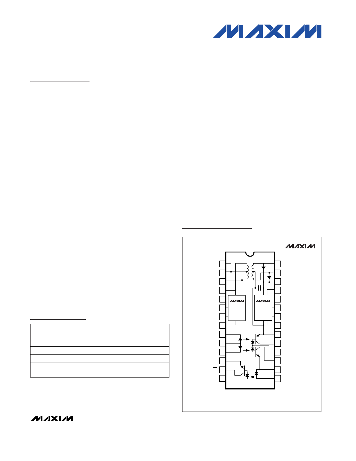
28
27
26
25
24
23
22
21
1
2
3
4
5
6
7
8
AC1
AC2
ISO V
CC1
B
D2
D1
V
CC2
V
CC1
ISO RO DRV
A
ISO DI IN
ISO DE INV
CC3
SD
FS
GND1
20
19
18
17
9
10
11
12
ISO COM1
ISO DI DRV
ISO V
CC2
ISO DE DRV
GND2
DE
V
CC4
DI
16
15
13
14
ISO COM2
ISO RO LED
V
CC5
RO
MAX1487E
MAX487E
ISOLATION BARRIER
TOP VIEW
MAX3480EA
MAX3480EB
PDIP
MAX845
Pin Configuration
19-1941; Rev 1; 3/06
Ordering Information
PART
TEMP
RANGE
PI N -
D A T A
PKG
CODE
MAX3480EACPI
28 PDIP
P28M-1
MAX3480EAEPI
28 PDIP
P28M-1
MAX3480EBCPI
28 PDIP
P28M-1
MAX3480EBEPI
28 PDIP
P28M-1
*See the Reliability section at end of data sheet.
For pricing, delivery, and ordering information, please contact Maxim/Dallas Direct! at
1-888-629-4642, or visit Maxim’s website at www.maxim-ic.com.
0°C to + 70°C
- 40°C to + 85°C
0°C to + 70°C
- 40°C to + 85°C
PA C K A G E*
R A T E
( k b p s )
2500
2500
250
250
Page 2
MAX3480EA/MAX3480EB
±15kV ESD-Protected, Isolated, 3.3V
RS-485/RS-422 Data Interfaces
2 _______________________________________________________________________________________
ABSOLUTE MAXIMUM RATINGS
ELECTRICAL CHARACTERISTICS
(VCC= V
CC1
= V
CC2
= V
CC4
= V
CC5
= +3.0V to +3.6V, FS = 0, TA= T
MIN
to T
MAX
, unless otherwise noted. Typical values are at V
CC
=
+3.3V and T
A
= +25°C.) (Notes 1, 2)
Stresses beyond those listed under “Absolute Maximum Ratings” may cause permanent damage to the device. These are stress ratings only, and functional
operation of the device at these or any other conditions beyond those indicated in the operational sections of the specifications is not implied. Exposure to
absolute maximum rating conditions for extended periods may affect device reliability.
With Respect to GND
Supply Voltage (V
CC
1,
V
CC
2,
V
CC
4,
V
CC
5
) .......-0.3V to +3.8V
Supply Voltage (V
CC3
) ........................................-0.3V to +7V
Control Input Voltage (SD, FS) ............-0.3V to (V
CC3
+ 0.3V)
Receiver Output Voltage (RO).............-0.3V to (V
CC5
+ 0.3V)
With Respect to ISO COM
Control Input Voltage (ISO DE _)......-0.3V to (ISO V
CC_
+ 0.3V)
Driver Input Voltage (ISO DI _) .....-0.3V to (ISO V
CC_
+ 0.3V)
Receiver Output Voltage (ISO RO _) ..-0.3V to (ISO V
CC_
+ 0.3V)
Driver Output Voltage (A, B)..............................-8V to +12.5V
Receiver Input Voltage (A, B)............................-8V to +12.5V
LED Forward Current (DI, DE, ISO RO LED) ......................50mA
Continuous Power Dissipation (T
A
= +70°C)
28-Pin PDIP (derate 9.09mW/°C above +70°C)............727mW
Operating Temperature Ranges
MAX3480E_CPI..................................................0°C to +70°C
MAX3480E_EPI...............................................-40°C to +85°C
Storage Temperature Range .............................-65°C to +150°C
Lead Temperature (soldering, 10s) .................................+300°C
PARAMETER
CONDITIONS
UNITS
f
SWL
FS = 0 60
Switch Frequency
f
SWH
FS = VCC or open
kHz
RL = ∞
MAX3480EA,
DE´ = V
CC
or open
R
L
= 54Ω
RL = ∞ 80
Operating Supply Current I
CC
MAX3480EB,
DE´ = V
CC
or open
R
L
= 54Ω
mA
Shutdown Supply Current (Note 3)
I
SHDN
SD = V
CC3
0.2 µA
V
FSH
High 2.4
FS Input Threshold
V
FSL
Low 0.8
V
FS Input Pullup Current I
FSL
FS low 50 µA
FS Input Leakage Current I
FSM
FS high 10 pA
Input High Voltage V
IH
DE´, DI´, Figure 1 VCC - 0.4 V
Input Low Voltage V
IL
DE´, DI´, Figure 1 0.4 V
Isolation Voltage V
ISO
TA = +25°C, 1min (Note 4)
V
RMS
V
SDH
High 2.4 1
Shutdown Input Threshold
V
SDL
Low 1 0.8
V
Isolation Resistance R
ISO
TA = +25°C, V
ISO
= ±50VDC
MΩ
Isolation Capacitance C
ISO
f = 1MHz 10 pF
ESD Protection ESD
A, B, Y, and Z pins, tested at Human Body
Model
kV
Differential Driver Output
(No Load)
V
OD1
8V
R = 50Ω (RS-422) 2
Differential Driver Output V
OD2
R = 27Ω (RS-485), Figure 3 1.5 5.0
V
Differential 0.3
Change in Magnitude of Driver
Output Voltage for Complementary
Output States
∆V
OD
R = 27Ω or 50Ω,
Figure 3
Common mode 0.3
V
SYMBOL
MIN TYP MAX
900
130 250
220
180
1260
100 10,000
±15
200
Page 3
MAX3480EA/MAX3480EB
±15kV ESD-Protected, Isolated, 3.3V
RS-485/RS-422 Data Interfaces
_______________________________________________________________________________________ 3
ELECTRICAL CHARACTERISTICS (continued)
(VCC= V
CC1
= V
CC2
= V
CC4
= V
CC5
= +3.0V to +3.6V, FS = 0, TA= T
MIN
to T
MAX
, unless otherwise noted. Typical values are at V
CC
=
+3.3V and T
A
= +25°C.) (Notes 1, 2)
SWITCHING CHARACTERISTICS—MAX3480EA
(VCC= V
CC1
= V
CC2
= V
CC4 =VCC5
= +3.0V to +3.6V, FS = 0, TA= T
MIN
to T
MAX
, unless otherwise noted. Typical values are at
V
CC
= +3.3V and TA= +25°C.)
ns
PARAMETER SYMBOL MIN TYP MAX UNITS
t
PLH
-
t
PHL
Differential
Receiver Skew
Driver Input to Output
Propagation Delay
t
PLH 100 275
ns
Driver Output Skew
t
SKEW 25 100 ns
Driver Rise or Fall Time
tR, t
F 15 50 ns
Driver Enable to Output High
t
ZH 0.5 1.8 µs
Driver Enable to Output Low
t
ZL 0.5 1.8 µs
Driver Disable Time from High
t
HZ 0.6 1.8 µs
CONDITIONS
Figures 4, 6; R
DIFF
= 54Ω,
CL1= CL2= 100pF
Figures 5, 7; CL= 100pF, S2 closed
Figures 5, 7; CL= 100pF, S1 closed
Figures 4, 6; R
DIFF
= 54Ω,
CL1= CL2= 100pF (Note 5)
Figures 4, 6; R
DIFF
= 54Ω,
CL1= CL2= 100pF
Figures 5, 7; CL= 15pF, S2 closed
Driver Disable Time from Low
t
LZ 0.6 1.8 µsFigures 5, 7; C
L
= 15pF, S1 closed
t
SKD
100 225
Receiver Input to Output
Propagation Delay
t
PLH
ns
Figures 4, 8; R
DIFF
= 54Ω,
C
L1
= CL2= 100pF
20 100
Figures 4, 8; R
DIFF
= 54Ω,
C
L1
= CL2= 100pF
Maximum Data Rate
f
MAX 2.5 Mbps
t
SKEW, tSKD ≤ 25% of data period
t
PHL
t
PHL 100 275
120 225
Driver Common-Mode Output V
Input Current (A, B) ISO I
Receiver Input Resistance R
Receiver Differential Threshold V
Receiver Input Hysteresis ∆V
Receiver Output Low Voltage V
Receiver Output High Current I
Driver Short-Circuit Current ISO I
PARAMETER SYMBOL CONDITIONS MIN TYP MAX UNITS
OC
IN
IN
TH
TH
OL
OH
OSD
R = 27Ω or 50Ω, Figure 4 4 V
DE´ = 0,
V
= 0 or
CC
+3.6V
MAX3480EA
MAX3480EB
-7V ≤ VCM ≤ 12V 48 kΩ
-7V ≤ VCM ≤ 12V -0.2 +0.2 V
VCM = 0 70 mV
DI´ = V
CC
V
= +3.6V, DI´ = 0 250 µA
OUT
-7V ≤ VO ≤ 12V (Note 5) 100 mA
VIN = +12V 0.25
= -7V -0.2
V
IN
VIN = +12V 0.25
= -7V -0.2
V
IN
mA
0.4 V
Page 4
±15kV ESD-Protected, Isolated, 3.3V
RS-485/RS-422 Data Interfaces
4 _______________________________________________________________________________________
Note 1: All currents into device pins are positive; all currents out of device pins are negative. All voltages are referenced to
logic-side ground (GND1, GND2), unless otherwise specified.
Note 2: For DE
´
and DI´pin descriptions, see the Block Diagram and the Typical Application Circuit (Figure 1 for
MAX3480EA/MAX3480EB).
Note 3: Shutdown supply current is the current at V
CC1
when shutdown is enabled.
Note 4: Limit guaranteed by applying 1520V
RMS
for 1s. Test voltage is applied between all pins on one side of the package to all
pins on the other side of the package. For example, between pins 1 and 14, and 15 and 28.
Note 5: Applies to peak current. See the Typical Operating Characteristics and the Applications Information section.
ns
PARAMETER SYMBOL MIN TYP MAX UNITS
t
PLH
-
t
PHL
Differential
Receiver Skew
t
PLH
1.5 3.0
Driver Input to Output
Propagation Delay
µs
Driver Output Skew t
SKEW
300 1200 ns
Driver Rise or Fall Time tR, t
F
1.0 2.0 µs
Driver Enable to Output High t
ZH
1.2 4.5 µs
Driver Enable to Output Low t
ZL
1.0 4.5 µs
Driver Disable Time from Low t
LZ
1.5 4.5 µs
CONDITIONS
Figures 4, 6; R
DIFF
= 54Ω,
CL1= CL2= 100pF
Figures 5, 7; CL= 100pF, S2 closed
Figures 5, 7; CL= 100pF, S1 closed
Figures 4, 6; R
DIFF
= 54Ω,
CL1= CL2= 100pF
Figures 4, 6; R
DIFF
= 54Ω,
CL1= CL2= 100pF
Figures 5, 7; CL= 15pF, S1 closed
Driver Disable Time from High t
HZ
2.0 4.5 µsFigures 5, 7; CL= 15pF, S2 closed
t
SKD
t
PLH
0.6 3.0
Receiver Input to Output
Propagation Delay
t
PHL
1.4 3.0
µs
Figures 4, 8; R
DIFF
= 54Ω,
CL1= CL2= 100pF
750 1500
Figures 4, 8; R
DIFF
= 54Ω,
CL1= CL2= 100pF
Maximum Data Rate f
MAX
160 kbpst
SKEW
, t
SKD
≤ 25% of data period
t
PHL
1.2 3.0
MAX3480EA/MAX3480EB
SWITCHING CHARACTERISTICS—MAX3480EB
(VCC= V
CC1
= V
CC2
= V
CC4 =VCC5
= +3.0V to +3.6V, FS = 0, TA= T
MIN
to T
MAX
, unless otherwise noted. Typical values are at
V
CC
= +3.3V and TA= +25°C.)
Page 5
MAX3480EA/MAX3480EB
±15kV ESD-Protected, Isolated, 3.3V
RS-485/RS-422 Data Interfaces
_______________________________________________________________________________________ 5
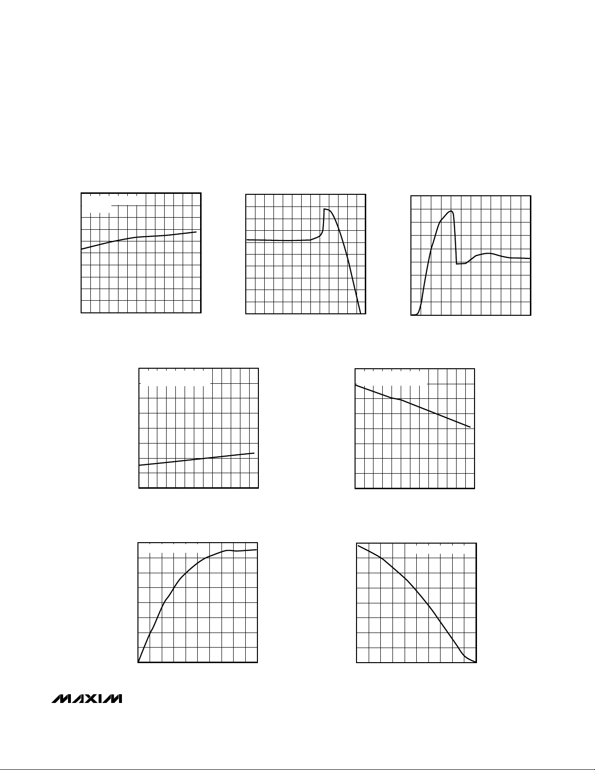
2.0
-40 20
DRIVER DIFFERENTIAL OUTPUT VOLTAGE
vs. TEMPERATURE
MAX3480EA/EB toc01
TEMPERATURE (°C)
DIFFERENTIAL OUTPUT VOLTAGE (V)
0-20 6040 80
2.1
2.2
2.3
2.4
2.5
2.6
2.7
2.8
2.9
3.0
DI´ = HIGH OR OPEN
R
L
= 54Ω
0
OUTPUT CURRENT
vs. DRIVER OUTPUT HIGH VOLTAGE
MAX3480EA/EB toc02
OUTPUT HIGH VOLTAGE (V)
OUTPUT CURRENT (mA)
0
-10
-20
-30
-40
-50
-60
-70
-80
-90
-100
-6 -4 -2 2 4 6
OUTPUT CURRENT
vs. DRIVER OUTPUT LOW VOLTAGE
MAX3480EA/EB toc03
OUTPUT LOW VOLTAGE (V)
OUTPUT CURRENT (mA)
0
160
180
140
100
120
80
40
60
0
20
24 681012
0
-40 20
RECEIVER OUTPUT LOW VOLTAGE
vs. TEMPERATURE
MAX3480EA/EB toc04
TEMPERATURE (°C)
OUTPUT LOW VOLTAGE (V)
0-20 6040 80
0.1
0.2
0.3
0.4
0.5
0.6
0.7
0.8
MEASURED AT ISO RO DRV
I
RO
= 8mA
TEMPERATURE (°C)
3.00
-40 20
RECEIVER OUTPUT HIGH VOLTAGE
vs. TEMPERATURE
MAX3480EA/EB toc05
OUTPUT HIGH VOLTAGE (V)
0-20 6040 80
3.25
3.50
3.75
4.00
4.25
4.50
4.75
5.00
MEASURED AT ISO RO DRV
I
RO
= 8mA
__________________________________________Typical Operating Characteristics
(V
CC_
= +3.3V, TA= +25°C, Figure 1, unless otherwise noted.)
0
OUTPUT CURRENT
vs. RECEIVER OUTPUT HIGH VOLTAGE
MAX3480EA/EB toc07
DIFFERENTIAL OUTPUT VOLTAGE (V)
OUTPUT CURRENT (mA)
10
20
30
40
50
60
70
80
1.00 3.02.0 5.04.0
MEASURED AT ISO RO DRV
0
OUTPUT CURRENT
vs. RECEIVER OUTPUT LOW VOLTAGE
MAX3480EA/EB toc06
OUTPUT LOW VOLTAGE (V)
OUTPUT CURRENT (mA)
10
20
30
40
50
60
70
80
MEASURED AT ISO RO DRV
1.003.02.0 5.04.0
Page 6

MAX3480EA/MAX3480EB
±15kV ESD-Protected, Isolated, 3.3V
RS-485/RS-422 Data Interfaces
6 _______________________________________________________________________________________
Typical Operating Characteristics (continued)
(V
CC_
= +3.3V, TA= +25°C, Figure 1, unless otherwise noted.)
0
0.5
1.5
1.0
2.0
2.5
-40 0-20 20 40 60 80
DRIVER ENABLE TIME
vs. TEMPERATURE
MAX3480EA/EB toc14
TEMPERATURE (°C)
DRIVER ENABLE TIME (µs)
RL = 54Ω, DI´ = 0
MEASURED FROM DE
´
TO VALID OUTPUT
MAX3480EB
MAX3480EA
350
0
MAX3480EA
SUPPLY CURRENT vs. SUPPLY VOLTAGE
300
250
MAX3480EA/EB toc10
SUPPLY VOLTAGE (V)
SUPPLY CURRENT (mA)
100
150
50
3.0 3.2 3.4 3.6 3.8
200
DE´ HIGH, 50Ω LOAD
DE
´
HIGH, 100Ω LOAD
DE´ LOW, DI´ LOW, RL =
∞
DE´ LOW, DI´ HIGH, RL =
∞
300
0
MAX3480EB
SUPPLY CURRENT vs. SUPPLY VOLTAGE
200
250
MAX3480EA/EB toc13
SUPPLY VOLTAGE (V)
SUPPLY CURRENT (mA)
100
50
3.0 3.2 3.63.4 3.8
150
DE´ HIGH,
100Ω LOAD
DE´ HIGH, 50Ω LOAD
DE´ LOW, DI´ LOW, RL = ∞
DE´ LOW, DI´ HIGH, RL = ∞
MAX3480EB DRIVER INPUT (AB)
AND RECEIVER OUTPUT (RO)
1µs/div
DI
´ INPUT,
2V/div
A
B
RO,
74HC240,
2V/div
2V/div
MAX3480EA/EB
toc11
MAX3480EA DRIVER INPUT (AB)
AND RECEIVER OUTPUT (RO)
CIRCUIT OF FIGURE 2, TERMINATION: 100Ω
100ns/div
DI
´ INPUT,
2V/div
A
B
RO,
74HC240,
2V/div
2V/div
MAX3480EA/EB
toc08
MAX3480EA DRIVER ENABLE (AB)
AND RECEIVER OUTPUT (RO)
MAX3480EA/EB
toc09
CIRCUIT OF FIGURE 2, TERMINATION: 100Ω
DE
´ INPUT,
1V/div
A, 1V/div
B, 2V/div
100ns/div
MAX3480EB DRIVER ENABLE (DE´)
AND DRIVER OUTPUT (AB)
MAX3480EA/EB
toc12
DE´
1V/div
A
2V/div
B
2V/div
20µs/div
0.5
1.5
1.0
2.0
DRIVER ENABLE TIME
vs. TEMPERATURE
MAX3480EA/EB TOC15
TEMPERATURE (°C)
DRIVER ENABLE TIME (µs)
-40 -20 0 20 40 60 80
MAX3480EA
MAX3480EB
RL = 54Ω, DI´ = 0V MEASURED FROM
DE
´ TO VALID OUTPUT
Page 7

MAX3480EA/MAX3480EB
±15kV ESD-Protected, Isolated, 3.3V
RS-485/RS-422 Data Interfaces
_______________________________________________________________________________________ 7
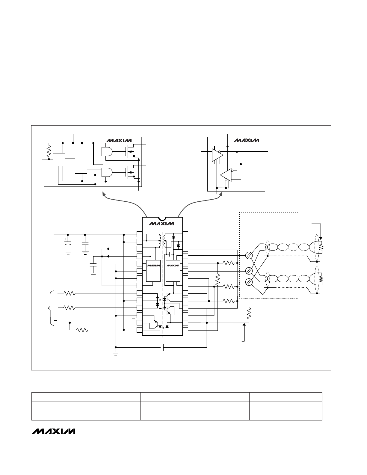
______________________________________________________________Pin Description
PIN NAME FUNCTION
PINS ON THE NONISOLATED SIDE
1V
CC1
Logic-Side (Nonisolated Side) +3.3V Supply Voltage Input. Connect to pins 2, 10, and 14.
2V
CC2
Logic-Side (Nonisolated Side) +3.3V Supply Voltage Input. Connect to pins 1, 10, and 14.
3, 4 D1, D2 Boost-Voltage Generator Outputs. See Figures 1 and 2.
5, 12
GND1,
GND2
Logic-Side Ground Inputs. Must be connected; not internally connected.
6FS
Frequency Switch Input. If V
FS
= VCC, switch frequency is high; if FS = 0, switch frequency is low
(normal connection).
7SDPower-Supply Shutdown Input. Must be connected to logic ground.
8V
CC3
Boosted V+ Voltage Input. Must be connected as shown in Figures 1 and 2.
9DI
Driver Input. With DE´ high, a low on DI´ forces output A low and output B high. Similarly, a high on
DI´ forces output A high and output B low. Drives internal LED cathode through R1 (Table 1).
10 V
CC4
Logic-Side (Nonisolated Side) +3.3V Supply Voltage Input. Connect to pins 1, 2, and 14.
11 DE
Driver-Enable Input. The driver outputs, A and B, are enabled by bringing DE´ high. The driver
outputs are high impedance when DE´ is low. If the driver outputs are enabled, the device functions
as a line driver. While the driver outputs are high impedance, the device functions as a line receiver.
Drives internal LED cathode through R2 (Table 1).
13 RO
Receiver Output. If A > B by 200mV, RO is low; if A < B by 200mV, RO is high. Open collector; must
have pullup (R3) to V
CC
(Table 1).
14 V
CC5
Logic-Side (Nonisolated Side) +3.3V Supply Voltage Input. Connect to pins 1, 2, and 10.
Page 8

MAX3480EA/MAX3480EB
±15kV ESD-Protected, Isolated, 3.3V
RS-485/RS-422 Data Interfaces
8 _______________________________________________________________________________________
Note: For DE´and DI´pin descriptions, see Detailed Block Diagram.
_________________________________________________Pin Description (continued)
PIN NAME FUNCTION
PINS ON THE ISOLATED RS-485/RS-422 SIDE
15
ISO RO
LED
Isolated Receiver-Output LED Anode (Input). If A > B by 200mV, ISO RO LED is high; if A < B by
200mV, ISO RO LED is low.
16
Isolated-Supply Common Input. Connect to ISO COM1.
17
ISO DE
DRV
Isolated Driver-Enable Drive Input. The driver outputs, A and B, are enabled by bringing DE´ high.
The driver outputs are high impedance when DE´ is low. If the driver outputs are enabled, the
device functions as a line driver. While the driver outputs are high impedance, the device functions
as a line receiver. Open collector output; must have pullup (R4 in Figure 1) to ISO VCC and be
connected to ISO DE IN for normal operation (Table 1).
18
Isolated-Supply Positive Input Voltage. Connect to ISO V
CC1
.
19
Isolated Driver-Input Drive. With DE´ high, a low on DI´ forces output A low and output B high.
Similarly, a high on DI´ forces output A high and output B low. Open-collector output; must have
pullup (R5 in Figure 1) to ISO VCC and be connected to ISO DI IN for normal operation (Table 1).
20
Isolated-Supply Common Output. Connect to ISO COM2. If RS-485 wires have a shield, connect
ISO COM1 to shield through 100Ω resistor.
21
Isolated Driver-Enable Input. Connect to ISO DE DRV for normal operation.
22
Isolated Driver Input. Connect to ISO DI DRV for normal operation.
23 A Noninverting Driver Output and Noninverting Receiver Input
24
Isolated Receiver-Output Drive. Connect to ISO RO LED through R6 (Table 1 and Figure 1).
25 B Inverting Driver Output and Inverting Receiver Input
26
Isolated Supply Positive Output Voltage. Connect to ISO V
CC2
.
27, 28
Internal Connections. Leave these pins unconnected.
ISO COM2
ISO V
CC2
ISO DI DRV
ISO COM1
ISO DE IN
ISO DI IN
ISO RO DRV
ISO V
CC1
AC2, AC1
Page 9
MAX3480EA/MAX3480EB
±15kV ESD-Protected, Isolated, 3.3V
RS-485/RS-422 Data Interfaces
_______________________________________________________________________________________ 9
_______________Detailed Description
The MAX3480EA/MAX3480EB are electrically isolated,
RS-485/RS-422 data-communications interface solutions. Transceivers, optocouplers, a power driver, and a
transformer are in one standard 28-pin PDIP package.
Signals and power are internally transported across the
isolation barrier (Figure 1). Power is transferred from the
logic side (nonisolated side) to the isolated side of the
barrier through a center-tapped transformer. Signals
cross the barrier through high-speed optocouplers. A
single +3.3V supply on the logic side powers both
sides of the interface.
Figure 1. Block Diagram
AC1 (MAKE NO CONNECTION)
AC2 (MAKE NO CONNECTION)
SHIELD (OPTIONAL)
EXTERNAL RS-485/RS-422 WIRING
ISO V
CC1
B
D2
D1
D1, D2
1N914
V
CC2
V
CC1
ISO RO DRV
A
B
A
SH
ISO DI IN
ISO DE IN
V
CC3
SD
FS
GND1
ISO COM1
ISO DI DRV
ISO V
CC2
ISO DE DRV
GND2
DE
V
CC4
DI
ISO COM2
ISO RO LED
V
CC5
RO
R
L
R
L
R4*
R5*
R8
100Ω
BOOSTED V+
C3
0.01µF
C4
270pF
4kV
R6*
R7*
R1*
R2*
DI
´
DE´
R3*
RO
LOGIC
I/O
V
IN
+3.0V TO +3.6V
C1
22µF
C2
0.1µF
MAX3480EA/EB
LOGIC GROUND
ISOLATION BARRIER
ISOLATION COMMON
MAX845
1
2
28
27
3
4
5
6
7
8
9
10
11
12
13
14
26
25
24
23
22
21
20
19
18
17
16
15
MAX845
N
MAX3480EA: MAX485E
MAX3480EB: MAX487E
RE
ISO RO DRV
ISO DE IN
ISO DI IN
ISO COM1
ISO V
CC1
A
B
R
D
N
Q
Q
TF/F
V
CC3
FS
OSC
1.1MHz/
1.6MHz
SD
GND1
D2
D1
SHIELD (OPTIONAL)
NOTE: RESISTOR R8 PROTECTS THE
MAX3480E FROM TRANSIENT
CURRENTS BETWEEN SHIELD AND
A AND B.
TWISTED PAIR
TO OTHER TRANSCEIVERS
TERMINATING RESISTOR
(ONE RESISTOR ON EACH END)
TWISTED PAIR
TO OTHER TRANSCEIVERS
MAX1487E
MAX487E
*SEE TABLE 1.
Table 1. Pullup and LED Drive Resistors
PART R1 (Ω) R2 (Ω) R3 (Ω) R4 (Ω) R5 (Ω) R6 (Ω)
MAX3480EA 100 100 680 3600 1000 200
MAX3480EB 100 100 2000 3600 3600 200
R7 (Ω)
Open
430
Page 10

MAX3480EA/MAX3480EB
±15kV ESD-Protected, Isolated, 3.3V
RS-485/RS-422 Data Interfaces
10 ______________________________________________________________________________________
The MAX3480EB features reduced-slew-rate drivers
that minimize EMI and reduce reflections caused by
improperly terminated cables, allowing error-free transmission at data rates up to 160kbps. The MAX3480EA’s
driver slew rates are not limited, allowing transmission
rates up to 2.5Mbps.
The frequency-select FS is connected to GND_ in normal
operation, which selects a switching frequency of
approximately 600kHz. Connect to high for a higher
900kHz switching frequency.
Drivers are short-circuit current limited and are protected against excessive power dissipation by thermal
shutdown circuitry that puts the driver outputs into a
high-impedance state. The receiver input has a fail-safe
feature that guarantees a logic-high output if the input
is open circuit.
The driver outputs are enabled by bringing DE´ high.
Driver-enable times are typically 500ns for the
MAX3480EA and 1µs for the MAX3480EB. Allow time
for the devices to be enabled before sending data.
When enabled, driver outputs function as line drivers.
Driver outputs are high impedance when DE´ is low.
While outputs are high impedance, they function as line
receivers.
Figure 2. Typical Application Circuit
AC1 (MAKE NO CONNECTION)
AC2 (MAKE NO CONNECTION)
SHIELD (OPTIONAL)
EXTERNAL RS-485/RS-422 WIRING
ISO V
CC1
B
D2
D1
D1, D2
1N914
V
CC2
V
CC1
ISO RO DRV
A
B
A
SH
ISO DI IN
ISO DE IN
V
CC3
SD
FS
GND1
ISO COM1
ISO DI DRV
ISO V
CC2
ISO DE DRV
GND2
DE
V
CC4
DI
ISO COM2
ISO RO LED
V
CC5
RO
R
L
R
L
R4*
R5*
R1*
R2*
16
14
12
5
7
13
15
18
3
8 2
DI
DE
RO
17
20
9
10
11 RECEIVER OUTPUT
6
4
R8
100Ω
C3
0.01µF
C4
270pF
4kV
R6*
R7*
R3*
BOOSTED V+
74HC240
DRIVER INPUT
DRIVER ENABLE
V
IN
+3.0V TO +3.6V
C1
22µF
6V
C2
0.1µF
MAX3480EA/EB
LOGIC GROUND
ISOLATION BARRIER
1
2
28
27
3
4
5
6
7
8
9
10
11
12
13
14
26
25
24
23
22
21
20
19
18
17
16
15
ISOLATION COMMON
SHIELD (OPTIONAL)
NOTE: RESISTOR R8 PROTECTS
THE MAX3480E FROM TRANSIENT
CURRENTS BETWEEN SHIELD AND
A AND B.
TWISTED PAIR
TO OTHER TRANSCEIVERS
TERMINATING RESISTOR
(ONE RESISTOR ON EACH END)
TWISTED PAIR
TO OTHER TRANSCEIVERS
MAX845
MAX1487E
MAX487E
*SEE TABLE 1.
Page 11

MAX3480EA/MAX3480EB
±15kV ESD-Protected, Isolated, 3.3V
RS-485/RS-422 Data Interfaces
______________________________________________________________________________________ 11
_________________________________________________________________Test Circuits
Figure 3. Driver DC Test Load Figure 4. Driver/Receiver Timing Test Circuit
Figure 5. Driver Timing Test Load
R
R
A
B
V
OD
V
OC
_______________________________________________________Switching Waveforms
Figure 6. Driver Propagation Delays and Transition Times Figure 7. Driver Enable and Disable Times
DI
´
VCC_ - 0.4V
V
CC
_ - 0.4V
2
VCC_ - 0.4V
2
0
B
A
V
O
0
-V
O
V
O
t
PLH
1/2 V
O
10%
t
R
90%
90%
t
PHL
1/2 V
O
10%
t
F
V
DIFF
= VA - V
B
V
DIFF
t
SKEW = | tPLH
- t
PHL
|
ISOLATION BARRIER ISOLATION BARRIER
+3.3V
DE
´
A
DI
´
V
ID
B
C
L1
R
DIFF
C
L2
ISO V
CC1,
ISO V
CC2
OUTPUT
UNDER TEST
500Ω
C
L
S1
S2
A
RD
B
+3.3V
R3
RO
VCC_ - 0.4V
DE
´
A, B
V
A, B
_ - 0.4V
V
CC
2
0
t
ZL
2.3V
OL
0
OUTPUT NORMALLY LOW
OUTPUT NORMALLY HIGH
2.3V
t
ZH
VCC_ - 0.4V
t
LZ
t
HZ
2
V
V
OL
OH
+ 0.5V
- 0.5V
Page 12

MAX3480EA/MAX3480EB
±15kV ESD-Protected, Isolated, 3.3V
RS-485/RS-422 Data Interfaces
12 ______________________________________________________________________________________
Figure 8. Receiver Propagation Delays
V
OH
V
OL
V
ID
-V
ID
1.5V
0
1.5V
OUTPUT
INPUT
0
RO
V
B
- V
A
t
PLH
t
PHL
t
SKD
= |t
PLH
- t
PHL
|
__Switching Waveforms (continued)
Function Tables
Table 2. Transmitting
INPUTS
DE´ DI´
B A
1 1 0 1
1 0 1 0
0 X
High
Impedance
High
Impedance
INPUTS OUTPUT
DE´
A-B
–R—O–
0 ≥ +0.2V 0
0 ≤ -0.2V 1
0 Inputs open 0
OUTPUTS
Table 3. Receiving
X = Don’t care.
The MAX3480EA/MAX3480EB withstand 1260V
RMS
(1 min) or 1560V
RMS
(1s). The isolated outputs of these
devices meet all RS-485/RS-422 specifications.
Boost Voltage
The MAX3480EA/MAX3480EB require external diodes
on the primary of the transformer to develop the boost
voltage for the power oscillator. In normal operation,
whenever one of the oscillator outputs (D1 and D2)
goes low, the other goes to approximately double the
supply voltage. Since the circuit is symmetrical, the two
outputs can be combined with diodes, filtered, and
used to power the oscillator itself.
The diodes on the primary side may be any fast-switching, small-signal diodes, such as the 1N914, 1N4148,
or CMPD2838. The nominal value of the primary filter
capacitor C3 is 0.01µF.
Driver Output Protection
There are two mechanisms to prevent excessive output
current and power dissipation caused by faults or by
bus contention. A foldback current limit on the output
stage provides immediate protection against short circuits over the whole common-mode voltage range (see
the Typical Operating Characteristics). In addition, a
thermal shutdown circuit forces the driver outputs into
a high-impedance state if the die temperature rises
excessively.
Resistor R8 (Figures 1 and 2) provides additional protection by current limiting between the shield and the
two signal wires. In the event that shielded cable is
used and an external voltage or transient is inadvertently applied between the shield and the signal wires,
the MAX3480EA/MAX3480EB can be damaged.
Although unlikely, this condition can occur during
installation.
The MAX3480EA/MAX3480EB provide electrical isolation between logic ground and signal paths; they
do not provide isolation from external shields and
the signal paths. When in doubt, do not connect the
shield. The MAX3480EA/MAX3480EB can be damaged if resistor R8 is shorted out.
Applications Information
The MAX3480EA/MAX3480EB provide extra protection
against ESD. The MAX3480EA/MAX3480EB are intended for harsh environments where high-speed communication is important. These devices eliminate the
need for transient suppressor diodes or the use of
discrete protection components. The standard (non-E)
MAX3480A/MAX3480B are recommended for applications where cost is critical.
Page 13

MAX3480EA/MAX3480EB
±15kV ESD-Protected, Isolated, 3.3V
RS-485/RS-422 Data Interfaces
______________________________________________________________________________________ 13
±15kV ESD Protection
As with all Maxim devices, ESD-protection structures
are incorporated on all pins to protect against electrostatic discharges encountered during handling and
assembly. The driver outputs and receiver inputs have
extra protection against static electricity. Maxim’s engineers developed state-of-the-art structures to protect
these pins against ESD of ±15kV without damage. The
ESD structures withstand high ESD in all states: normal
operation, shutdown, and power-down. After an ESD
event, Maxim’s MAX3480EA/MAX3480EB keep working
without latchup. An isolation capacitor of 270pF 4kV
should be placed between ISO COM and logic ground
for optimal performance against an ESD pulse with
respect to logic ground.
ESD protection can be tested in various ways; the
transmitter outputs and receiver inputs of this product
family are characterized for protection to ±15kV using
the Human Body Model.
ESD Test Conditions
The +15kV ESD test specifications apply only to the A, B,
Y, and Z I/O pins. The test surge may be referenced to
either the ISO COM or to the nonisolated GND (this presupposes that a bypass capacitor is installed between
V
CC2
and the nonisolated GND).
Human Body Model
Figure 9 shows the Human Body Model, and Figure 10
shows the current waveform it generates when discharged into a low impedance. This model consists of a
100pF capacitor charged to the ESD voltage of interest,
which is then discharged into the test device through a
1.5kΩ resistor.
Machine Model
The Machine Model for ESD tests all pins using a 200pF
storage capacitor and zero discharge resistance. Its
objective is to simulate the stress caused by contact that
occurs with handling and assembly during manufacturing. Of course, all pins require this protection during
manufacturing—not just inputs and outputs. Therefore,
after PC board assembly, the Machine Model is less relevant to l/O ports.
The MAX3480EA/MAX3480EB are designed for bidirectional data communications on multipoint bus-transmission lines. Figure 11 shows a typical network application
circuit. To minimize reflections, terminate the line at both
ends with its characteristic impedance, and keep stub
lengths off the main line as short as possible. The slewrate-limited MAX3480EB is more tolerant of imperfect termination and stubs off the main line.
The MAX3480EA/MAX3480EB are specified and characterized using the resistor values shown in Table 1.
Altering the recommended values can degrade performance.
The DI and DE inputs are the cathodes of LEDs whose
anodes are connected to VCC. These points are best
driven by a +3.3V CMOS-logic gate with a series
resistor to limit the current. The resistor values shown
in Table 1 are recommended when the 74HC240 gate
or equivalent is used. DI and DE are intended to be
CHARGE-CURRENT
LIMIT RESISTOR
DISCHARGE
RESISTANCE
STORAGE
CAPACITOR
C
s
100pF
R
C
1MΩ
R
D
1500Ω
HIGH-
VOLTAGE
DC
SOURCE
DEVICE
UNDER
TEST
Figure 9. Human Body ESD Test Model
IP 100%
90%
36.8%
t
RL
TIME
t
DL
CURRENT WAVEFORM
PEAK-TO-PEAK RINGING
(NOT DRAWN TO SCALE)
I
r
10%
0
0
AMPERES
Figure 10. Human Body Model Current Waveform
Page 14

MAX3480EA/MAX3480EB
driven through a series current-limiting resistor.
Directly grounding these pins destroys the device.
Reliability
These products contain transformers, optocouplers,
and capacitors, in addition to several monolithic ICs
and diodes. As such, the reliability expectations more
closely represent those of discrete optocouplers, rather
than the more robust characteristics of monolithic silicon ICs. The reliability testing programs for these multicomponent devices may be viewed on the Maxim
website (www.maxim-ic.com) under Technical Support,
Technical Reference, Multichip Products.
±15kV ESD-Protected, Isolated, 3.3V
RS-485/RS-422 Data Interfaces
14 ______________________________________________________________________________________
Table 4. Maxim’s ±15kV ESD-Protected Isolated RS-485 Product Family
PART
MAX1480EA 2.50
GUARANTEED
DATA RATE
(Mbps)
SLEW-RATE
LIMITED
No
SUPPLY
VOLTAGE
(V)
5.0
NO. OF
Tx/Rx
FULL/HALF
DUPLEX
NO. OF Tx/Rx
ON BUS
1/1 Half 128
MAX1480EC 0.25 Yes1/1 Half 5.0128
MAX1490EA 2.50 No1/1 Full 5.032
MAX1490EB 0.25 Yes1/1 Full 5.032
MAX3480EA 2.50 No1/1 Half 3.3128
MAX3480EB 0.25 Yes1/1 Half 3.3128
Page 15

MAX3480EA/MAX3480EB
±15kV ESD-Protected, Isolated, 3.3V
RS-485/RS-422 Data Interfaces
______________________________________________________________________________________ 15
Figure 11. Typical RS-485/RS-422 Network
DI
DE
RO
BA
R
D
RE
RO
DE
DI
R
120
Ω
D
A
B
RERE
DI
DE
RO
BA
R
D
AC1 (MAKE NO CONNECTION)
AC2 (MAKE NO CONNECTION)
SHIELD
(OPTIONAL)
ISO V
CC1
B
D2
D1
V
CC2
V
CC1
ISO RO DRV
A
B
A
SH
ISO DI IN
ISO DE IN
V
CC3
SD
FS
GND1
ISO COM1
ISO DI DRV
ISO V
CC2
ISO DE DRV
DE
GND2
V
CC4
DI
ISO COM2
ISO RO LED
V
CC5
RO
R4*
R7*
R5*
R8
100
Ω
120Ω
R6*
MAX3480EA/EB
LOGIC GROUND
*SEE TABLE 1.
ISOLATION BARRIER
TERMINATING RESISTOR
(ONE RESISTOR ON EACH END)
MAX845
MAX1487E
MAX487E
1
2
28
27
3
4
5
6
7
8
9
10
11
12
13
14
26
25
24
23
22
21
20
19
18
17
16
15
TERMINATING RESISTOR
(ONE RESISTOR ON EACH END)
D1, D2
1N914
R1*
R2*
R3*
BOOSTED V+
DRIVER INPUT
DRIVER ENABLE
V
IN
+3.0V TO +3.6V
C1
22µF
6V
C2
0.1µF
C3
0.01µF
C4
270pF
4kV
16
14
12
5
7
13
15
8 2
DI
DE
RO
17
20
18
3
9
10
11
RECEIVER OUTPUT
6
4
74HC240
NOTE: RESISTOR R8
PROTECTS THE MAX3480E
FROM TRANSIENT
CURRENTS BETWEEN
SHIELD AND A AND B.
ISOLATION
COMMON
Page 16

MAX3480EA/MAX3480EB
±15kV ESD-Protected, Isolated, 3.3V
RS-485/RS-422 Data Interfaces
Maxim cannot assume responsibility for use of any circuitry other than circuitry entirely embodied in a Maxim product. No circuit patent licenses are
implied. Maxim reserves the right to change the circuitry and specifications without notice at any time.
16 ____________________Maxim Integrated Products, 120 San Gabriel Drive, Sunnyvale, CA 94086 408-737-7600
© 2006 Maxim Integrated Products is a registered trademark of Maxim Integrated Products, Inc.
PDIPW.EPS
PACKAGE OUTLINE, .600" PDIP
1
1
21-0044
B
REV.DOCUMENT CONTROL NO.APPROVAL
PROPRIETARY INFORMATION
TITLE:
TOP VIEW
FRONT VIEW
0.700
MAX
-
0.200
0.020
0.080
0.009
0.625
0.012
0.065
0.600 BSC
INCHES
E1
-
eA
eB
0.005
0.600
0.008
D1
E
C
DIM
0.045
0.016
0.055
0.015
B
B1
A1
A3
MIN
-A
15.24 BSC
-
0.13
0.21
15.24
17.78
0.22
15.87
0.30
MILLIMETERS
0.39
0.41
1.40
1.14
-
MIN
0.51
1.65
-
2.03
MAX
5.08
A2
0.125 0.175 3.18 4.45
0.525 0.575 13.34 14.61
e
0.100 BSC 2.54 BSC
0.150
0.120L
3.05 3.81
2.0752.025D
D
MINDIM
D
INCHES
MAX
51.44 52.71
MILLIMETERS
MIN
MAX
40
AC
1.430 1.470 AB37.3436.32 28
1.230 1.270 AA32.2631.24 24
N MS011
N
D
A
L
A1
e
B
B1
A2
A3
E1
E
C
eA
eB
0∞-15∞
SIDE VIEW
1
D1
VARIATIONS:
Package Information
(The package drawing(s) in this data sheet may not reflect the most current specifications. For the latest package outline information,
go to www.maxim-ic.com/packages
.)
 Loading...