19-0453; Rev 0; 1/96
Complete, Isolated, 3.3V
RS-485/RS-422 Data Interface
_______________General Description
The MAX3480A/MAX3480B are electrically isolated
RS-485/RS-422 data-communications interfaces.
Transceivers, optocouplers, and a transformer are all
included in one low-cost, 28-pin DIP package. A single
+3.3V supply on the logic side powers both sides of the
interface.
The MAX3480B features reduced-slew-rate drivers that
minimize EMI and reduce reflections caused by
improperly terminated cables, allowing error-free data
transmission at data rates up to 250kbps. The
MAX3480A’s driver slew rate is not limited, allowing
transmission rates up to 2.5Mbps.
These devices typically draw 180mA of quiescent supply current. The MAX3480B provides a low-power shutdown mode in which it consumes only 0.2µA.
Drivers are short-circuit current limited and are protected against excessive power dissipation by thermal
shutdown circuitry that places the driver outputs into a
high-impedance state. The receiver input has a fail-safe
feature that guarantees a logic-high output if the input
is open circuit.
The MAX3480A/MAX3480B typically withstand 1600V
(1 minute) or 2000V
(1 second). Their isolated inputs
RMS
RMS
and outputs meet RS-485/RS-422 specifications.
________________________Applications
Isolated RS-485/RS-422 Data Interface
Transceivers for EMI-Sensitive Applications
Industrial-Control Local Area Networks
Automatic Test Equipment
HVAC/Building Control Networks
______________Ordering Information
DATA
PART
MAX3480ACPI
MAX3480AEPI
MAX3480BCPI
MAX3480BEPI -40°C to +85°C 28 Plastic DIP
TEMP. RANGE PIN-PACKAGE
0°C to +70°C
-40°C to +85°C
0°C to +70°C
28 Plastic DIP
28 Plastic DIP
28 Plastic DIP
RATE
(kbps)
2500
2500
250
250
____________________________Features
♦ Isolated Data Interface to 1600V
♦ Slew-Rate-Limited Data Transmission (MAX3480B)
♦ High-Speed, Isolated, 2.5Mbps RS-485 Interface
(MAX3480A)
♦ -7V to +12V Common-Mode Input Voltage Range
with Respect to Isolated Ground
♦ Single +3.3V Supply
♦ Current Limiting and Thermal Shutdown for
Driver Overload Protection
♦ Standard 28-Pin DIP Package
RMS
(1 minute)
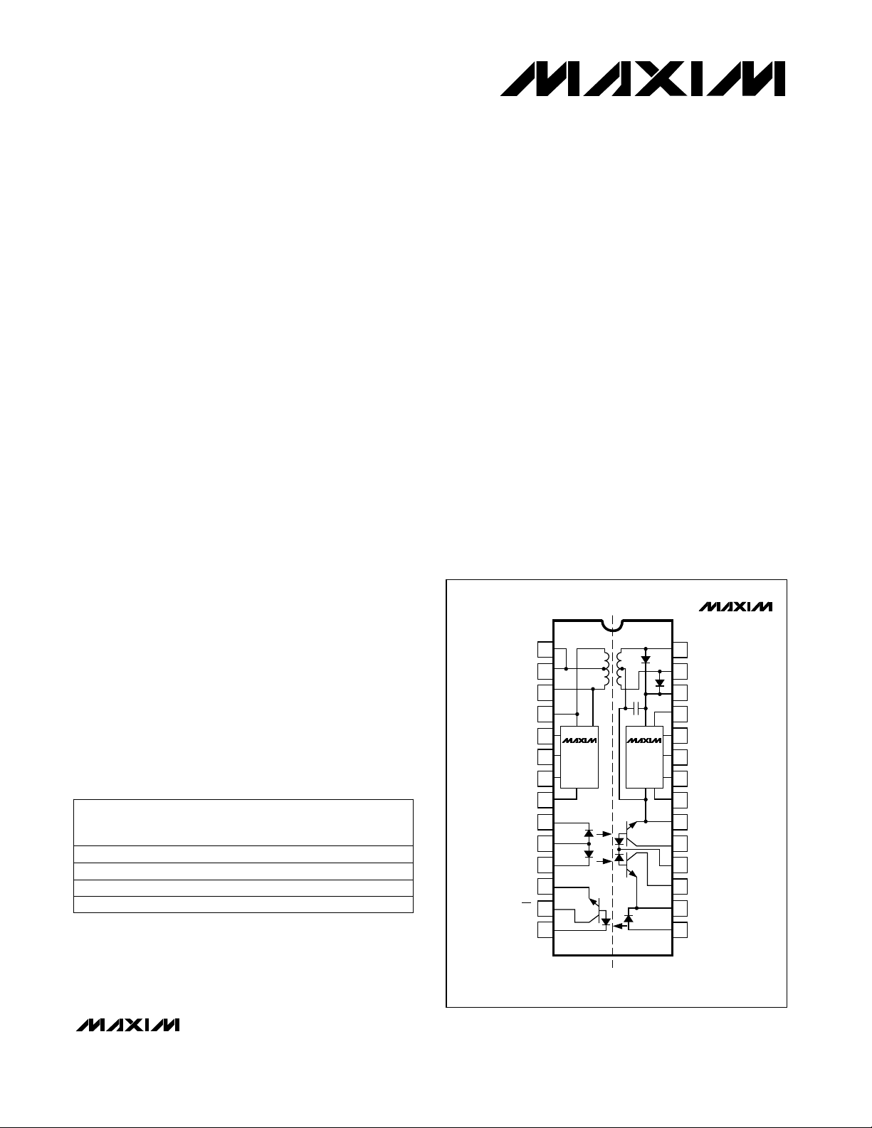
__________________Pin Configuration
TOP VIEW
MAX3480A/B
V
CC1
V
CC2
GND1
CC3
V
CC4
GND2
V
CC5
1
2
D1
3
D2
4
5
MAX845
6
FS
SD
7
8
DI
9
10
DE
11
12
RO
13
14
MAX485
MAX487
28
27
26
25
24
23
22
21
20
19
18
17
16
15
AC1
AC2
ISO V
CC1
B
ISO RO DRV
A
ISO DI IN
ISO DE INV
ISO COM1
ISO DI DRV
ISO V
CC2
ISO DE DRV
ISO COM2
ISO RO LED
MAX3480A/MAX3480B
ISOLATION BARRIER
DIP
________________________________________________________________
Maxim Integrated Products
1
For free samples & the latest literature: http://www.maxim-ic.com, or phone 1-800-998-8800

Complete, Isolated, 3.3V
RS-485/RS-422 Data Interface
ABSOLUTE MAXIMUM RATINGS
With Respect to GND:
V
V
V
Supply Voltage (V
Supply Voltage (V
CC
CC
2,
CC
1,
) ..........................................-0.3V to +7V
CC3
Control Input Voltage (SD, FS)................-0.3V to (V
Receiver Output Voltage (RO
).................-0.3V to (VCC+ 0.3V)
).........-0.3V to +3.8V
CC
4,
5
CC
+ 0.3V)
With Respect to ISO COM:
Control Input Voltage (ISO DE _) .........-0.3V to (ISO V
Driver Input Voltage (ISO DI _).........-0.3V to (ISO V
Receiver Output Voltage (ISO RO _)......-0.3V to (ISO V
CC
CC
CC
+ 0.3V)
+ 0.3V)
+ 0.3V)
Driver Output Voltage (A, B)................................-8V to +12.5V
Receiver Input Voltage (A, B)..............................-8V to +12.5V
Stresses beyond those listed under “Absolute Maximum Ratings” may cause permanent damage to the device. These are stress ratings only, and functional
operation of the device at these or any other conditions beyond those indicated in the operational sections of the specifications is not implied. Exposure to
absolute maximum rating conditions for extended periods may affect device reliability.
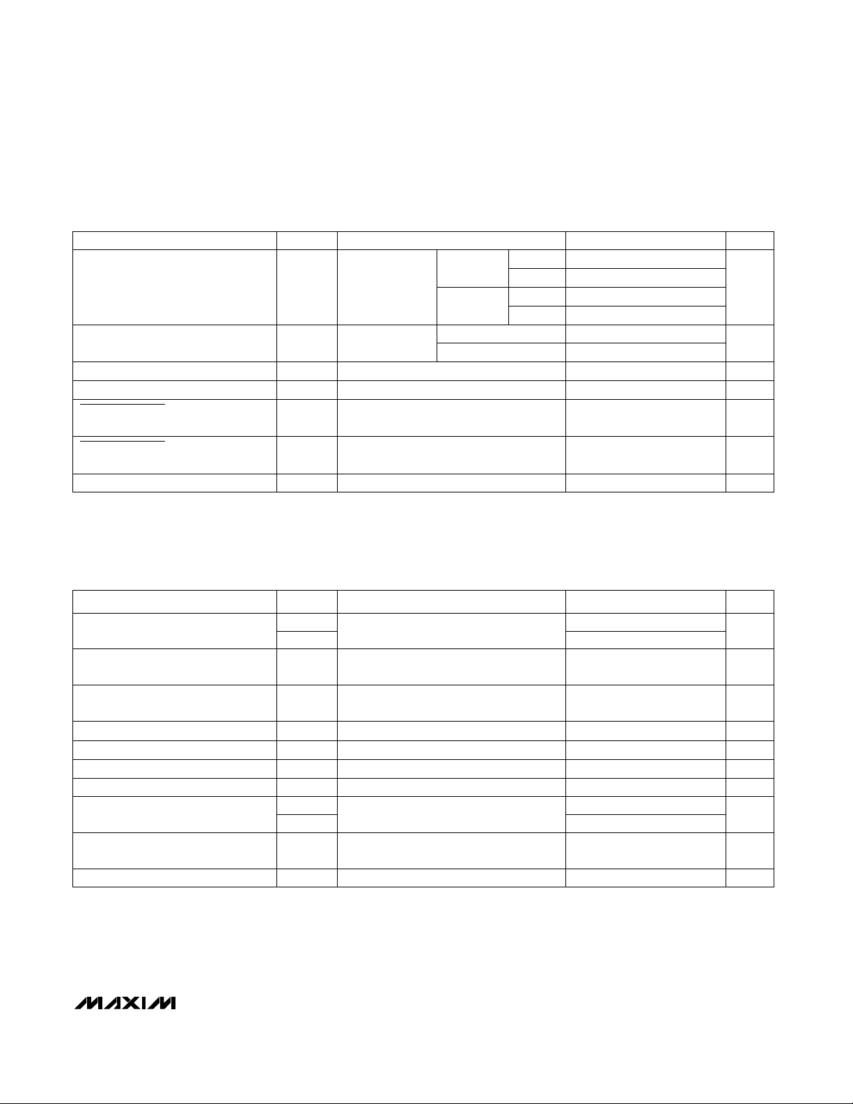
ELECTRICAL CHARACTERISTICS
(VCC= V
= V
V
CC
MAX3480A/MAX3480B
Switch Frequency
Operating Supply Current
FS Input Threshold
FS Input Pull-Up Current
FS Input Leakage Current
Input High Voltage
Input Low Voltage
Isolation Resistance
Isolation Capacitance
Differential Driver Output (no load) V
Differential Driver Output (with load)
CC1
CC1
= V
= V
CC2
CC2
= V
= V
CC4
CC4
= V
= 3.0V to 3.6V, FS = 0V, TA= T
CC5
= V
= 3.3V and TA= +25°C.) (Notes 1, 2, 3)
CC5
V
S
f
SWL
f
SWH
FS = 0V
FS = VCCor open
MAX3480A,
= VCCor open
DE
I
CC
I
SHDN
FSH
FSL
FSL
FSM
ISO
ISO
V
OD1
IH
IL
´
MAX3480B,
= V
DE
´
SD = V
High
Low
FS low
FS high
DE´, DI´(Figure 1)
DE´, DI´(Figure 1)
TA= +25°C, V
TA= +25°C, V
R = 50Ω (RS-422)
V
OD2
R = 27Ω (RS-485), Figure 3 1.5 5
CC
CC3
LED Forward Current (DI, DE, ISO RO LED) ......................50mA
Continuous Power Dissipation (TA= +70°C)
Plastic DIP (derate 9.09mW/°C above +70°C)...............727mW
Operating Temperature Ranges
MAX3480_CPI......................................................0°C to +70°C
MAX3480_EPI...................................................-40°C to +85°C
Storage Temperature Range.............................-65°C to +160°C
Lead Temperature (soldering, 10sec).............................+300°C
to T
MIN
, unless otherwise noted. Typical values are at
MAX
CONDITIONS
3.0 3.3 3.6Supply Voltage
600
900
180 260
280
120 200
240
or open
RL= ∞
RL= 54Ω
RL= ∞
RL= 54Ω
2.4V
0.8V
- 0.4V
CC
= 50V
ISO
ISO
= 50V
DC
DC
8
2
UNITSMIN TYP MAXSYMBOLPARAMETER
V
kHz
mA
µAShutdown Supply Current (Note 3) 0.2
V
µA50I
pA10I
VV
V0.4V
MΩ100 10,000R
pF10C
V
Change in Magnitude of Driver
Output Voltage for Complementary
Output States
Driver Common-Mode Output V
∆V
R = 27Ω or 50Ω,
OD
Figure 3
R = 27Ω or 50Ω, Figure 4
OC
Differential
2 _______________________________________________________________________________________
0.3
0.3Common Mode
4
V
V

Complete, Isolated, 3.3V
RS-485/RS-422 Data Interface
ELECTRICAL CHARACTERISTICS (continued)
(VCC= V
= V
V
CC
Input Current (A, B)
Receiver Input Hysteresis
Receiver Output/Receiver Output
Low Voltage
Receiver Output/Receiver Output
High Current
Driver Short-Circuit Current
CC1
CC1
= V
= V
CC2
CC2
= V
= V
CC4
CC4
= V
= 3.0V to 3.6V, FS = 0V, TA= T
CC5
= V
= 3.3V and TA= +25°C.) (Notes 1, 2, 3)
CC5
IN
IN
TH
TH
OL
OSD
DE´= 0V,
= 0V or 3.6V
V
CC
-7V ≤ VCM≤ 12V
-7V ≤ VCM≤ 12V -0.2 0.2V
VCM= 0V
DI´= V
V
= 3.6V, DI´= 0V
OUT
-7V ≤ VO≤ 12V (Note 4) mA100ISO I
ISO I
R
OH
CONDITIONS
CC
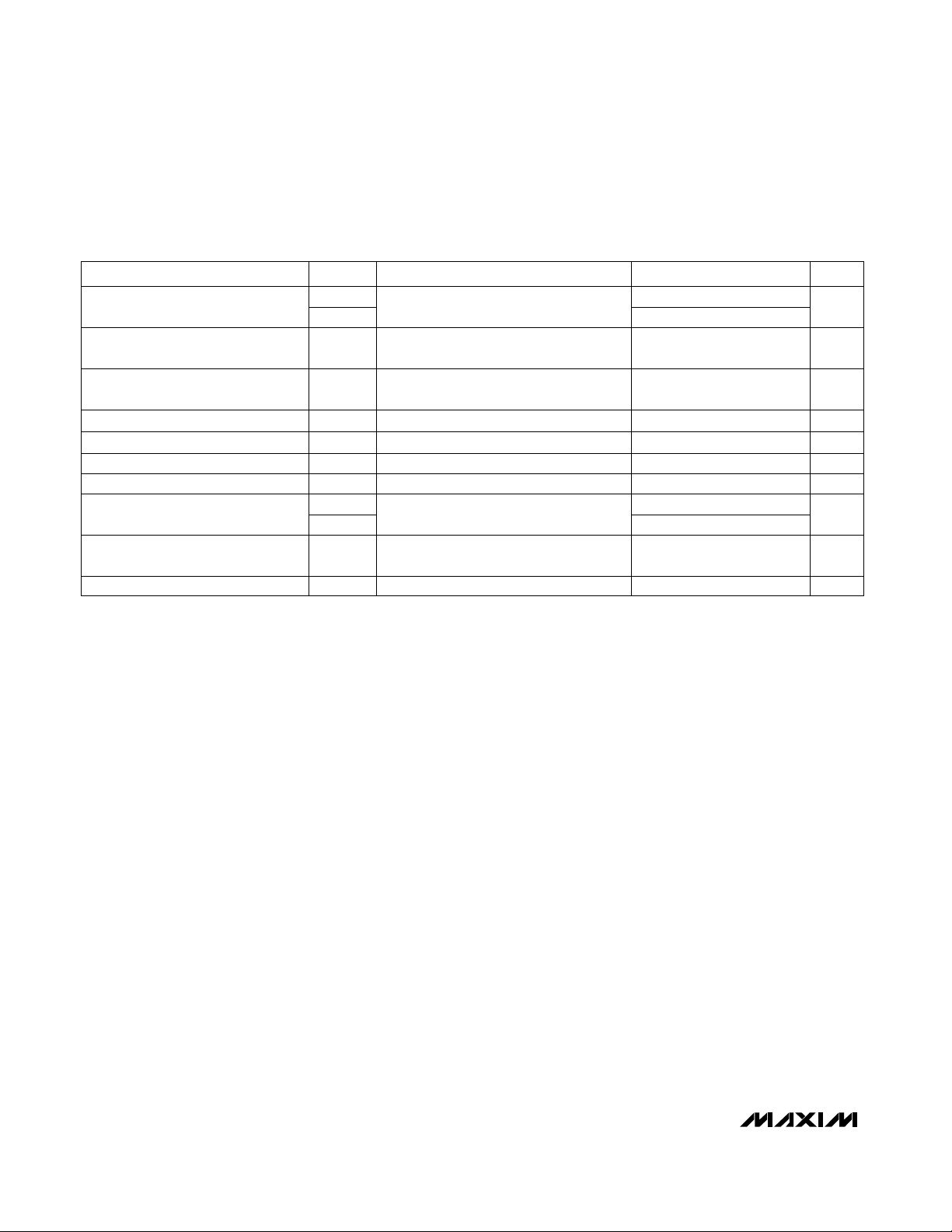
SWITCHING CHARACTERISTICS—MAX3480A
(VCC= V
= V
V
CC
Driver Input to Output
Propagation Delay
Driver Output Skew (Note 5)
Driver Rise or Fall Time
Driver Enable to Output High
Driver Enable to Output Low
Driver Disable Time from High
Driver Disable Time from Low
Receiver Input to Output
Propagation Delay
t
PLH - tPHL
Receiver Skew
Maximum Data Rate
= V
CC1
= V
CC1
PARAMETER SYMBOL MIN TYP MAX UNITS
CC2
= V
CC2
Differential
= V
CC4 =VCC5
= V
CC4
= 3.0V to 3.6V, FS = 0V, TA= T
= 3.3V and TA= +25°C.)
CC5
t
PLH 100 275
t
PHL 100 275
t
SKEW 25 90 ns
tR, t
t
ZH 0.2 1.5 µs
t
t
HZ 0.3 1.5 µs
t
t
PLH
t
PHL
t
SKD
f
MAX 2.5 Mbps
Figures 4, 6; R
CL1= CL2= 100pF
Figures 4, 6; R
CL1= CL2= 100pF
Figures 4, 6; R
F 15 40 ns
CL1= CL2= 100pF
Figures 5, 7; CL= 100pF, S2 closed
ZL 0.2 1.5 µs
Figures 5, 7; CL= 100pF, S1 closed
Figures 5, 7; CL= 15pF, S2 closed
LZ 0.3 1.5 µsFigures 5, 7; C
Figures 4, 8; R
CL1= CL2= 100pF
Figures 4, 8; R
CL1= CL2= 100pF
t
PLH, tPHL < 50% of data period
CONDITIONS
DIFF
DIFF
DIFF
L
DIFF
DIFF
to T
MIN
MAX3480A
MAX3480B
MAX3480A
, unless otherwise noted. Typical values are at
MAX
VIN= 12V
VIN= 12V
VIN= -7V
VIN= 12V
VIN= -7V
12
MAX3480B 48
MIN
to T
, unless otherwise noted. Typical values are at
MAX
= 54Ω,
= 54Ω,
= 54Ω,
= 15pF, S1 closed
= 54Ω,
= 54Ω,
1.0
0.8
-0.8
0.25
-0.2
70∆V
100 225
100 225
20
MAX3480A/MAX3480B
UNITSMIN TYP MAXSYMBOLPARAMETER
mA
kΩReceiver Input Resistance
VReceiver Differential Threshold
mV
V0.4V
µA250I
ns
ns
ns
_______________________________________________________________________________________ 3

Complete, Isolated, 3.3V
RS-485/RS-422 Data Interface
SWITCHING CHARACTERISTICS—MAX3480B
(VCC= V
= V
V
CC
Driver Input to Output
Propagation Delay
Driver Output Skew t
Driver Rise or Fall Time tR, t
Driver Enable to Output High t
Driver Enable to Output Low t
Driver Disable Time from Low t
Driver Disable Time from High t
Receiver Input to Output
Propagation Delay
t
PLH
MAX3480A/MAX3480B
Receiver Skew
Maximum Data Rate f
Note 1: All currents into device pins are positive; all currents out of device pins are negative. All voltages are referenced to
Note 2: For DE
Note 3: Shutdown supply current is the current at V
Note 4: Applies to peak current. See
= V
CC1
= V
CC1
PARAMETER SYMBOL MIN TYP MAX UNITS
- t
PHL
logic-side ground (GND1, GND2), unless otherwise specified.
MAX3480A/MAX3480B).
= V
CC2
CC2
Differential
and DI´pin descriptions, see
´
= V
CC4
CC4 =VCC5
= V
= 3.0V to 3.6V, FS = 0V, TA= T
= 3.3V and TA= +25°C.)
CC5
Typical Operating Characteristics
t
PLH
t
PHL
SKEW
ZH
HZ
t
PLH
t
PHL
t
SKD
MAX
Figures 4, 6; R
CL1= CL2= 100pF
Figures 4, 6; R
CL1= CL2= 100pF
Figures 4, 6; R
F
CL1= CL2= 100pF
Figures 5, 7; CL= 100pF, S2 closed
Figures 5, 7; CL= 100pF, S1 closed
ZL
Figures 5, 7; CL= 15pF, S1 closed
LZ
Figures 4, 8; R
CL1= CL2= 100pF
Figures 4, 8; R
CL1= CL2= 100pF
, t
PLH
PHL
Detailed Block Diagram
when shutdown is enabled.
CC1
to T
MIN
CONDITIONS
= 54Ω,
DIFF
= 54Ω,
DIFF
= 54Ω,
DIFF
= 54Ω,
DIFF
= 54Ω,
DIFF
< 50% of data period
and
and
MAX
Typical Application Circuit
Applications Information
, unless otherwise noted. Typical values are at
1.0 2.0
1.0 2.0
100 800 ns
1.0 2.0 µs
50 100 µs
50 100 µs
13 50 µs
13 50 µsFigures 5, 7; CL= 15pF, S2 closed
0.8 2.0
0.8 2.0
50
0.25 Mbpst
(Figure 1 for
.
µs
µs
ns
4 _______________________________________________________________________________________

Complete, Isolated, 3.3V
RS-485/RS-422 Data Interface
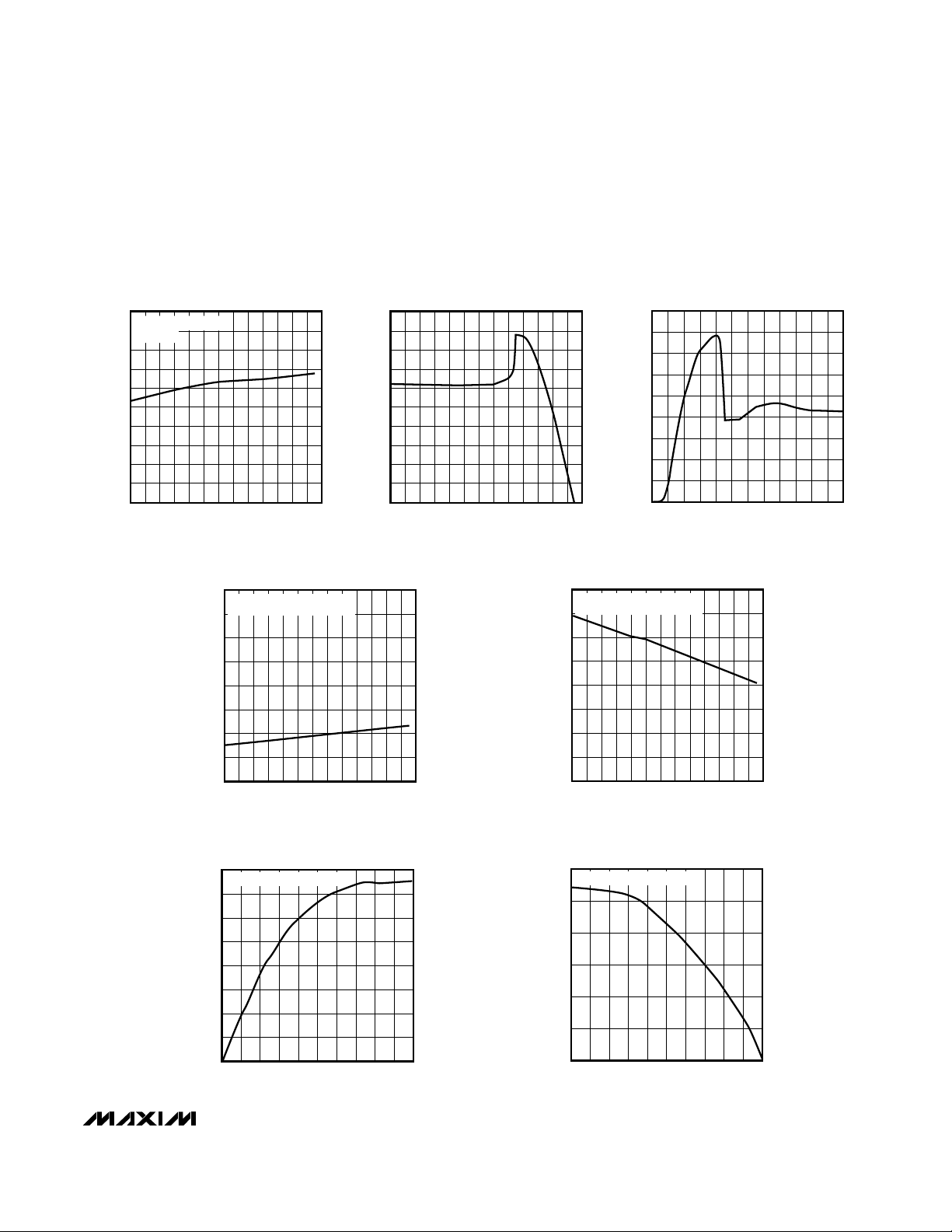
__________________________________________Typical Operating Characteristics
(V
= 3.3V, TA= +25°C, unless otherwise noted.)
CC_
DRIVER DIFFERENTIAL OUTPUT VOLTAGE
vs. TEMPERATURE
3.0
DI´ = HIGH OR OPEN
2.9
= 54Ω
R
L
2.8
2.7
2.6
2.5
2.4
2.3
2.2
DIFFERENTIAL OUTPUT VOLTAGE (V)
2.1
2.0
-40 20
0-20 6040 80
TEMPERATURE (°C)
RECEIVER OUTPUT LOW VOLTAGE
0.8
MEASURED AT ISO RO DRV
I
= 8mA
RO
0.7
0.6
0.5
0.4
0.3
0.2
OUTPUT LOW VOLTAGE (V)
0.1
0
-40 20
vs. DRIVER OUTPUT HIGH VOLTAGE
-100
-90
MAX3480A/B-08
-80
-70
-60
-50
-40
-30
OUTPUT CURRENT (mA)
-20
-10
0
-6 -4 -2 2 4 6
vs. TEMPERATURE
0-20 6040 80
TEMPERATURE (°C)
OUTPUT CURRENT
0
OUTPUT HIGH VOLTAGE (V)
MAX3480 A/B-04
180
160
MAX3480 A/B-06
140
120
100
80
60
OUTPUT CURRENT (mA)
40
20
0
0
RECEIVER OUTPUT HIGH VOLTAGE
vs. TEMPERATURE
5.00
MEASURED AT ISO RO DRV
I
= 8mA
RO
4.75
4.50
4.25
4.00
3.75
3.50
OUTPUT HIGH VOLTAGE (V)
3.25
3.00
-40 20
0-20 6040 80
TEMPERATURE (°C)
OUTPUT CURRENT
vs. DRIVER OUTPUT LOW VOLTAGE
24681012
OUTPUT LOW VOLTAGE (V)
MAX3480 A/B-03
MAX3480A/MAX3480B
MAX3480 A/B-05
vs. RECEIVER OUTPUT LOW VOLTAGE
OUTPUT CURRENT
80
MEASURED AT ISO RO DRV
70
60
50
40
30
OUTPUT CURRENT (mA)
20
10
0
1.00 3.02.0 5.04.0
OUTPUT LOW VOLTAGE (V)
MAX3480 A/B-01
vs. RECEIVER OUTPUT HIGH VOLTAGE
-30
-25
-20
-15
-10
OUTPUT CURRENT (mA)
-5
0
OUTPUT CURRENT
MEASURED AT ISO RO DRV
MAX3480 A/B-02
1.00 3.02.0 5.04.0
OUTPUT HIGH VOLTAGE (V)
_______________________________________________________________________________________
5
 Loading...