For free samples & the latest literature: http://www.maxim-ic.com, or phone 1-800-998-8800.
For small orders, phone 408-737-7600 ext. 3468.
________________General Description
The MAX3471 half-duplex transceiver is intended for
lithium battery-powered RS-485/RS-422 applications. It
draws only 1.6µA (typical) supply current from a 3.6V
supply with the receiver enabled and the driver disabled. Its wide 2.5V to 5.5V supply voltage guarantees
operation over the lifetime of a lithium battery.
This device features true fail-safe operation that guarantees a logic-high receiver output when the receiver
inputs are open or shorted. This means that the receiver output will be a logic high if all transmitters on a terminated bus are disabled (high impedance). The
MAX3471 has a 1/8-unit load input resistance. When
driver outputs are enabled and pulled above VCCor
below GND, internal circuitry prevents battery backcharging.
The MAX3471 is available in an 8-pin µMAX package.
________________________Applications
Remote Meter Reading
Battery-Powered Differential Communications
Level Translators
____________________________Features
♦ 1.6µA Supply Current with Receiver Enabled
♦ +2.5V to +5.5V Single-Supply Operation
♦ True Fail-Safe Receiver Input
♦ Available in µMAX Package
♦ 1/8-Unit-Load Receiver Input
♦ -7V to +10V Common-Mode Input Voltage Range
MAX3471
1.6µA, RS-485/RS-422, Half-Duplex,
Differ ential T ransceiver for Battery-Powered Systems
________________________________________________________________
Maxim Integrated Products
1
1
2
3
4
8
7
6
5
V
CC
B
A
GNDDI
DE
RE
RO
MAX3471
µMAX
TOP VIEW
___________________Pin Configuration
MAX3471
B
A
B
A
R
DI
V
CC
V
CC
GND
GND
REMOTE UNIT
DE
RO
D
RE
R
DE
DI
RO
D
RE
R
DI DE
D
BA
RERO
TYPICAL HALF-DUPLEX RS-485 NETWORK
R
DI DE
D
BA
RERO
V
CC
GND
V
CC
V
CC
0.1µF
CENTRAL UNIT
REMOTE UNIT
REMOTE UNIT
19-0497; Rev 0; 2/98
PART
MAX3471CUA
MAX3471EUA -40°C to +85°C
0°C to +70°C
TEMP. RANGE PIN-PACKAGE
8 µMAX
8 µMAX
_______________Ordering Information
Typical Application Circuit

MAX3471
1.6µA, RS-485/RS-422, Half-Duplex,
Differ ential T ransceiver for Battery-Powered Systems
2 _______________________________________________________________________________________
ABSOLUTE MAXIMUM RATINGS (Note 1)
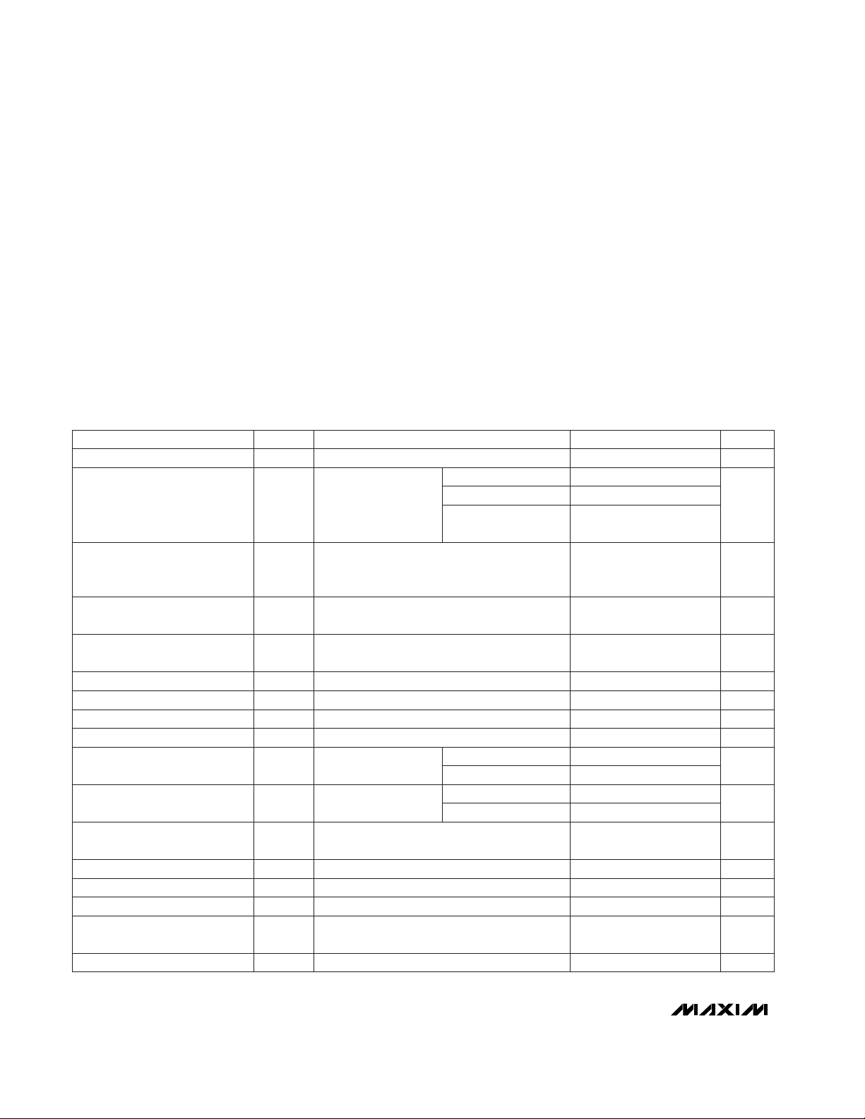
DC ELECTRICAL CHARACTERISTICS
(VCC= +2.5V to +5.5V, TA= T
MIN
to T
MAX
, unless otherwise noted. Typical values are at VCC= +3.6V and TA= +25°C.) (Note 1)
Stresses beyond those listed under “Absolute Maximum Ratings” may cause permanent damage to the device. These are stress ratings only, and functional
operation of the device at these or any other conditions beyond those indicated in the operational sections of the specifications is not implied. Exposure to
absolute maximum rating conditions for extended periods may affect device reliability.
Supply Voltage (VCC) ..............................................................7V
Control Input Voltage (
RE, DE)...................-0.3V to (VCC+ 0.3V)
Driver Input Voltage (DI).............................-0.3V to (V
CC
+ 0.3V)
Driver Output/Receiver Input Voltage (A, B).....................±10.5V
Receiver Output Voltage (RO)....................-0.3V to (V
CC
+ 0.3V)
Continuous Power Dissipation
µMAX (derate 4.5mW/°C above +70°C) ......................362mW
Operating Temperature Ranges
MAX3471CUA.....................................................0°C to +70°C
MAX3471EUA..................................................-40°C to +85°C
Storage Temperature Range.............................-65°C to +160°C
Lead Temperature (soldering, 10sec).............................+300°C
VIN= 10V
VIN= -7V -0.075
V
CC
≤ 5.5V
Figure 1
-130 130
Figure 1 (R = open)
IO = 2.2mA, VID= -450mV
IO = -0.8mA, VID= -50mV
V
CM
= 0
DE, DI, RE
-7V ≤ VCM≤ 10V
V
CC
≤ 3.6V
DE, DI, RE
Figure 1, R = 750Ω or 27Ω
Figure 1, R = 750Ω or 27Ω
DE = GND,
VCC= GND or 5.5V
Figure 1, R = 750Ω or 27Ω
DE, DI, RE
CONDITIONS
V0.4V
OL
Receiver Output Low Voltage
VVCC- 0.4V
OH
Receiver Output High Voltage
mV32∆V
TH
Receiver Input Hysteresis
mV-450 -250 -50V
TH
Receiver Differential Threshold
Voltage
mA
-60 60
I
OSD
Driver Short-Circuit Output
Current (Note 3)
mA
0.105
I
IN2
Input Current (A and B),
Half Duplex
µA±0.001 ±1I
IN1
Input Current
0.2 0.83
V
1.5 3.28
V
OD2
VV
CC
V
OD1
Differential Driver Output (no load)
Differential Driver Output
(with load)
mV100V
HYS
DI Input Hysteresis
V0.3 x V
CC
V
IL
Input Low Voltage
V0.7 x V
CC
V
IH
Input High Voltage
V0.2∆V
OC
Change in Magnitude of
Common-Mode Voltage (Note 2)
1.5
V0.2∆V
OD
Change in Magnitude of
Differential Output Voltage
(Note 2)
V0.6 x V
CC
V
OC
Driver Common-Mode Output
Voltage
UNITSMIN TYP MAXSYMBOLPARAMETER
R = 750Ω (RS-422)
R = 27Ω (RS-485)
R = 27Ω (RS-485),
V
CC
= 5V, TA= +25°C
0 ≤ VO≤ V
CC
µA±1I
OZR
Three-State Current at Receiver
Output
-7V ≤ VCM≤ 10V
kΩ
96R
IN
Receiver Input Resistance
-7V ≤ V
OUT
≤ 10V
Note 1: All currents into the device are positive; all currents out of the device are negative. All voltages are referred to device
ground unless otherwise noted.

MAX3471
1.6µA, RS-485/RS-422, Half-Duplex,
Differ ential T ransceiver for Battery-Powered Systems
_______________________________________________________________________________________ 3
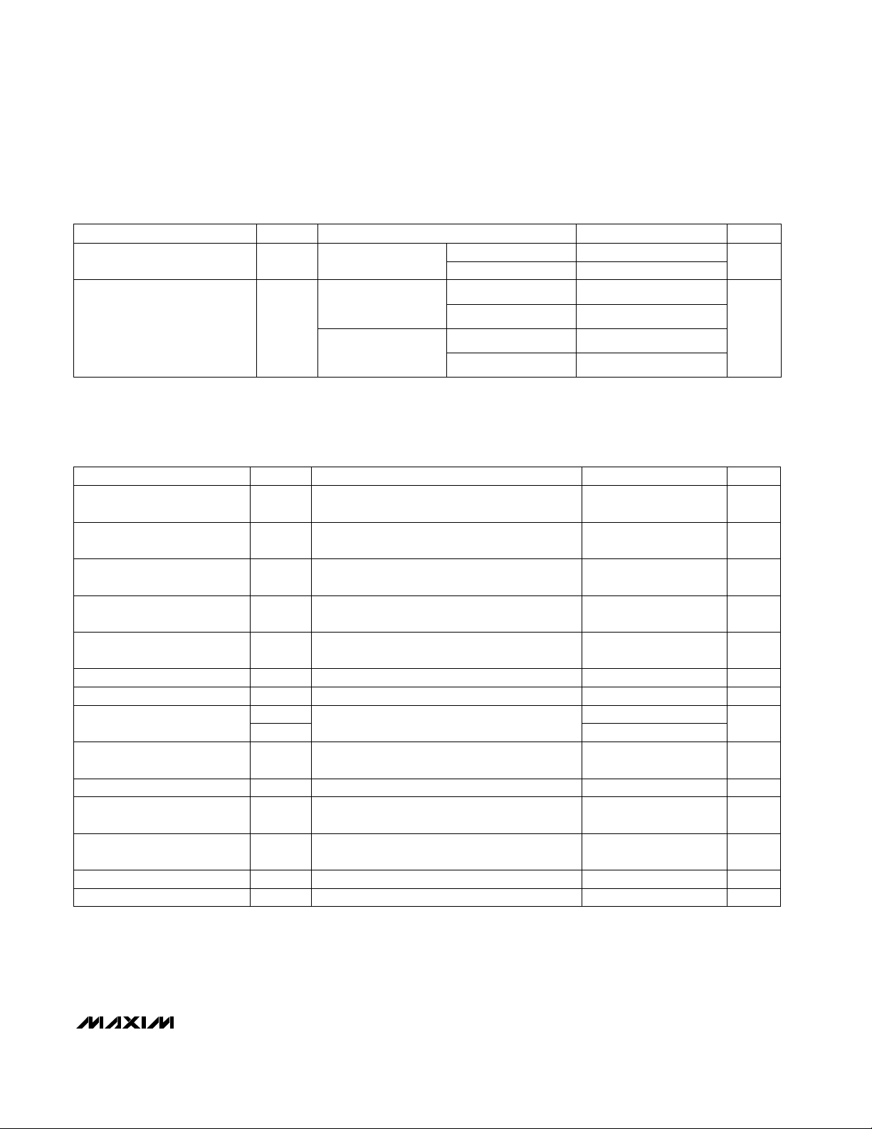
DC ELECTRICAL CHARACTERISTICS (continued)
(VCC= +2.5V to +5.5V, TA= T
MIN
to T
MAX
, unless otherwise noted. Typical values are at VCC= +3.6V and TA= +25°C.) (Note 1)
SWITCHING CHARACTERISTICS
(VCC= +2.5V to +5.5V, TA= T
MIN
to T
MAX
, unless otherwise noted. Typical values are at VCC= +3.6V and TA= +25°C.)
Note 1: All currents into the device are positive; all currents out of the device are negative. All voltages are referred to device
ground unless otherwise noted.
Note 2: ∆V
OD
and ∆VOCare the changes in magnitude of VODand VOC, respectively, when the DI input changes state.
Note 3: Maximum and minimum current levels apply to peak current just prior to foldback-current limiting.
0 ≤ VRO≤ V
CC
CONDITIONS
-20 50
UNITSMIN TYP MAXSYMBOLPARAMETER
V
CC
≤ 3.6V
mAI
OSR
Receiver Output Short-Circuit
Current
Figures 3 and 5, R
DIFF
= 1.5kΩ,
C
L1
= CL2= 100pF
Figures 3 and 5, R
DIFF
= 1.5kΩ,
C
L1
= CL2= 100pF
CONDITIONS
µs0.025t
DSKEW
Driver Output Skew
(t
DPLH
- t
DPHL
)
µs
Driver Input to Output
Propagation Delay
UNITSMIN TYP MAXSYMBOLPARAMETER
t
DPLH,
t
DPHL
1.40 2.00
Figures 3 and 5, R
DIFF
= 1.5kΩ,
C
L1
= CL2= 100pF
µs0.75 1.34 1.75tDR, t
DF
Driver Rise or Fall Time
Figures 4 and 6, CL= 100pF, S2 closed, S1 open µs1.5 6.00t
DZH
Driver Enable Time to Output
High
Figures 4 and 6, CL= 100pF, S1 closed, S2 open µs0.86 4.00t
DZL
Driver Enable Time to Output
Low
Figures 4 and 6, CL= 15pF, S1 closed, S2 open µs0.4 1.5t
DLZ
Driver Disable Time from Low
Figures 4 and 6, CL= 15pF, S2 closed, S1 open µs0.6 1.5t
DHZ
Driver Disable Time from High
Figures 7 and 9, CL= 15pF, |V
ID
|
= 2V
µs
6.4 12t
RPHL
Receiver Input to Output
Propagation Delay
Figures 7 and 9, |V
ID
|
= 2V
µs1.2t
RSKEW
Differential Receiver Skew
(t
RPLH
- t
RPHL
)
Figure 9, CL= 100pF kbps64f
MAX
Data Rate
Figures 2 and 8, CL= 15pF, S2 closed, S1 open ns85 500t
RZH
Receiver Enable Time to
Output High
Figures 2 and 8, CL= 15pF, S1 closed, S2 open ns50 200t
RLZ
Receiver Disable Time from Low
Figures 2 and 8, CL= 15pF, S2 closed, S1 open ns35 200t
RHZ
Receiver DisableTime from High
V
CC
≤ 5.5V -40 110
DE = V
CC
µAI
CC
Supply Current
V
CC
≤ 3.6V, no load,
RE = DI = GND or V
CC
,
V
A
= VB= 0
50 60
DE = GND 1.6 2
DE = V
CC
V
CC
≤ 5.5V, no load,
RE = DI = GND or V
CC
,
V
A
= VB= 0
83 100
DE = GND 2.8 4
Figures 2 and 8, CL= 15pF, S1 closed, S2 open ns70 500t
RZL
Receiver Enable Time to
Output Low
t
RPLH
5.2 12
 Loading...