

Page 1
General Description
The MAX3453E–MAX3456E ±15kV ESD-protected USBcompliant transceivers interface low-voltage ASICs with
USB devices. The devices fully comply with USB 1.1
and USB 2.0 when operating at full (12Mbps) and low
(1.5Mbps) speeds. The MAX3453E–MAX3456E operate
with VLas low as +1.65V, ensuring compatibility with
low-voltage ASICs.
The MAX3453E–MAX3456E feature a logic-selectable
suspend mode that reduces current consumption to
less than 40µA. Integrated ±15kV ESD protection protects the USB D+ and D- bidirectional bus connections.
The MAX3453E supports only full-speed (12Mbps)
operation. The MAX3453E/MAX3454E feature an internal 1.5kΩ USB pullup resistor and an enumeration function that allows devices to logically disconnect while
plugged in. The MAX3453E/MAX3455E provide a pushpull bus-detect (BD) output that asserts high when
V
BUS
> +4.0V.
The MAX3453E–MAX3456E operate over the extended
temperature range (-40°C to +85°C) and are available
in 14-pin TSSOP and 16-pin (3mm x 3mm) thin QFN
packages.
Applications
PDAs
PC Peripherals
Cellular Telephones
Data Cradles
MP3 Players
Features
♦ ±15kV ESD Protection on D+ and D-
♦ USB 1.1 and USB 2.0 (Low-Speed and Full-Speed)-
Compliant Transceivers
♦ Combined VP and VM Inputs/Outputs
♦ +1.65V to +3.6V V
L
Logic Supply Input for
Interfacing with Low-Voltage ASICs
♦ Enumerate Input Function (MAX3453E/MAX3454E)
♦ Powered from Li+ Battery as Low as +3.1V
(MAX3454E/MAX3456E)
♦ V
BUS
Detection (MAX3453E/MAX3455E)
♦ Internal Pullup Resistor (MAX3453E/MAX3454E)
♦ No Power-Supply Sequencing Required
MAX3453E–MAX3456E
±15kV ESD-Protected USB Transceivers
________________________________________________________________ Maxim Integrated Products 1
19-2924; Rev 4; 2/06
For pricing, delivery, and ordering information, please contact Maxim/Dallas Direct! at
1-888-629-4642, or visit Maxim’s website at www.maxim-ic.com.
Ordering Information
PART
PIN-PKG
PKG CODE
MAX3453EEUD
14 TSSOP U14-1
MAX3453EETE
T1633-4
MAX3454EEUD
14 TSSOP U14-1
MAX3454EETE
T1633-4
MAX3455EEUD
14 TSSOP U14-1
MAX3455EETE
T1633-4
MAX3456EEUD
14 TSSOP U14-1
MAX3456EETE
T1633-4
Typical Operating Circuit appears at end of data sheet.
Pin Configurations appear at end of data sheet.
Selector Guide
PART
V
BUS
POWER-
SUPPLY
VL POWER-
SUPPLY
INTERNAL
PULLUP
RESISTOR
V
BUS
LEVEL
DETECT
ENUMERATE
USB SPEED
±15kV ESD
PROTECTION
4.0 to 5.5 1.65 to 3.6 Yes Yes Yes Full Yes
3.0 to 5.5 1.65 to 3.6 Yes No Yes Low/full Yes
4.0 to 5.5 1.65 to 3.6 No Yes No Low/full Yes
3.0 to 5.5 1.65 to 3.6 No No No Low/full Yes
TEMP RANGE
-40oC to +85oC
-40oC to +85oC 16 Thin QFN
-40oC to +85oC
-40oC to +85oC 16 Thin QFN
-40oC to +85oC
-40oC to +85oC 16 Thin QFN
-40oC to +85oC
-40oC to +85oC 16 Thin QFN
VOLTAGE (V)
MAX3453E
MAX3454E
MAX3455E
MAX3456E
VOLTAGE (V)
SUPPORTED
Page 2
MAX3453E–MAX3456E
±15kV ESD-Protected USB Transceivers
2 _______________________________________________________________________________________
ABSOLUTE MAXIMUM RATINGS
Stresses beyond those listed under “Absolute Maximum Ratings” may cause permanent damage to the device. These are stress ratings only, and functional
operation of the device at these or any other conditions beyond those indicated in the operational sections of the specifications is not implied. Exposure to
absolute maximum rating conditions for extended periods may affect device reliability.
DC ELECTRICAL CHARACTERISTICS
(V
BUS
= +4.0V to +5.5V or V
TRM
= +3.0V to +3.6V, VL= +1.65V to +3.6V, TA= T
MIN
to T
MAX
, unless otherwise noted. Typical values
are at V
BUS
= +5.0V, VL= +2.5V, and TA= +25°C.) (Note 1)
PARAMETER
SYM B O L
CONDITIONS
MIN
TYP
MAX
UNITS
SUPPLY INPUTS (V
BUS
, V
TRM
, VL)
V
TRM
Internal regulator 3.0 3.3 3.6 V
Operating Supply Current I
VBUS
Full-speed transmitting and receiving at
10 mA
Operating VL Supply Current I
VL
Full-speed transmitting and receiving at
12Mbps (Note 2)
2.5 mA
Full-speed idle: VD+ > 2.7V, VD- < 0.3V
350
Full-Speed Idle and SE0 Supply
Current
)
SE0: VD+ < 0.3V, VD- < 0.3V
350
µA
15
Static VL Supply Current
)
Full-speed idle,
SE0, or suspend
mode
5
µA
MAX3453E
(ENUM = low),
MAX3455E
40
Suspend Supply Current
)
VM = VP = open,
MAX3454E
(ENUM = low),
MAX3456E
35
µA
Disable Mode Supply Current
)
VL = GND or open 20 µA
20
)
V
BUS
= GND or
open, OE = low,
VP = low or high,
VM = low or
5
µA
D+/D- Sharing Mode Load
Current
)
V
BUS
= GND or open, VD_ = 0 or +5.5V 20 µA
D+/D- Disable Mode Load
Current
I
D_(DIS)
VL = GND or open, VD_ = 0 or +5.5V 5 µA
V
BUS
, VL, D+, D- to GND.......................................-0.3V to +6.0V
V
TRM
to GND ............................................-0.3V to (V
BUS
+ 0.3V)
VP, VM, SUS, ENUM, SPD,
RCV,
OE, BD to GND ................................-0.3V to (VL+ 0.3V)
Current (into any pin) ........................................................±15mA
Short-Circuit Current (D+ and D-)...................................±150mA
Continuous Power Dissipation (T
A
= +70°C)
14-Pin TSSOP (derate 9.1mW/°C above +70°C) .........727mW
16-Pin Thin QFN (derate 14.7mW/°C above +70°C)....1176mW
Operating Temperature Range ...........................-40°C to +85°C
Junction Temperature......................................................+150°C
Storage Temperature Range .............................-65°C to +150°C
Lead Temperature (soldering, 10s) .................................+300°C
Regulated Supply Voltage Output
I
Sharing Mode VL Supply Current I
VBUS(IDLE
I
VL(STATIC
I
VBUS(SUSP
I
VBUS(DIS
VL(SHARING
I
D_(SHARING
12Mbps, CL = 50pF on D+ and D- (Note 2)
250
250
MAX3453E/MAX3455E
MAX3454E/MAX3456E
SUS = OE = high
high, SUS = high
MAX3453E/MAX3455E
MAX3454E/MAX3456E
Page 3
MAX3453E–MAX3456E
±15kV ESD-Protected USB Transceivers
_______________________________________________________________________________________ 3
DC ELECTRICAL CHARACTERISTICS (continued)
(V
BUS
= +4.0V to +5.5V or V
TRM
= +3.0V to +3.6V, VL= +1.65V to +3.6V, TA= T
MIN
to T
MAX
, unless otherwise noted. Typical values
are at V
BUS
= +5.0V, VL= +2.5V, and TA= +25°C.) (Note 1)
PARAMETER
CONDITIONS
UNITS
MAX3453E/MAX3455E, supply lost 3.6
MAX3453E/MAX3455E, supply present 4.0
MAX3454E/MAX3456E, supply lost 0.8
USB Power-Supply Detection
Threshold
MAX3454E/MAX3456E, supply present
(Note 3)
3.6
V
MAX3453E/MAX3455E 40
USB Power-Supply Detection
Hysteresis
MAX3454E/MAX3456E 75
mV
VL Power-Supply Detection
Threshold
V
TH_VL
V
DIGITAL INPUTS/OUTPUTS (VP, VM, RCV, SUS, OE, SPD, BD, ENUM)
Input-Voltage Low V
IL
VM, VP, SUS, SPD, ENUM, OE
V
Input-Voltage High V
IH
VM, VP, SUS, SPD, ENUM, OE
V
Output-Voltage Low V
OL
VM, VP, RCV, BD, IOL = +2mA 0.4 V
Output-Voltage High V
OH
VM, VP, RCV, BD, IOH = -2mA
V
Input Leakage Current I
LKG
-1 +1 µA
Input Capacitance C
IN
Measured from input to GND 10 pF
ANALOG INPUTS/OUTPUTS (D+, D-)
Differential Input Sensitivity V
ID
|VD+ - VD-| 0.2 V
Differential Common-Mode
Voltage
V
CM
Includes VID range 0.8 2.5 V
V
ILSE
0.8 V
V
IHSE
2.0 V
Hysteresis V
HYST
mV
Output-Voltage Low V
OLD
RL = 1.5kΩ to +3.6V 0.3 V
Output-Voltage High V
OHD
RL = 15kΩ to GND 2.8 3.6 V
Off-State Leakage Current I
LZ
-1 +1 µA
Transceiver Capacitance C
IND
Measured from D_ to GND 20 pF
Driver Output Impedance Z
DRV
Steady-state drive 3.5
Ω
Input Impedance Z
IN
Driver off 10 MΩ
Internal Pullup Resistance
I
LOAD
= 500µA (MAX3453E/MAX3454E)
(Note 4)
kΩ
ESD PROTECTION (D+, D-)
Human Body Model
kV
±8kV
Single-Ended Input Low Voltage
Single-Ended Input High Voltage
IEC 61000-4-2 Contact Discharge
SYM B O L
V
TH_VBUS
V
HYST_VBUS
R
PULLUP
MIN TYP MAX
0.7 x V
VL - 0.4
1.425 1.575
0.85
L
250
±15
0.3 x V
L
15.5
Page 4

MAX3453E–MAX3456E
±15kV ESD-Protected USB Transceivers
4 _______________________________________________________________________________________
Note 1: Parameters are 100% production tested at +25°C, unless otherwise noted. Limits over temperature are guaranteed by design.
Note 2: Guaranteed by design, not production tested.
Note 3: Production tested to +2.7V for VL< +3.0V.
Note 4: Including external 27Ω series resistor.
TIMING CHARACTERISTICS
(V
BUS
= +4.0V to +5.5V or V
TRM
= +3.0V to +3.6V, VL= +1.65V to +3.6V, TA= T
MIN
to T
MAX
, unless otherwise noted. Typical values
are at V
BUS
= +5V, VL= +2.5V, and TA= +25°C.) (Note 1)
PARAMETER
SYMBOL
CONDITIONS
MIN
TYP
MAX
UNITS
DRIVER CHARACTERISTICS (Full-Speed Mode, CL = 50pF)
Rise Time t
FR
10% to 90% of |V
OHD
- V
OLD
|, Figures 1, 6 4 20 ns
Fall Time t
FF
90% to 10% of |V
OHD
- V
OLD
|, Figures 1, 6 4 20 ns
Rise/Fall-Time Matching (Note 2)
Excluding the first transition from idle state,
Figures 1, 6
90 110 %
Output-Signal Crossover Voltage
(Note 2)
V
CRS_F
Excluding the first transition from idle state,
Figures 2, 6
1.3 2.0 V
Low-to-high transition, Figures 2, 6 18
Driver Propagation Delay
High-to-low transition, Figures 2, 6 18
ns
High-to-off transition, Figure 3 20 ns
Driver Disable Delay
Low-to-off transition, Figure 3 20 ns
Off-to-high transition, Figure 3 20 ns
Driver Enable Delay
Off-to-low transition, Figure 3 20 ns
DRIVER CHARACTERISTICS (low-speed mode, CL = 200pF to 600pF, MAX3454E/MAX3455E/MAX3456E)
Rise Time t
LR
10% to 90% of |V
OHD
- V
OLD
|, Figures 1, 6 75 300 ns
Fall Time t
LF
90% to 10% of |V
OHD
- V
OLD
|, Figures 1, 6 75 300 ns
Rise/Fall-Time Matching
Excluding the first transition from idle state,
Figures 1, 6
80 125 %
Output-Signal Crossover Voltage
V
CRS_L
Excluding the first transition from idle state,
Figures 2, 6
1.3 2.0 V
RECEIVER CHARACTERISTICS (CL = 15pF)
Low-to-high transition, Figures 4, 6 22
Differential Receiver Propagation
Delay
High-to-low transition, Figures 4, 6 22
ns
Low-to-high transition, Figures 4, 6 12
Single-Ended Receiver
Propagation Delay
High-to-low transition, Figures 4, 6 12
ns
High-to-off transition, Figure 5 15
Single-Ended Receiver Disable
Delay
t
PLZ_SE
Low-to-off transition, Figure 5 15
ns
Off-to-high transition, Figure 5 15
Single-Ended Receiver Enable
Delay
t
PZL_SE
Off-to-low transition, Figure 5 15
ns
tFR / t
FF
t
PLH_DRV
t
PHL_DRV
t
PHZ_DRV
t
PLZ_DRV
t
PZH_DRV
t
PZL_DRV
tLR / t
t
PLH_RCV
t
PHL_RCV
t
PLH_SE
t
PHL_SE
t
PHZ_SE
t
PZH_SE
LF
Page 5
MAX3453E–MAX3456E
±15kV ESD-Protected USB Transceivers
_______________________________________________________________________________________ 5
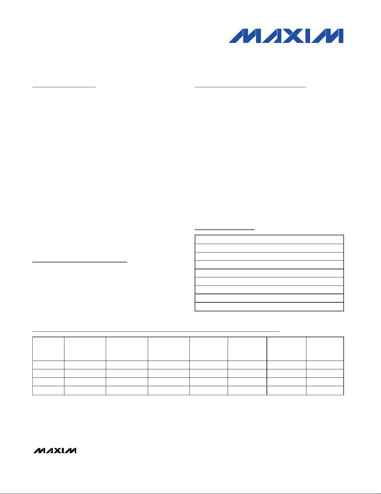
SINGLE-ENDED RECEIVER
PROPAGATION DELAY vs. V
L
MAX3453E-56E toc01
VL (V)
PROPAGATION DELAY (ns)
3.43.21.8 2.0 2.2 2.6 2.82.4 3.0
1
2
3
4
5
6
7
8
0
1.6 3.6
CL = 15pF
TA = +25°C
TA = +85°C
TA = -40°C
RISE-/FALL-TIME MATCHING
(FULL SPEED)
MAX3453E-56E toc02
20ns/div
D+/D1V/div
CL = 50pF
MAX3453E-56E toc03
100ns/div
RISE-/FALL-TIME MATCHING
(LOW SPEED)
CL = 400pF
D+/D1V/div
Typical Operating Characteristics
(V
BUS
= +5.0V, VL= +3.3V, TA= +25°C, unless otherwise noted.)
MAX3453E-56E toc04
20ns/div
OE, VP, VM TIMING
CL = 15pF
VP
2V/div
VM
2V/div
OE
5V/div
SUPPLY CURRENT
vs. D+/D- CAPACITANCE
MAX3453E-56E toc05
D+/D- CAPACITANCE (pF)
SUPPLY CURRENT (mA)
350300200 250100 15050
2
4
6
8
10
12
14
16
18
20
22
24
0
0 400
SPD = GND, fIN = 750kHz
SPD = VL, fIN = 6MHz
LOGIC SUPPLY CURRENT
vs. D+/D- CAPACITANCE
MAX3453E-56E toc06
D+/D- CAPACITANCE (pF)
LOGIC SUPPLY CURRENT (µA)
350300200 250100 15050
50
100
150
200
250
300
350
400
450
500
0
0400
SPD = GND, fIN = 750kHz
SPD = VL, fIN = 6MHz
Page 6
MAX3453E–MAX3456E
±15kV ESD-Protected USB Transceivers
6 _______________________________________________________________________________________
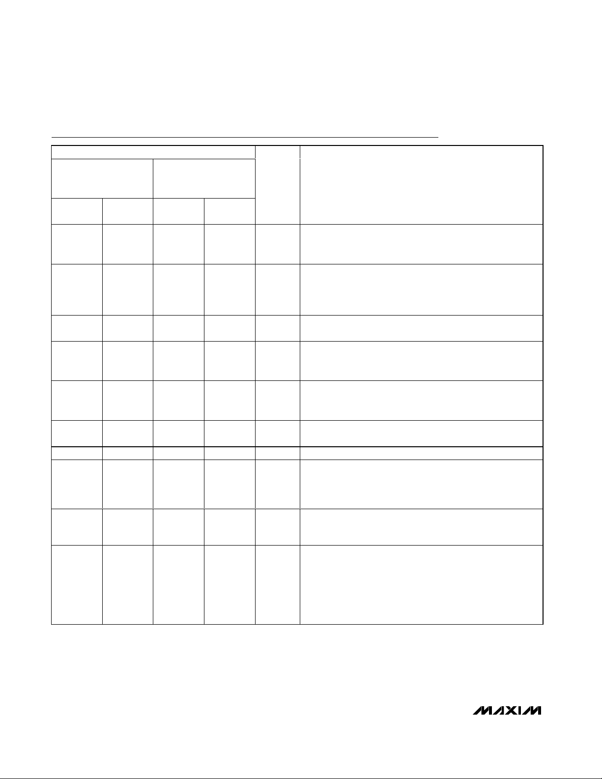
PIN
MAX3454E/
MAX3455E/
MAX3456E
MAX3453E
TSSOP
TSSOP
NAME
FUNCTION
1 15 1 15 V
L
Digital I/O Connections Logic Supply. Connect a +1.65V to
+3.6V supply to V
L
. Bypass VL to GND with a 0.1µF ceramic
capacitor.
21——SPD
Speed Selector Input. Connect SPD to GND to select the lowspeed data rate (1.5Mbps). Connect SPD to V
L
to select the fullspeed data rate (12Mbps). The MAX3453E only supports fullspeed operation.
3232RCV
D i ffer enti al Recei ver O utp ut. RC V r esp ond s to the d i ffer enti al i np uts
on D + and D - ( see Tab l es 3, 4) . RC V asser ts l ow i f S U S = V
L
.
4343VP
Receiver Output/Driver Input. VP functions as a receiver output
when OE = VL. VP duplicates D+ when receiving. VP functions
as a driver input when OE = GND.
5454VM
Receiver Output/Driver Input. VM functions as a receiver output
when OE = V
L
. VM duplicates D- when receiving. VM functions
as a driver input when OE = GND.
6, 13*
6 5, 8, 16 N.C.
No Connection. Not internally connected.
*Pin 13 is No Connection for MAX3456E only.
7676GNDGround
8787SUS
Suspend Input. Drive SUS low for normal operation. Drive SUS
high to put the MAX3453E–MAX3456E into suspend mode. RCV
asserts low in suspend mode. VP and VM remain active in
suspend mode.
9999OE
Output Enable. Drive OE to GND to enable the transmitter
outputs. Drive OE to V
L
to disable the transmitter outputs. OE
also controls the I/O direction of VP and VM (see Tables 3, 4).
10 10 10 10 D-
USB Input/Output. For OE = GND, D- functions as a USB
output, with VM providing the input signal. For OE = V
L
, Dfunctions as a USB input, with VM functioning as a single-ended
receiver output. Connect a 1.5kΩ resistor from D- to V
TRM
for
low-speed (1.5Mbps) operation (MAX3455E/MAX3456E). Drive
ENUM to V
L
to connect the internal 1.5kΩ resistor from D- to
V
TRM
for low-speed (MAX3454E, SPD = GND) operation.
Pin Description
THIN QFN
5, 8, 13*, 16
THIN QFN
Page 7

MAX3453E–MAX3456E
±15kV ESD-Protected USB Transceivers
_______________________________________________________________________________________ 7
PIN
MAX3454E/
MAX3455E/
MAX3456E
MAX3453E
TSSOP
TSSOP
NAME
FUNCTION
11 11 11 11 D+
USB Input/Output. For OE = GND, D+ functions as a USB
output, with VP providing the input signal. For OE = V
L
, D+
functions as a USB input, with VP functioning as a single-ended
receiver output. Connect a 1.5kΩ resistor from D+ to V
TRM
for
full-speed (12Mbps) operation (MAX3455E/MAX3456E). Drive
ENUM to V
L
to connect the internal 1.5kΩ resistor (MAX3453E/
MAX3454E) from D+ to V
TRM
for full-speed (MAX3454E, SPD =
V
L
) operation.
12 12 12 12 V
TRM
Internal Regulator Output. V
TRM
provides a regulated +3.3V
output. Bypass V
TRM
to GND with a 1µF (min) ceramic
capacitor as close to the device as possible. V
TRM
normally
derives power from V
BUS
. Alternatively, drive V
TRM
directly with
a +3.3V ±10% supply (MAX3454E/MAX3456E). V
TRM
provides
power to internal circuitry and provides the pullup voltage for an
external USB pullup resistor (MAX3455E/MAX3456E). Do not
use V
TRM
to power external circuitry.
13
(MAX3455E
only)
13
(MAX3455E
only)
13 13 BD
Bus-Detection Output (MAX3453E/MAX3455E). The push-pull
BD output asserts low and the device enters sharing mode if
V
BUS
< +3.6V. BD asserts high if V
BUS
> +4.0V.
13
(MAX3454E
only)
13
(MAX3454E
only)
21
Enumerate Function Selection Input (MAX3453E/MAX3454E).
Drive ENUM to V
L
to connect the internal 1.5kΩ resistor
between V
TRM
and D+ or D-, depending on the state of SPD.
Drive ENUM to GND to disconnect the internal 1.5kΩ resistor.
For SPD = V
L
, the 1.5kΩ resistor connects to D+. For SPD =
GND, the 1.5kΩ resistor connects to D-. For the MAX3453E, the
resistor only connects to D+.
14 14 14 14 V
BUS
USB Power-Supply Input. Connect a +4.0V to +5.5V power
supply to V
BUS
. V
BUS
provides power to the internal linear
regulator. Bypass V
BUS
to GND with a 0.1µF ceramic capacitor
as close to the device as possible. Connect V
BUS
and V
TRM
together when powering the MAX3454E/MAX3456E with an
external power supply (+3.3V ±10%).
Pin Description (continued)
THIN QFN
THIN QFN
ENUM
Page 8

MAX3453E–MAX3456E
±15kV ESD-Protected USB Transceivers
8 _______________________________________________________________________________________
LEVEL
TRANSLATOR
SUS
RCV
D+
D-
V
TH_VBUS
VP
VM
OE
V
L
TO INTERNAL
CIRCUITRY
TO INTERNAL
CIRCUITRY
LDO
REGULATOR
V
TRM
V
BUS
GND
BD
V
TRM
ENUM
MAX3453E
1.5kΩ
Functional Diagram
Page 9

MAX3453E–MAX3456E
±15kV ESD-Protected USB Transceivers
_______________________________________________________________________________________ 9
LEVEL
TRANSLATOR
SUS
RCV
D+
D-
VP
SPD
VM
OE
V
L
TO INTERNAL
CIRCUITRY
TO INTERNAL
CIRCUITRY
MAX3454E ONLY
LDO
REGULATOR
V
TRM
V
BUS
GND
BD
V
TRM
ENUM
SPD
CONTROL
LOGIC
MAX3454E–
MAX3456E
1.5kΩ
MAX3455E ONLY
V
TH_VBUS
Functional Diagram (continued)
Page 10

MAX3453E–MAX3456E
±15kV ESD-Protected USB Transceivers
10 ______________________________________________________________________________________
Detailed Description
The MAX3453E–MAX3456E USB-compliant transceivers
convert single-ended or differential logic-level signals to
USB signals, and USB signals to single-ended or differential logic-level signals. The MAX3453E fully complies
with full-speed (12Mbps) operation under USB specification 2.0. The MAX3454E–MAX3456E fully comply with
USB specification 1.1, and full-speed (12Mbps) and lowspeed (1.5Mbps) operation under USB specification 2.0.
The MAX3453E–MAX3456E operate with V
L
as low as
+1.65V, ensuring compatibility with low-voltage ASICs.
The MAX3453E–MAX3456E derive power from the USB
host (V
BUS
) or from a single-cell Li+ battery
(MAX3454E/MAX3456E) connected to V
BUS
or from a
+3.3V regulated supply connected to V
BUS
and V
TRM
.
The MAX3453E–MAX3456E meet the physical layer
specifications for logic-level supply voltages (V
L
) from
+1.65V to +3.6V. Integrated ±15kV ESD protection safeguards the D+ and D- USB I/O ports.
The MAX3453E/MAX3454E feature an enumerate function providing an internal 1.5kΩ pullup resistor from D+
(MAX3453E/MAX3454E) or D- (MAX3454E only) to
V
TRM
. The enumerate function disconnects the 1.5kΩ
pullup resistor, allowing the MAX3453E/MAX3454E to
simulate a bus disconnect while powered and connected to the USB cable. The MAX3453E/MAX3455E feature a bus-detect output (BD) that asserts high if V
BUS
> +4V. BD asserts low if V
BUS
< +3.6V. The
MAX3455E/MAX3456E require external pullup resistors
from either D+ or D- to V
TRM
to utilize the appropriate
bus speed. The MAX3456E is pin-for-pin compatible
with the Micrel MIC2550A.
Applications Information
Power-Supply Configurations
Normal Operating Mode
Connect V
L
and V
BUS
to system power supplies (Table 1).
Connect V
L
to a +1.65V to +3.6V supply. Connect V
BUS
to a +4.0V to +5.5V supply. Alternatively, the MAX3454E/
MAX3456E can derive power from a single Li+ battery.
Connect the battery to V
BUS
.
Additionally, the MAX3454E/MAX3456E can derive
power from a +3.3V ±10% voltage regulator. Connect
V
BUS
and V
TRM
to an external +3.3V voltage regulator.
V
BUS
no longer consumes current to power the internal
linear regulator in this configuration.
Table 1. Power-Supply Configurations
V
BUS
(V) V
TRM
(V) VL (V) CONFIGURATION NOTES
4.0 to 5.5 3.0 to 3.6 output 1.65 to 3.6 Normal mode —
3.1 to 4.5 3.0 to 3.6 output 1.65 to 3.6 Battery supply
MAX3454E/MAX3456E
3.0 to 3.6 3.0 to 3.6 input 1.65 to 3.6
MAX3454E/MAX3456E
GND or floating High-Z 1.65 to 3.6 Sharing mode Table 2
3.0 to 5.5 High-Z GND or floating Disable mode Table 2
*High impedance or low.
**High or low.
INPUTS/OUTPUTS DISABLE MODE SHARING MODE
V
BUS/VTRM
+3.0V to +5.5V / High Impedance
• Floating or connected to GND
(MAX3453E/MAX3454E/MAX3456E) / High Impedance
• < 3.6V (MAX3453E/MAX3455E) / High Impedance
V
L
Floating or connected to GND 1.65V to 3.6V input
D+ and D- High impedance High impedance
High impedance for OE = low
VP and VM Invalid*
High for OE = high
RCV Invalid* Undefined**
SPD (MAX3454E–MAX3456E),
SUS, OE, ENUM
(MAX3453E/MAX3454E)
High impedance High impedance
BD (MAX3453E/MAX3455E)
Invalid* Low
Table 2. Disable-Mode and Sharing-Mode Connections
Voltage regulator supply
Page 11

MAX3453E–MAX3456E
±15kV ESD-Protected USB Transceivers
______________________________________________________________________________________ 11
Disable Mode
Connect V
BUS
to a system power supply and leave V
L
unconnected or connect to GND. D+ and D- enter a tristate mode and V
BUS
(or V
BUS
and V
TRM
) consumes
less than 20µA of supply current. D+ and D- withstand
external signals up to +5.5V in disable mode (Table 2).
Sharing Mode
Connect VLto a system power supply and leave V
BUS
(or V
BUS
and V
TRM
) unconnected or connect to GND.
D+ and D- enter a tri-state mode, allowing other circuitry
to share the USB D+ and D- lines, and VLconsumes less
than 20µA of supply current. D+ and D- withstand
external signals up to +5.5V in sharing mode (Table 2).
Device Control
OE
OE controls the direction of communication. Drive OE
low to transfer data from the logic side to the USB side.
For OE = low, VP and VM serve as differential driver
inputs to the USB transmitter.
Drive OE high to transfer data from the USB side to the
logic side. For OE = high, VP and VM serve as singleended receiver outputs from the USB inputs
(D+ and D-). RCV serves as a differential receiver output, regardless of the state of OE.
ENUM (MAX3453E/MAX3454E)
The MAX3453E/MAX3454E feature an enumerate function that allows software control of USB enumeration.
USB protocol requires a 1.5kΩ pullup resistor to D+ or
D- to indicate the transmission speed to the host (see
the SPD section). The MAX3453E/MAX3454E provide
an internal 1.5kΩ pullup resistor. Disconnect the pullup
resistor from the circuit to simulate the removal of a
device from the USB. Drive ENUM low to disconnect
the internal pullup resistor. Drive ENUM high to connect
the internal pullup resistor. The SPD state (MAX3454E
only) determines whether the pullup resistor connects
to D+ or D-. For ENUM = high, the internal pullup resistor connects to D+ when SPD = VL(full speed) or to Dwhen SPD = GND (low speed). The MAX3453E only
supports full-speed operation; therefore, the pullup
resistor only connects to D+ or is disconnected.
Figure 1. Rise and Fall Times
V
OHD
V
OLD
90%
10%
90%
10%
t
FR
, t
LR
tFF, t
LF
Table 3a. Transmit Truth Table
(OE = 0, SUS = 0)
INPUTS OUTPUTS
VP
D-
OUTPUT STATE
0000X SE0
0 1 0 1 0 Logic 0
1 0 1 0 1 Logic 1
1 1 1 1 X Undefined
X = Undefined.
Table 3b. Transmit Truth Table
(
OE = 0, SUS = 1)
INPUTS OUTPUTS
D-
OUTPUT STATE
00000 SE0
0 1 0 1 0 Logic 0
1 0 1 0 0 Logic 1
1 1 1 1 0 Undefined
Table 4a. Receive Truth Table
(
OE = 1 and SUS = 0)
INPUTS OUTPUTS
D+
0000X SE0
01010 Logic 0
10101 Logic 1
1 1 1 1 X Undefined
X = Undefined.
Table 4b. Receive Truth Table
(
OE = 1 and SUS = 1)
INPUTS OUTPUTS
D+
D-
OUTPUT STATE
00000 SE0
01010 Logic 0
10100 Logic 1
11110 Undefined
VM D+
RCV
VP VM D+
RCV
D- VP VM RCV
VP VM RCV
OUTPUT STATE
Page 12

MAX3453E–MAX3456E
±15kV ESD-Protected USB Transceivers
12 ______________________________________________________________________________________
SPD (MAX3454E/MAX3455E/MAX3456E)
SPD sets the transceiver speed. Connect SPD to GND
to select the low-speed data rate (1.5Mbps). Connect
SPD to VLto select the full-speed data rate (12Mbps).
The MAX3454E provides an internal pullup resistor for
selecting the bus speed. The MAX3455E and
MAX3456E require an external pullup resistor to D+ or
D- to set the bus speed. Connect the 1.5kΩ resistor
between D+ and V
TRM
to set the full-speed (12Mbps)
data rate, or connect the 1.5kΩ resistor between D- and
V
TRM
to set the low-speed (1.5Mbps) data rate.
SUS
The SUS state determines whether the MAX3453E–
MAX3456E operate in normal mode or in suspend
mode. Connect SUS to GND to enable normal operation. Drive SUS high to enable suspend mode. RCV
asserts low and VP and VM remain active in suspend
mode (Tables 3 and 4). Supply current decreases in
suspend mode (see the Electrical Characteristics).
BD (MAX3453E/MAX3455E)
The push-pull bus detect (BD) output monitors V
BUS
and asserts high if V
BUS
is greater than +4.0V. BD
asserts low if V
BUS
is less than +3.6V and the
MAX3453E/MAX3455E enters sharing mode (Table 2).
V
TRM
An internal linear regulator generates the V
TRM
voltage
(+3.3V, typ). V
TRM
derives power from V
BUS
(see the
Power-Supply Configurations section). V
TRM
powers the
internal portions of the USB circuitry and provides the
pullup voltage for an external USB pullup resistor
(MAX3455E/MAX3456E). Bypass V
TRM
to GND with a
1µF ceramic capacitor as close to the device as possible.
Do not use V
TRM
to provide power to external circuitry.
D+ and D-
D+ and D- serve as bidirectional bus connections and
are ESD protected to ±15kV (Human Body Model). For
OE = low, D+ and D- serve as transmitter outputs. For
OE = high, D+ and D- serve as receiver inputs.
V
BUS
For most applications, V
BUS
connects to the V
BUS
terminal on the USB connector (see the Power-Supply
Configurations section). V
BUS
can also connect to an
external supply as low as +3.1V (MAX3454E/MAX3456E).
Drive V
BUS
low to enable sharing mode. Bypass V
BUS
to
GND with a 0.1µF ceramic capacitor as close to the
device as possible.
External Components
External Resistors
Proper USB operation requires two external resistors,
each 27Ω±1%, 1/8W (or greater). Install one resistor in
series between D+ of the MAX3453E–MAX3456E and
D+ on the USB connector. Install the other resistor in
series between D- of the MAX3453E–MAX3456E and Don the USB connector (see Typical Operating Circuit).
The MAX3455E/MAX3456E require an external 1.5kΩ
pullup resistor between V
TRM
and D+ or D- to set the
bus speed.
External Capacitors
The MAX3453E–MAX3456E require three external
capacitors for proper operation. Bypass VLto GND with a
0.1µF ceramic capacitor. Bypass V
BUS
to GND with a
0.1µF ceramic capacitor. Bypass V
TRM
to GND with a
1µF (min) ceramic capacitor. Install all capacitors as
close to the device as possible.
Data Transfer
Transmitting Data to the USB
The MAX3453E–MAX3456E transmit data to the USB
differentially on D+ and D-. VP and VM serve as differential input signals to the driver (Tables 3a and 3b).
Receiving Data from the USB
To receive data from the USB, drive OE high and SUS
low. Differential data received by D+ and D- appears
as a differential logic signal at RCV. Single-ended
receivers on D+ and D- drive VP and VM, respectively
(Tables 4a and 4b).
Figure 2. Timing of VP and VM to D+ and D-
VM
VP
D-
D+
t
PLH_DRV
t
PHL_DRV
V
CRS_F
, V
CRS_L
VP AND VM RISE/FALL TIMES < 4ns
Page 13

MAX3453E–MAX3456E
±15kV ESD-Protected USB Transceivers
______________________________________________________________________________________ 13
Figure 3. Enable and Disable Timing, Driver
OE
D+/D-
t
PLZ_DRV
t
PZL_DRV
t
PHZ_DRV
t
PZH_DRV
VP/VM CONNECTED TO GND,
D+/D- CONNECTED TO PULLUP
VP/VM
CONNECTED TO VL,
D+/D- CONNECTED TO PULLDOWN
OE
D+/D-
Figure 4. Timing of D+ and D- to RCV, VM, and VP
+3V
0V
RCV, VM, AND VP
V
L
D+/D-
t
PLH_RCV
,
t
PLH_SE
t
PHL_RCV
,
t
PHL_SE
INPUT RISE/FALL TIME < 4ns
Figure 5. Enable and Disable Timing, Receiver
OE
VP/VM
VP/VM
t
PLZ_SE
t
PZL_SE
t
PHZ_SE
t
PZH_SE
D+/D- CONNECTED TO GND,
VP/VM CONNECTED TO PULLUP
D+/D-
CONNECTED TO +3V,
VP/VM CONNECTED TO PULLDOWN
OE
Figure 6. Test Circuits
MAX3453E–
MAX3456E
RCV, VM,
AND VP
TEST
POINT
(a) LOAD FOR RCV, VM, AND VP
MAX3453E–
MAX3456E
D+ AND D-
27Ω
15kΩ
C
L
C
L
TEST
POINT
(b) LOAD FOR D+/D-
Page 14

MAX3453E–MAX3456E
±15kV ESD-Protected USB Transceivers
14 ______________________________________________________________________________________
ESD Protection
D+ and D- possess extra protection against static electricity to protect the devices up to ±15kV. The ESD
structures withstand high ESD in all operating modes:
normal operation, suspend mode, and powered down.
D+ and D- provide protection to the following limits:
•±15kV using the Human Body Model
•±8kV using the Contact Discharge method specified
in IEC 61000-4-2
ESD Test Conditions
ESD performance depends on a variety of conditions.
Contact Maxim for a reliability report that documents
test setup, test methodology, and test results.
Human Body Model
Figure 7 shows the Human Body Model and Figure 8
shows the current waveform generated when discharged into a low impedance. This model consists of
a 100pF capacitor charged to the ESD voltage of interest, which then discharges into the test device through
a 1.5kΩ resistor.
IEC 61000-4-2
The IEC 61000-4-2 standard covers ESD testing and
performance of finished equipment. It does not specifically refer to integrated circuits. The major difference
between tests done using the Human Body Model and
IEC 61000-4-2 is a higher peak current in IEC 61000-42, due to lower series resistance. Hence, the ESD withstand voltage measured to IEC 61000-4-2 generally is
lower than that measured using the Human Body
Model. Figure 9 shows the IEC 61000-4-2 model. The
Contact Discharge method connects the probe to the
device before the probe is charged.
Machine Model
The Machine Model for ESD tests all connections using
a 200pF storage capacitor and zero discharge resistance. Its objective is to emulate the stress caused by
contact that occurs with handling and assembly during
manufacturing. All pins require this protection during
manufacturing, not just inputs and outputs. After PC
board assembly, the Machine Model is less relevant to
I/O ports.
Chip Information
TRANSISTOR COUNT: 873
PROCESS: BiCMOS
Figure 8. Human Body Model Current Waveform
IP 100%
90%
36.8%
t
RL
TIME
t
DL
CURRENT WAVEFORM
PEAK-TO-PEAK RINGING
(NOT DRAWN TO SCALE)
I
r
10%
0
0
AMPERES
Figure 7. Human Body ESD Test Models
CHARGE-CURRENT-
LIMIT RESISTOR
DISCHARGE
RESISTANCE
STORAGE
CAPACITOR
C
s
100pF
R
C
1MΩ
R
D
1.5kΩ
HIGH-
VOLTAGE
DC
SOURCE
DEVICE
UNDER
TEST
Figure 9. IEC 61000-4-2 ESD Test Model
CHARGE-CURRENT-
LIMIT RESISTOR
DISCHARGE
RESISTANCE
STORAGE
CAPACITOR
C
s
150pF
R
C
50MΩ to 100M
Ω
R
D
330
Ω
HIGH-
VOLTAGE
DC
SOURCE
DEVICE
UNDER
TEST
Page 15

MAX3453E–MAX3456E
±15kV ESD-Protected USB Transceivers
______________________________________________________________________________________ 15
Typical Operating Circuits
MAX3453E
MAX3454E
+1.65V TO +3.6V
V
L(I/O)
V
L
ASIC
BD*
VP
VM
RCV
SPD**
PC
USB
POWER
D+
D-
15kΩ 15kΩ
GND
0.1µF
0.1µF
GND
GND
USB CABLE
D-
27Ω 1%
27Ω 1%
D+
V
BUS
V
TRM
SUS
ENUM
OE
1µF
*MAX3453E ONLY.
**MAX3454E ONLY.
MAX3455E
MAX3456E*
+1.65V TO +3.6V
V
L(I/O)
V
L
ASIC
VP
VM
RCV
BD**
SPD
PC
USB
POWER
D+
D-
15kΩ 15kΩ
GND
0.1µF
0.1µF
GND
GND
USB CABLE
D-
27Ω 1%
27Ω 1%
D+
V
BUS
V
TRM
SUS
OE
1µF
*PIN COMPATIBLE WITH MICREL MIC2550A.
**MAX3455E ONLY.
***CONNECT TO D+ FOR FULL-SPEED OPERATION. CONNECT TO D- FOR LOW-SPEED OPERATION.
1.5kΩ***
Page 16

MAX3453E–MAX3456E
±15kV ESD-Protected USB Transceivers
16 ______________________________________________________________________________________
9
TOP VIEW
TSSOP
14
1
V
L
V
BUS
13
2
SPD
N.C. (ENUM*) (BD**)
12
3
RCV
V
TRM
11
4
VP
D+
10
5
VM
D-
8
7
GND
SUS
3mm x 3mm
THIN QFN
16
1
2
3
4
12
11
10
9
15 14 13
5678
N.C.
VLV
BUS
N.C.
(ENUM*)
(BD**)
V
TRM
D+
D-
OE
RCV
VP
***EXPOSED PADDLE
VM
N.C.
*MAX3454E ONLY.
**MAX3455E ONLY.
***CONNECT EXPOSED PADDLE TO GND OR LEAVE FLOATING.
SUS
N.C.
SPD
MAX3454E
MAX3455E
MAX3456E
MAX3454E
MAX3455E
MAX3456E
GND
6
N.C.
OE
3mm x 3mm
THIN QFN
16
1
2
3
4
12
11
10
9
15 14 13
5678
N.C.
VLV
BUS
BD
V
TRM
D+
D-
OE
RCV
VP
***EXPOSED PADDLE
VM
N.C.
SUS
N.C.
ENUM
MAX3453E
GND
V
BUS
BD
V
TRM
D+
VP
RCV
ENUM
V
L
D-
OE
SUS
GND
N.C.
VM
9
TSSOP
14
1
13
2
12
3
11
4
10
5
8
7
MAX3453E
6
Pin Configurations
Page 17

MAX3453E–MAX3456E
±15kV ESD-Protected USB Transceivers
______________________________________________________________________________________ 17
12x16L QFN THIN.EPS
0.10 C 0.08 C
0.10 M C A B
D
D/2
E/2
E
A1
A2
A
E2
E2/2
L
k
e
(ND - 1) X e
(NE - 1) X e
D2
D2/2
b
L
e
L
C
L
e
C
L
L
C
L
C
PACKAGE OUTLINE
21-0136
2
1
G
8, 12, 16L THIN QFN, 3x3x0.8mm
MARKING
AAAA
Package Information
(The package drawing(s) in this data sheet may not reflect the most current specifications. For the latest package outline information,
go to www.maxim-ic.com/packages
.)
Page 18

MAX3453E–MAX3456E
±15kV ESD-Protected USB Transceivers
18 ______________________________________________________________________________________
EXPOSED PAD VARIATIONS
1.10
T1633-1
0.95
CODES
PKG.
T1233-1
MIN.
0.95
NOM.
1.10
D2
1.25
1.10
0.95
1.25
NOM.
1.10
MAX.
1.25
MIN.
0.95
MAX.
1.25
E2
12
N
k
A2
0.25
NE
A1
ND
0
0.20 REF
-
-
3
0.0230.05
L
e
E
0.45
2.90
b
D
A
0.20
2.90
0.70
0.50 BSC.
0.55
3.00
0.65
3.10
0.25
3.00
0.75
0.30
3.10
0.80
16
0.20 REF
0.25
-
0
4
0.02
4
-
0.05
0.50 BSC.
0.30
2.90
0.40
3.00
0.20
2.90
0.70
0.25
3.00
0.75
3.10
0.50
0.80
3.10
0.30
PKG
REF. MIN.
12L 3x3
NOM. MAX. NOM.
16L 3x3
MIN. MAX.
0.35 x 45¡
PIN ID
JEDEC
WEED-1
0.35 x 45¡ WEED-2
T1233-3
1.10
1.25
0.95 1.10
0.35 x 45¡1.25 WEED-1
0.95
T1633F-3
0.65
T1633-4
0.95
0.80
0.95
0.65
0.80
1.10
1.25
0.95
1.10
0.225 x 45¡
0.95
WEED-2
0.35 x 45¡
1.25
WEED-2
T1633-2
0.95
1.10
1.25
0.95
1.10
0.35 x 45¡
1.25
WEED-2
NO
DOWN
BONDS
ALLOWED
YES
NO
YES
N/A
NO
PACKAGE OUTLINE
21-0136
2
2
G
8, 12, 16L THIN QFN, 3x3x0.8mm
YESWEED-11.25
1.100.95
0.35 x 45¡
1.25
1.10
0.95
T1233-4
T1633FH-3
0.65
0.80
0.95
0.225 x 45¡
0.65
0.80
0.95
WEED-2
N/A
NOTES:
1. DIMENSIONING & TOLERANCING CONFORM TO ASME Y14.5M-1994.
2. ALL DIMENSIONS ARE IN MILLIMETERS. ANGLES ARE IN DEGREES.
3. N IS THE TOTAL NUMBER OF TERMINALS.
4. THE TERMINAL #1 IDENTIFIER AND TERMINAL NUMBERING CONVENTION SHALL CONFORM TO
JESD 95-1 SPP-012. DETAILS OF TERMINAL #1 IDENTIFIER ARE OPTIONAL, BUT MUST BE LOCATED
WITHIN THE ZONE INDICATED. THE TERMINAL #1 IDENTIFIER MAY BE EITHER A MOLD OR
MARKED FEATURE.
5. DIMENSION b APPLIES TO METALLIZED TERMINAL AND IS MEASURED BETWEEN 0.20 mm AND 0.25 mm
FROM TERMINAL TIP.
6. ND AND NE REFER TO THE NUMBER OF TERMINALS ON EACH D AND E SIDE RESPECTIVELY.
7. DEPOPULATION IS POSSIBLE IN A SYMMETRICAL FASHION.
8. COPLANARITY APPLIES TO THE EXPOSED HEAT SINK SLUG AS WELL AS THE TERMINALS.
9. DRAWING CONFORMS TO JEDEC MO220 REVISION C.
10. MARKING IS FOR PACKAGE ORIENTATION REFERENCE ONLY.
11. NUMBER OF LEADS SHOWN ARE FOR REFERENCE ONLY.
0.25 0.30 0.35
2
0.25
0
0.20 REF
--
0.02
0.05
0.35
8
2
0.55 0.75
2.90
2.90 3.00 3.10
0.65 BSC.
3.00 3.10
8L 3x3
MIN.
0.70 0.75 0.80
NOM. MAX.
TQ833-1
1.25
0.25
0.70
0.35 x 45¡ NOWEEC
1.25
0.70
0.25
Package Information (continued)
(The package drawing(s) in this data sheet may not reflect the most current specifications. For the latest package outline information,
go to www.maxim-ic.com/packages
.)
Page 19

MAX3453E–MAX3456E
±15kV ESD-Protected USB Transceivers
Maxim cannot assume responsibility for use of any circuitry other than circuitry entirely embodied in a Maxim product. No circuit patent licenses are
implied. Maxim reserves the right to change the circuitry and specifications without notice at any time.
Maxim Integrated Products, 120 San Gabriel Drive, Sunnyvale, CA 94086 408-737-7600 ____________________ 19
© 2006 Maxim Integrated Products is a registered trademark of Maxim Integrated Products.
TSSOP4.40mm.EPS
PACKAGE OUTLINE, TSSOP 4.40mm BODY
21-0066
1
1
G
Package Information (continued)
(The package drawing(s) in this data sheet may not reflect the most current specifications. For the latest package outline information,
go to www.maxim-ic.com/packages
.)
Revision History
Pages changed at Rev1: 1, 14, 19, slide
 Loading...