

Page 1
General Description
The MAX3421E USB peripheral/host controller contains
the digital logic and analog circuitry necessary to
implement a full-speed USB peripheral or a full-/lowspeed host compliant to USB specification rev 2.0. A
built-in transceiver features ±15kV ESD protection and
programmable USB connect and disconnect. An internal serial interface engine (SIE) handles low-level USB
protocol details such as error checking and bus retries.
The MAX3421E operates using a register set accessed
by an SPI™ interface that operates up to 26MHz. Any
SPI master (microprocessor, ASIC, DSP, etc.) can add
USB peripheral or host functionality using the simple 3or 4-wire SPI interface.
The MAX3421E makes the vast collection of USB
peripherals available to any microprocessor, ASIC, or
DSP when it operates as a USB host. For point-to-point
solutions, for example, a USB keyboard or mouse interfaced to an embedded system, the firmware that operates the MAX3421E can be simple since only a
targeted device is supported.
Internal level translators allow the SPI interface to run at
a system voltage between 1.4V and 3.6V. USB-timed
operations are done inside the MAX3421E with interrupts provided at completion so an SPI master does not
need timers to meet USB timing requirements. The
MAX3421E includes eight general-purpose inputs and
outputs so any microprocessor that uses I/O pins to
implement the SPI interface can reclaim the I/O pins
and gain additional ones.
The MAX3421E operates over the extended -40°C to
+85°C temperature range and is available in a 32-pin
TQFP package (5mm x 5mm) and a 32-pin TQFN package (5mm x 5mm).
Applications
Features
♦ Microprocessor-Independent USB Solution
♦ Software Compatible with the MAX3420E USB
Peripheral Controller with SPI Interface
♦ Complies with USB Specification Revision 2.0
(Full-Speed 12Mbps Peripheral, Full-/Low-Speed
12Mbps/1.5Mbps Host)
♦ Integrated USB Transceiver
♦ Firmware/Hardware Control of an Internal D+
Pullup Resistor (Peripheral Mode) and D+/DPulldown Resistors (Host Mode)
♦ Programmable 3- or 4-Wire, 26MHz SPI Interface
♦ Level Translators and V
L
Input Allow Independent
System Interface Voltage
♦ Internal Comparator Detects V
BUS
for Self-
Powered Peripheral Applications
♦ ESD Protection on D+, D-, and VBCOMP
♦ Interrupt Output Pin (Level- or Programmable-
Edge) Allows Polled or Interrupt-Driven SPI
Interface
♦ Eight General-Purpose Inputs and Eight General-
Purpose Outputs
♦ Interrupt Signal for General-Purpose Input Pins,
Programmable Edge Polarity
♦ Intelligent USB SIE
♦ Automatically Handles USB Flow Control and
Double Buffering
♦ Handles Low-Level USB Signaling Details
♦ Contains Timers for USB Time-Sensitive
Operations so SPI Master Does Not Need to Time
Events
♦ Space-Saving Lead-Free TQFP and TQFN
Packages (5mm x 5mm)
MAX3421E
USB Peripheral/Host Controller
with SPI Interface
________________________________________________________________ Maxim Integrated Products 1
19-3953; Rev 3; 7/07
For pricing, delivery, and ordering information, please contact Maxim Direct at 1-888-629-4642,
or visit Maxim’s website at www.maxim-ic.com.
Embedded Systems
Medical Devices
Microprocessors and
DSPs
Custom USB Devices
Cameras
Desktop Routers
PLCs
Set-Top Boxes
PDAs
MP3 Players
Instrumentation
PART
TEMP RANGE
PINPACKAGE
PKG CODE
M AX 3421E E H J+
32 TQFP H 32- 1
M AX 3421E E TJ+
T3255- 4
Ordering Information
*EP = Exposed paddle, connected to ground.
+Denotes a lead-free package.
SPI is a trademark of Motorola, Inc.
EVALUATION KIT
AVAILABLE
- 40°C to + 85°C
- 40°C to + 85°C 32 TQFN - E P *
Page 2
MAX3421E
Features in Host Operation
♦ Eleven Registers (R21–R31) are Added to the
MAX3420E Register Set to Control Host Operation
♦ Host Controller Operates at Full Speed or Low
Speed
♦ FIFOS
SNDFIFO: Send FIFO, Double-Buffered 64-Byte
RCVFIFO: Receive FIFO, Double-Buffered 64-Byte
♦ Handles DATA0/DATA1 Toggle Generation and
Checking
♦ Performs Error Checking for All Transfers
♦ Automatically Generates SOF (Full-Speed)/EOP
(Low-Speed) at 1ms Intervals
♦ Automatically Synchronizes Host Transfers with
Beginning of Frame (SOF/EOP)
♦ Reports Results of Host Requests
♦ Supports USB Hubs
♦ Supports ISOCHRONOUS Transfers
♦ Simple Programming
SIE Automatically Generates Periodic SOF
(Full-Speed) or EOP (Low-Speed) Frame
Markers
SPI Master Loads Data, Sets Function Address,
Endpoint, and Transfer Type, and Initiates the
Transfer
MAX3421E Responds with an Interrupt and
Result Code Indicating Peripheral Response
Transfer Request Can be Loaded Any Time
SIE Synchronizes with Frame Markers
For Multipacket Transfers, the SIE
Automatically Maintains and Checks the
Data Toggles
Features in Peripheral Operation
♦ Built-In Endpoint FIFOS
EP0: CONTROL (64 bytes)
EP1: OUT, BULK or INTERRUPT, 2 x 64 Bytes
(Double-Buffered)
EP2: IN, BULK or INTERRUPT, 2 x 64 Bytes
(Double-Buffered)
EP3: IN, BULK or INTERRUPT (64 Bytes)
♦ Double-Buffered Data Endpoints Increase
Throughput by Allowing the SPI Master to
Transfer Data Concurrent with USB Transfers
♦ SETUP Data Has its Own 8-Byte FIFO, Simplifying
Firmware
USB Peripheral/Host Controller
with SPI Interface
2 _______________________________________________________________________________________
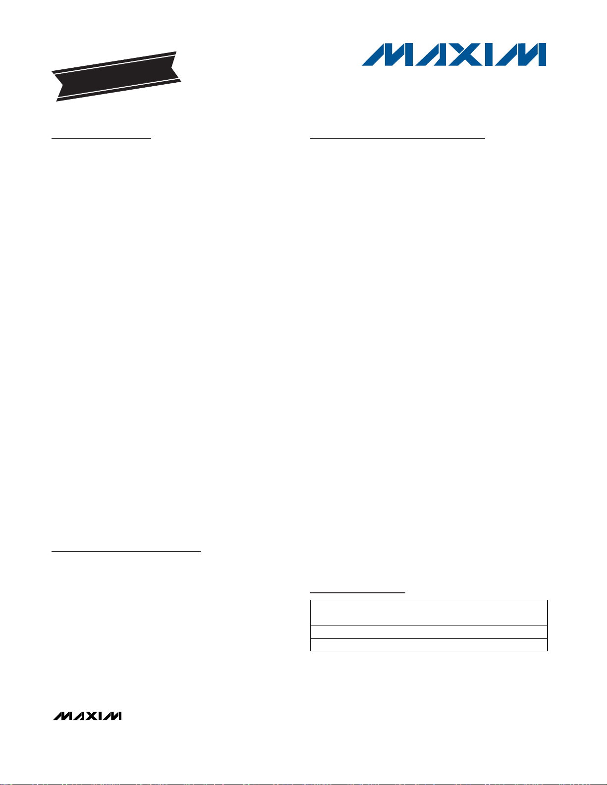
The MAX3421E connects to any microprocessor (µP)
using 3 or 4 interface pins (Figure 1). On a simple
microprocessor without SPI hardware, these can be
bit-banged general-purpose I/O pins. Eight GPIN and
eight GPOUT pins on the MAX3421E more than
replace the µP pins necessary to implement the interface. Although the MAX3421E SPI hardware includes
separate data-in (MOSI, master-out, slave-in) and dataout (MISO, master-in, slave-out) pins, the SPI interface
can also be configured for the MOSI pin to carry bidirectional data, saving an interface pin. This is referred
to as half-duplex mode.
Typical Application Circuits
3.3V
REGULATOR
SPI
3, 4
INT
USB
μ
P
MAX3421E
Figure 1. The MAX3421E Connects to Any Microprocessor
Using 3 or 4 Interface Pins
Page 3
MAX3421E
USB Peripheral/Host Controller
with SPI Interface
_______________________________________________________________________________________ 3
3.3V
REGULATOR
POWER RAIL
ASIC,
DSP,
ETC.
SPI
3, 4
INT
MAX3421E
USB
Figure 2. The MAX3421E Connected to a Large Chip
3.3V
REGULATOR
MISO
LOCAL
GND
LOCAL
POWER
INT
MAX3421E
SCLK
MOSI
SS
MICRO
ASIC
DSP
I
S
O
L
A
T
O
R
S
USB
Figure 3. Optical Isolation of USB Using the MAX3421E
MICRO,
ASIC,
DSP
USB
PERIPHERAL
USB
"A"
USB
"B"
V
BUS
SWITCH
FAULT
5V
SPI
3, 4
INT
V
BUS
D+
D-
GND
V
BUS
POWER
ON/OFF
3.3V
REGULATOR
MAX3421E
Figure 4. The MAX3421E in an Embedded Host Application
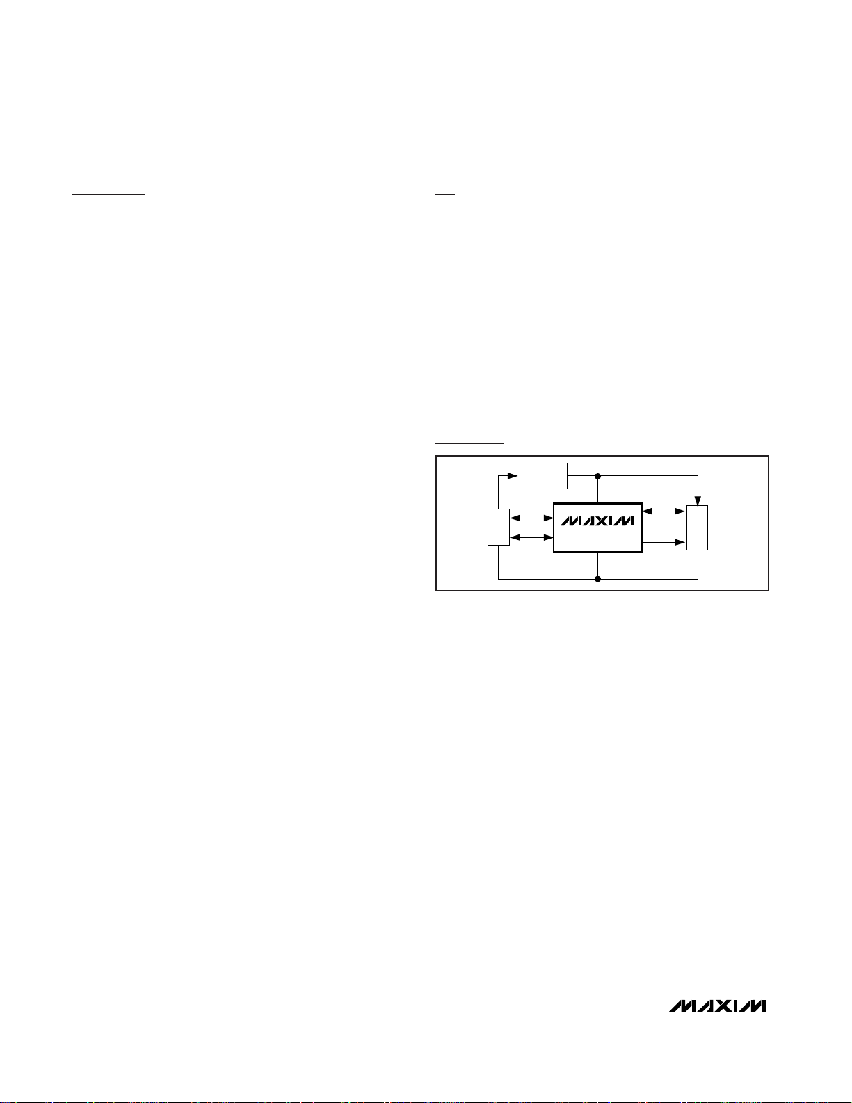
Two MAX3421E features make it easy to connect to
large, fast chips such as ASICs and DSPs (Figure 2).
First, the SPI interface can be clocked up to 26MHz.
Second, the VLpin and internal level translators allow
running the system interface at a lower voltage than
the 3.3V required for VCC.
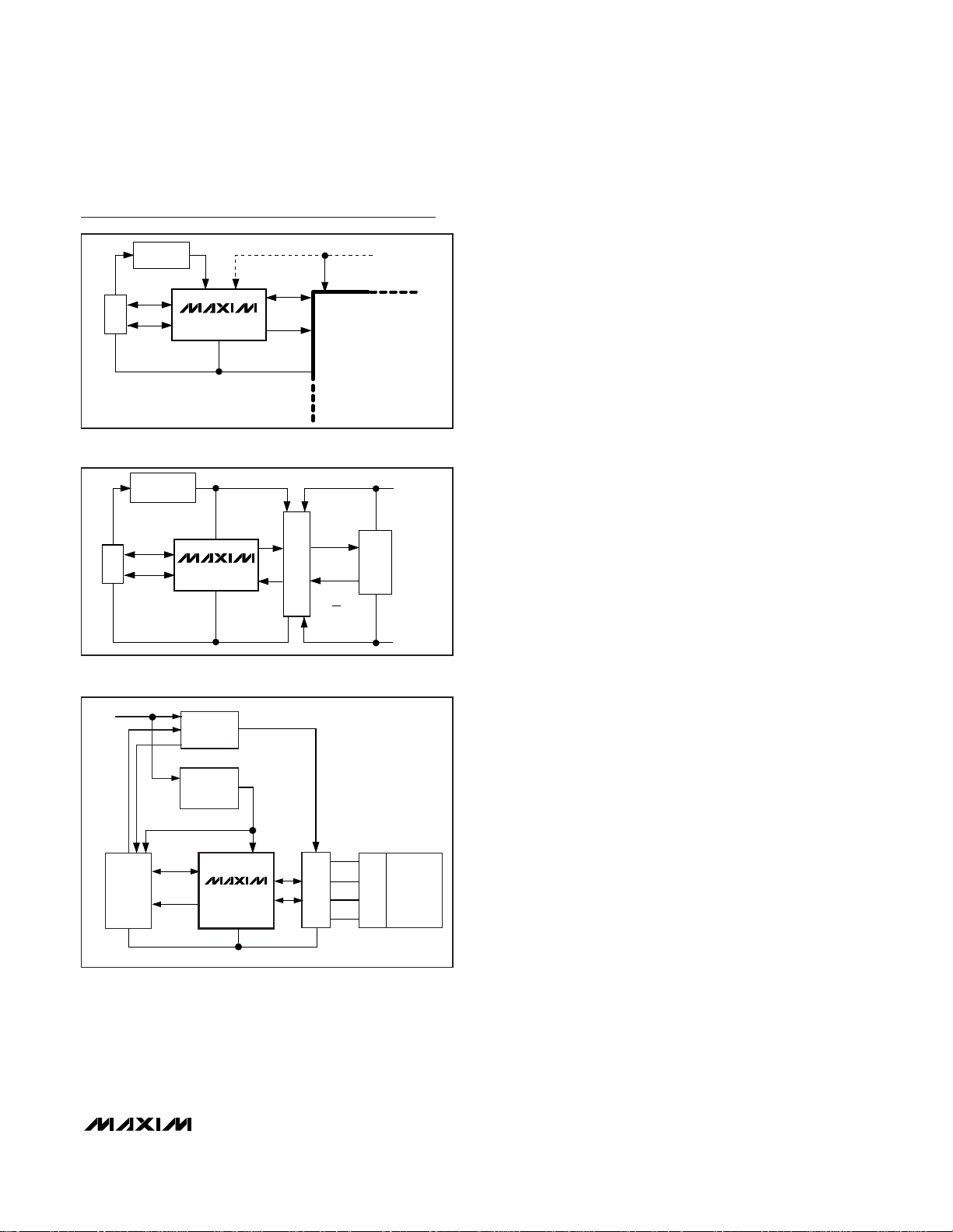
The MAX3421E provides an ideal method for electrically
isolating a USB interface (Figure 3). USB employs flow
control in which the MAX3421E automatically answers
host requests with a NAK handshake, until the microprocessor completes its data-transfer operations over
the SPI port. This means that the SPI interface can run
at any frequency up to 26MHz. Therefore, the designer
is free to choose the interface operating frequency and
to make opto-isolator choices optimized for cost or performance.
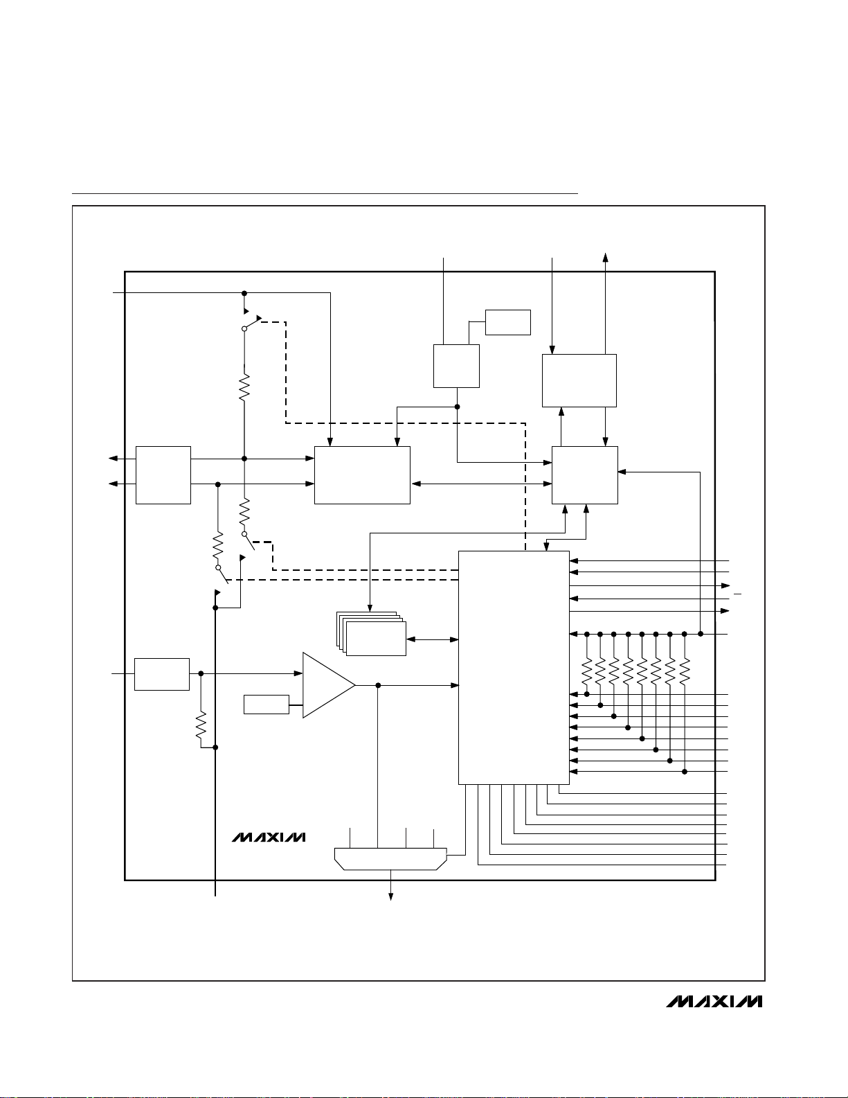
Figure 4 shows a block diagram for a system in which
the MAX3421E operates as a USB host. A USB host
supplies 5V power to the V
BUS
pin of the USB “A” connector to power USB peripherals. A system that provides power to an external peripheral should use
protection circuitry on the power pin to prevent an
external overcurrent situation from damaging the system. A V
BUS
switch, such as the MAX4789, provides
power control plus two additional features: it limits the
current delivered to the peripheral (for example to
200mA), and it indicates a fault (overcurrent) condition
to the SPI controller. Maxim offers a variety of V
BUS
switches with various current limits and features.
Consult the Maxim website for details.
A 3.3V regulator (for example, the MAX6349TL) powers
the MAX3421E, and optionally the system controller. If
the system controller operates with a lower voltage, the
MAX3421E SPI and I/O interface can run at the lower
voltage by connecting the system voltage (for example, 2.5V or 1.8V) to the MAX3421E VLpin.
Typical Application Circuits (continued)
Page 4
MAX3421E
USB Peripheral/Host Controller
with SPI Interface
4 _______________________________________________________________________________________
Functional Diagram
GPIN0
1V TO 3V
VBCOMP
D-
D+
V
CC
R
GPIN
V
BUS
COMP
SS
MISO
SCLK
INT
SPI SLAVE
INTERFACE
USB SIE
(SERIAL-
INTERFACE
ENGINE)
FULL-SPEED/
LOW-SPEED
USB
TRANSCEIVER
RESET
LOGIC
1.5kΩ
INTERNAL
POR
RES XI XO
POWER
DOWN
OSC
AND
4x PLL
48MHz
ESD
PROTECTION
ESD
PROTECTION
GPX
OPERATE
SOF
BUSACT/
INIRQ
MUX
0123
MOSI
VBUS_DET
ENDPOINT
BUFFERS
MAX3421E
GND
GPIN1
GPIN2
GPIN3
GPIN4
GPIN5
GPIN6
GPIN7
GPOUT0
GPOUT1
GPOUT2
GPOUT3
GPOUT4
GPOUT5
GPOUT6
GPOUT7
V
L
R
IN
15kΩ
15kΩ
Page 5
MAX3421E
USB Peripheral/Host Controller
with SPI Interface
_______________________________________________________________________________________ 5
Pin Description
PIN NAME
INPUT/
FUNCTION
1 GPIN7 Input
General-Purpose Input. GPIN7–GPIN0 are connected to V
L
with internal pullup resistors.
GPIN7–GPIN0 logic levels are referenced to the voltage on V
L
.
2VLInput
Level-Translator Voltage Input. Connect V
L
to the system’s 1.4V to 3.6V logic-level power
supply. Bypass V
L
to ground with a 0.1µF capacitor as close to VL as possible.
3, 19 GND Input Ground
4
5
6
7
8
9
10
11
General-Purpose Push-Pull Outputs. GPOUT7–GPOUT0 logic levels are referenced to the
voltage on V
L
.
12 RES Input
Device Reset. Drive RES low to clear all of the internal registers except for PINCTL (R17),
USBCTL (R15), and SPI logic. The logic level is referenced to the voltage on V
L
. (See the
Device Reset section for a description of resets available on the MAX3421E.) Note: The
MAX3421E is internally reset if either V
C C
or V L is not present. The register file is not accessible
under these conditions.
13 SCLK Input
S P I S er i al - C l ock Inp ut. An exter nal S P I m aster sup p l i es S C LK w i th fr eq uenci es up to 26M H z. The
l og i c l evel i s r efer enced to the vol tag e on V
L
. D ata i s cl ocked i nto the S P I sl ave i nter face on the
r i si ng ed g e of S C LK. D ata i s cl ocked out of the S P I sl ave i nter face on the fal l i ng ed g e of S C LK.
14 SS Input
SPI Slave Select Input. The SS logic level is referenced to the voltage on V
L
. When SS is driven
high, the SPI slave interface is not selected, the MISO pin is high impedance, and SCLK
transitions are ignored. An SPI transfer begins with a high-to-low SS transition and ends with a
low-to-high SS transition.
15 MISO
SPI Serial-Data Output (Master-In Slave-Out). MISO is a push-pull output. MISO is tri-stated in
half-duplex mode or when SS = 1. The MISO logic level is referenced to the voltage on V
L
.
16 MOSI
Input or
Input/
SPI Serial-Data Input (Master-Out Slave-In). The logic level on MOSI is referenced to the
voltage on V
L
. MOSI can also be configured as a bidirectional MOSI/MISO input and output.
(See Figure 15.)
17 GPX
G ener al - P ur p ose M ul ti p l exed P ush- P ul l O utp ut. The i nter nal M AX 3421E si g nal that ap p ear s on
G P X i s p r og r am m ab l e b y w r i ti ng to the G P X B and G P X A b i ts of the P IN C TL ( R17) r eg i ster and the
S E P IRQ b i t of the M O D E ( R27) r eg i ster . GP X i nd i cates one of fi ve si g nal s ( see the G P X secti
on) .
18 INT
Interrupt Output. In edge mode, the logic level on INT is referenced to the voltage on VL and is
a push-pull output with programmable polarity. In level mode, INT is open-drain and active low.
Set the IE bit in the CPUCTL (R16) register to enable INT.
20 D-
Input/
USB D- Signal. Connect D- to a USB connector through a 33Ω ±1% series resistor. A
switchable 15kΩ D- pulldown resistor is internal to the device.
OUTPUT
GPOUT0
GPOUT1
GPOUT2
GPOUT3
GPOUT4
GPOUT5
GPOUT6
GPOUT7
Output
Output
Output
Output
Output
Output
Page 6
MAX3421E
USB Peripheral/Host Controller
with SPI Interface
6 _______________________________________________________________________________________
Pin Description (continued)
PIN NAME
INPUT/
FUNCTION
21 D+
Input/
USB D+ Signal. Connect D+ to a USB connector through a 33Ω ±1% series resistor. A
switchable 1.5kΩ D+ pullup resistor and 15kΩ D+ pulldown resistor is internal to the device.
22
Input
V
BUS
Comparator Input. VBCOMP is internally connected to a voltage comparator to allow the
SPI master to detect (through an interrupt or checking a register bit) the presence or loss of
power on V
BUS
. Bypass VBCOMP to ground with a 1.0µF ceramic capacitor. VBCOMP is pulled
down to ground with R
IN
(see Electrical Characteristics).
23 V
CC
Input
U S B Tr anscei ver and Log i c C or e P ow er - S up p l y Inp ut. C onnect V
C C
to a p osi ti ve 3.3V p ow er
24 XI Input
Crystal Oscillator Input. Connect XI to one side of a parallel resonant 12MHz ±0.25% crystal
and a load capacitor to GND. XI can also be driven by an external clock referenced to V
CC
.
25 XO
C r ystal Osci l l ator O utp ut. C onnect X O to the other si d e of a p ar al l el r esonant 12M H z ± 0.25% cr ystal
and a l oad cap aci tor to GN D . Leave X O unconnected i f X I i s d r i ven w i th an exter nal sour ce.
26 GPIN0
27 GPIN1
28 GPIN2
29 GPIN3
30 GPIN4
31 GPIN5
32 GPIN6
Input
General-Purpose Inputs. GPIN7–GPIN0 are connected to V
L
with internal pullup resistors.
GPIN7–GPIN0 logic levels are referenced to the voltage on V
L
.
EP GND Input
E xp osed P ad d l e, C onnected to Gr ound . C onnect E P to GN D or l eave unconnected . E P i s l ocated
on the b ottom of the TQFN p ackag e. The TQ FP p ackag e d oes not have an exp osed p ad d l e.
OUTPUT
Output
VBCOMP
sup p l y. Byp ass V
Output
to g r ound w i th a 1.0µF cer am i c cap aci tor as cl ose to the V
C C
p i n as p ossi b l e.
C C
Page 7
MAX3421E
USB Peripheral/Host Controller
with SPI Interface
_______________________________________________________________________________________ 7
Register Description
The SPI master controls the MAX3421E by reading and
writing 26 registers in peripheral mode (see Table 1) or
reading and writing 23 registers in host mode (see Table
2). Setting the HOST bit in the MODE (R27) register configures the MAX3421E for host operation. When operating
as a USB peripheral, the MAX3421E is register-compatible with the MAX3420E with the additional features listed
in Note 1b below Table 1. For a complete description of
register contents, refer to the MAX3421E Programming
Guide on the Maxim website.
A register access consists of the SPI master first writing
an SPI command byte followed by reading or writing the
contents of the addressed register. All SPI transfers are
MSB first. The command byte contains the register
address, a direction bit (read = 0, write = 1), and the
ACKSTAT bit (Figure 5). The SPI master addresses the
MAX3421E registers by writing the binary value of the
register number in the Reg4 through Reg0 bits of the
command byte. For example, to access the IOPINS1
(R20) register, the Reg4 through Reg0 bits would be as
follows: Reg4 = 1, Reg3 = 0, Reg2 = 1, Reg1 = 0, Reg0
= 0. The DIR (direction) bit determines the direction for
the data transfer. DIR = 1 means the data byte(s) are
written to the register, and DIR = 0 means the data
byte(s) are read from the register. The ACKSTAT bit sets
the ACKSTAT bit in the EPSTALLS (R9) register (peripheral mode only). The SPI master sets this bit to indicate
that it has finished servicing a CONTROL transfer. Since
the bit is frequently used, having it in the SPI command
byte improves firmware efficiency. The ACKSTAT bit is
ignored in host mode. In SPI full-duplex mode, the
MAX3421E clocks out eight USB status bits as the com-
mand byte is clocked in (Figures 6, 7). In half-duplex
mode, these status bits are accessed as register bits.
The first five registers (R0–R4) address FIFOs in both
peripheral and host modes. Repeated accesses to these
registers freeze the internal register address so that multiple bytes may be written to or read from a FIFO in the
same SPI access cycle (while SS is low). Accesses to
registers R5–R19 increment the internal register address
for every byte transferred during the SPI access cycle.
Accessing R20 freezes access at that register, accessing R21–R31 increments the internal address, and
repeated accesses to R31 freeze at R31.
The register maps in Table 1 and Table 2 show which
register bits apply in peripheral and host modes.
Register bits that do not apply to a particular mode are
shown as zeros. These register bits read as zero values
and should not be written to with a logic 1.
Register Map in Peripheral Mode
The MAX3421E maintains register compatibility with the
MAX3420E when operating in USB peripheral mode
(MAX3421E HOST bit is set to 0 (default)). Firmware
written for the MAX3420E runs without modification on
the MAX3421E. To support new MAX3421E features,
the register set includes new bits, described in Note 1b
at the bottom of Table 1.
Register Map in Host Mode
As Table 2 shows, in host mode (HOST = 1), some
MAX3420E registers are renamed (for example R1
becomes RCVFIFO), some are not used (shown with
zeros), and some still apply to host mode. In addition, 11
registers (R21–R31) add the USB host capability.
Figure 7. USB Status Bits Clocked Out as First Byte of Every Transfer in Host Mode (Full-Duplex Mode Only)
STATUS BITS (HOST MODE)
b7 b6 b5 b4 b3 b2 b1 b0
HXFRDNIRQ
CONNIRQ
BUSEVENTIRQ
*The ACKSTAT bit is ignored in host mode.
Figure 5. SPI Command Byte
b7 b6 b5 b4 b3 b2 b1 b0
Reg4 Reg3 Reg2 Reg1 Reg0 0 DIR
ACKSTAT*
Figure 6. USB Status Bits Clocked Out as First Byte of Every Transfer in Peripheral Mode (Full-Duplex Mode Only)
STATUS BITS (PERIPHERAL MODE)
b7 b6 b5 b4 b3 b2 b1 b0
SUSPIRQ URESIRQ
IN0BAVIRQ
SUDAVIRQ IN3BAVIRQ IN2BAVIRQ OUT1DAVIRQ OUT0DAVIRQ
FRAMEIRQ
SUSDNIRQ SNDBAVIRQ RCVDAVIRQ RSMREQIRQ
Page 8

MAX3421E
USB Peripheral/Host Controller
with SPI Interface
8 _______________________________________________________________________________________
Table 1. MAX3421E Register Map in Peripheral Mode (HOST = 0) (Notes 1a, 1b)
R EG
NAME b 7 b 6 b 5 b 4 b 3 b 2 b 1 b 0
a c c
R0
EP0 F IF O b 7b 6b 5b 4b 3b 2b 1b 0
RS C
R1
b 7b 6b 5b 4b 3b 2b 1b 0
RS C
R2
b 7b 6b 5b 4b 3b 2b 1b 0
RS C
R3
b 7b 6b 5b 4b 3b 2b 1b 0
RS C
R4
SU D F IF O b 7b 6b 5b 4b 3b 2b 1b 0
RS C
R5
EP0 B C 0b 6b 5b 4b 3b 2b 1b 0
RS C
R6
0b 6b 5b 4b 3b 2b 1b 0
RS C
R7
EP2 IN B C 0b 6b 5b 4b 3b 2b 1b 0
RS C
R8
EP3 IN B C 0b 6b 5b 4b 3b 2b 1b 0
RS C
R9
0
RS C
R10
C L R T O G S
00
RS C
R11
EPI R Q 00
RC
R12
EPI EN 00
RS C
R13
U SB IR Q
RC
R14
U SB IEN
V BU S IE
RS C
R15
U SB C T L
S IG RWU 0 0
RS C
R16
C PU C T L
000 0 0IE
RS C
R17
PIN C T L
P OS IN TGP X BGP X A
RS C
R18
R EVISIO N 00 010 0 1 0
R
R19
F N A D D R 0b 6b 5b 4b 3b 2b 1b 0
R
R20
IO PIN S1 GP IN 3GP IN 2GP IN 1GP IN 0
GP O U T2 GP O U T1
RS C
R21
IOPINS2
GP IN 7GP IN 6GP IN 5GP IN 4
GP O U T6 GP O U T5
RS C
R22
GPINIRQ
RS C
R23
GPINIEN
RS C
R24
GPINPOL
RS C
R25
—
00 000 0 0 0
—
R26
—
00 000 0 0 0
—
R27
MODE
00 0
00 0
RS C
R28
—
00 000 0 0 0
—
R29
—
00 000 0 0 0
—
R30
—
00 000 0 0 0
—
R31
—
00 000 0 0 0
—
Note 1a: The acc (access) column indicates how the SPI master can access the register.
R = read, RC = read or clear, RSC = read, set, or clear.
Writing to an R register (read only) has no effect.
Writing a 1 to an RC bit (read or clear) clears the bit.
Writing a zero to an RC bit has no effect.
EP1 O U T F IF O
EP2 IN F IF O
EP3 IN F IF O
EP1 O U T B C
EPST A L L S
E P 3D IS AB E P 2D IS AB E P 1D IS AB C TG E P 3IN C TG E P 2IN C TG E P 1OU T
U RE S D N IRQ V BU S IRQ N OV BU S IRQ S U S P IRQ U RE S IRQ BU S AC TIRQ RWU D N IRQ OS C OKIRQ
U RE S D N IE
H OS C S TE N V BG ATE C H IP RE S P WRD OWN C ON N E C T
P U LS E WID 1P U LS E WID 0
E P 3IN AK E P 2IN AK E P 0IN AK FD U P S P IIN TLE V E L
GP IN IRQ7 GP IN IRQ6 GP IN IRQ5 GP IN IRQ4 GP IN IRQ3 GP IN IRQ2 GP IN IRQ1 GP IN IRQ0
GP IN IE N 7GP IN IE N 6GP IN IE N 5GP IN IE N 4GP IN IE N 3GP IN IE N 2GP IN IE N 1GP IN IE N 0
GP IN P OL7 GP IN P OL6 GP IN P OL5 GP IN P OL4 GP IN P OL3 GP IN P OL2 GP IN P OL1 GP IN P OL0
AC KS TAT S TLS TAT S TLE P 3IN S TLE P 2IN S TLE P 1OU TS TLE P 0OU TS TLE P 0IN
S U D AV IRQ IN 3BAV IRQ IN 2BAV IRQ OU T1D AV IRQ OU T0D AV IRQ IN 0BAV IRQ
S U D AV IE IN 3BAV IE IN 2BAV IE OU T1D AV IE OU T0D AV IE IN 0BAV IE
N OV BU S IE S U S P IE U RE S IE BU S AC TIE RWU D N IE OS C OKIE
GP O U T3
GP O U T7
S E P IRQ
GP O U T0
GP O U T4
H OS T = 0
Page 9

MAX3421E
USB Peripheral/Host Controller
with SPI Interface
_______________________________________________________________________________________ 9
Note 1b: In peripheral mode, the MAX3421E performs identically to the MAX3420E with the following enhancements:
1) R16 adds the PULSEWID0 and PULSEWID1 bits to control the INT pulse width in edge interrupt mode
(see Figure 12.) These bits default to the MAX3420E setting of 10.6µs.
2) R21 adds four more GPIO bits.
3) R22 and R23 add general-purpose input pins to the interrupt system. R24 controls the edge polarity.
4) R27 controls the peripheral/host mode and the SEPIRQ bit.
5) When [GPXB:GPXA] = [1:0] and the bit SEPIRQ = 1 (R27 bit 4), the GPX output replaces the BUSACT
signal with a second IRQ pin dedicated to the GPIN pin interrupts.
Table 2. MAX3421E Register Map in Host Mode (HOST = 1) (Note 2)
R EG
b 7 b 6 b 5 b 4 b 3 b 2 b 1 b 0
a c c
R0
—00000000—
R1
b 7b 6b 5b 4b 3b 2b 1b 0
RS C
R2
b 7b 6b 5b 4b 3b 2b 1b 0
RS C
R3
—00000000—
R4
b 7b 6b 5b 4b 3b 2b 1b 0
RS C
R5
—00000000—
R6
RCVBC
0BC 6BC 5BC 4BC 3BC 2BC 1BC 0
RS C
R7
SNDBC
0BC 6BC 5BC 4BC 3BC 2BC 1BC 0
RS C
R8
—
00000 0 0 0—
R9
—
00000 0 0 0—
R10
—
00000 0 0 0—
R11
—
00000 0 0 0—
R12
—
00000 0 0 0—
R13
USBIRQ
0
00 0 0
RC
R14
USBIEN
0V BU S IE
00 0 0OS C OKIE
RS C
R15
USBCTL
00
00 0 0
RS C
R16
CPUCTL
00 0 0 0 IE
RS C
R17
PINCTL
E P 3IN AK
P OS IN TGP X BGP X A
RS C
R18
00010 0 1 0R
R19
—
00000 0 0 0—
R20
IOPINS1
GP IN 3GP IN 2GP IN 1GP IN 0GP O U T3 GP O U T2 GP O U T1 GP O U T0
RS C
R21
IOPINS2
GP IN 7GP IN 6GP IN 5GP IN 4GP O U T7 GP O U T6 GP O U T5 GP O U T4
RS C
R22
GP IN IRQ0
RC
R23
GPINIEN
GP IN IE N 1GP IN IE N 0
RS C
R24
GP IN P OL0
RS C
R25
HIRQ
RC
R26
HIEN
RS C
R27
MODE
H U BP RE S P E E D H OS T = 1
RS C
R28
0b 6b 5b 4b 3b 2b 1b 0
RS C
R29
HCTL
S IG RS M
FRM RS TBU S RS TLS
R30
HXFR
H S IS O
S E TU P E P 3E P 2E P 1E P 0LS
R31
HRSL
H RS LT3 H RS LT2 H RS LT1 H RS LT0 R
Table 1. MAX3421E Register Map in Peripheral Mode (HOST = 0) (Notes 1a, 1b) (continued)
NAME
RCVFIFO
SNDFIFO
SUDFIFO
REVISION
GPINIRQ
GPINPOL
PERADDR
P U LS E WID 1P U LS E WID 0
GP IN IRQ7 GP IN IRQ6 GP IN IRQ5 GP IN IRQ4 GP IN IRQ3 GP IN IRQ2 GP IN IRQ1
GP IN IE N 7GP IN IE N 6GP IN IE N 5GP IN IE N 4GP IN IE N 3GP IN IE N 2
GP IN P OL7 GP IN P OL6 GP IN P OL5 GP IN P OL4 GP IN P OL3 GP IN P OL2 GP IN P OL1
H X FRD N IRQ FRAM E IRQ C ON N IRQ S U S D N IRQ S N D BAV IRQ RC V D AV IRQ RS M RE QIRQ BU S E V E N TIRQ
H X FRD N IE FRAM E IE C ON N IE S U S D N IE S N D BAV IE RC V D AV IE RS M RE QIE BU S E V E N TIE
D P P U LLD N D M P U LLD N D E LAY IS OS E P IRQ S OFKAE N AB
S N D TOG1 S N D TOG0 RC V TOG1 RC V TOG0
JS TATU S KS TATU S S N D TOGRD RC V TOGRD
V BU S IRQ N OV BU S IRQ
N OV BU S IE
C H IP RE S P WRD OWN
E P 2IN AK E P 0IN AK FD U P S P IIN TLE V E L
BU S S AM P LE
OU TN IN
OS C OKIRQ
Page 10
MAX3421E
USB Peripheral/Host Controller
with SPI Interface
10 ______________________________________________________________________________________
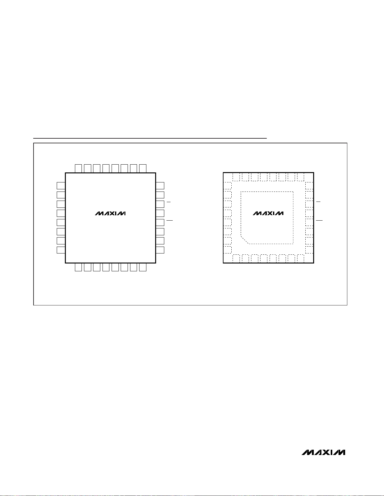
MAX3421E
TQFP
(5mm x 5mm)
TOP VIEW
29
30
28
27
12
11
13
V
L
GPOUT0
GPOUT1
GPOUT2
GPOUT3
14
GPIN7
V
CC
D+
D-XIGND
INT
12
GPIN2
4567
2324 22 20 19 18
GPIN3
GPIN4
SS
SCLK
RES
GPOUT7
GND
VBCOMP
3
21
31
10
GPIN5
GPOUT6
32
9
GPIN6
GPOUT5
GPIN1
26
15
MISO
GPIN0
25
16
MOSI
GPOUT4
GPX
8
17
XO
+
Pin Configurations
Note 2: The acc (access) column indicates how the SPI master can access the register.
R = read; RC = read or clear; RSC = read, set, or clear; LS = load-sensitive.
Writing to an R register (read only) has no effect.
Writing a 1 to an RC bit (read or clear) clears the bit.
Writing a zero to an RC bit has no effect.
Writing to an LS register initiates a host operation based on the contents of the register.
MAX3421E
TQFN
(5mm x 5mm)
TOP VIEW OF BOTTOM LEADS
29
30
28
27
12
11
13
V
L
GPOUT0
GPOUT1
GPOUT2
GPOUT3
14
GPIN7
V
CC
D+
D-XIGND
INT
12
GPIN2
4567
2324 22 20 19 18
GPIN3
GPIN4
SS
SCLK
RES
GPOUT7
GND
VBCOMP
3
21
31
10
GPIN5
GPOUT6
32
9
GPIN6
GPOUT5
GPIN1
26
15
MISO
GPIN0
25
16
MOSI
GPOUT4
GPX
8
17
XO
+
*EXPOSED PADDLE CONNECTED TO GROUND
*EP
Table 2. MAX3421E Register Map in Host Mode (HOST = 1) (Note 2) (continued)
Page 11

MAX3421E
USB Peripheral/Host Controller
with SPI Interface
______________________________________________________________________________________ 11
ABSOLUTE MAXIMUM RATINGS
ELECTRICAL CHARACTERISTICS
(VCC= +3V to +3.6V, VL= +1.4V to +3.6V, TA= T
MIN
to T
MAX
, unless otherwise noted. Typical values are at VCC= +3.3V, VL=
+2.5V, T
A
= +25°C.) (Note 3)
Stresses beyond those listed under “Absolute Maximum Ratings” may cause permanent damage to the device. These are stress ratings only, and functional
operation of the device at these or any other conditions beyond those indicated in the operational sections of the specifications is not implied. Exposure to
absolute maximum rating conditions for extended periods may affect device reliability.
(All voltages referenced to GND, unless otherwise noted.)
V
CC
......................................................................... -0.3V to +4V
V
L
.............................................................................-0.3V to +4V
VBCOMP .................................................................-0.3V to +6V
D+, D-, XI, XO ............................................-0.3V to (V
CC
+ 0.3V)
SCLK, MOSI, MISO, SS, RES, GPOUT7–GPOUT0,
GPIN7–GPIN0, GPX, INT ..........................-0.3V to (V
L
+ 0.3V)
Continuous Power Dissipation (T
A
= +70°C)
32-Pin TQFN (derate 21.3mW/°C above +70°C) .......1702mW
32-Pin TQFP (derate 13.1mW/°C above +70°C)........1047mW
Operating Temperature Range ...........................-40°C to +85°C
Junction Temperature......................................................+150°C
Storage Temperature Range .............................-65°C to +150°C
Lead Temperature (soldering, 10s) .................................+300°C
PARAMETER
CONDITIONS
UNITS
DC CHARACTERISTICS
Supply Voltage V
CC
V
CC
3.0 3.3 3.6 V
Logic-Interface Voltage V
L
V
L
1.4 3.6 V
VCC Supply Current I
CC
Continuously transmitting on D+ and D- at
12Mbps, C
L
= 50pF on D+ and D- to GND,
CONNECT = 0
45 mA
VL Supply Current I
L
SCLK toggling at 20MHz, SS = low,
GPIN7–GPIN0 = 0
10 mA
V
CC
Supply Current During Idle I
CCID
D+ = high, D- = low 8.7 15 mA
VCC Suspend Supply Current I
CCSUS
CONNECT = 0, PWRDOWN = 1 30 60 µA
V L S usp end S up p l y C urr ent I
LSUS
CONNECT = 0, PWRDOWN = 1 20 50 µA
LOGIC-SIDE I/O
I
LOAD
= +1mA
I
LOAD
= +5mA, VL < 2.5V (Note 4)
MISO, GPOUT7–GPOUT0, GPX,
INT Output High Voltage
V
OH
I
LOAD
= +10mA, VL ≥ 2.5V (Note 4)
V
I
LOAD
= -1mA 0.4
I
LOAD
= -20mA, VL < 2.5V (Note 4) 0.6
MISO, GPOUT7–GPOUT0, GPX,
INT Output Low Voltage
V
OL
I
LOAD
= -20mA, VL ≥ 2.5V (Note 4) 0.4
V
SCLK, MOSI, GPIN7–GPIN0, SS,
RES Input High Voltage
V
IH
V
SCLK, MOSI, GPIN7–GPIN0, SS,
RES Input Low Voltage
V
IL
0.4 V
SCLK, MOSI, SS, RES Input
Leakage Current
I
IL
-1 +1 µA
GP IN 7–GP IN 0 P ul l up Resi stor to V
L
R
GPIN
10 20 30 kΩ
TRANSCEIVER SPECIFICATIONS
Differential-Receiver Input
Sensitivity
|V
D+
- VD-| 0.2 V
SYMBOL
MIN TYP MAX
2.35
V L - 0.4
V L - 0.45
V L - 0.4
2/3 x V
L
Page 12

MAX3421E
USB Peripheral/Host Controller
with SPI Interface
12 ______________________________________________________________________________________
ELECTRICAL CHARACTERISTICS (continued)
(VCC= +3V to +3.6V, VL= +1.4V to +3.6V, TA= T
MIN
to T
MAX
, unless otherwise noted. Typical values are at VCC= +3.3V, VL=
+2.5V, T
A
= +25°C.) (Note 3)
PARAMETER
CONDITIONS
Differential-Receiver CommonMode Voltage
0.8 2.5 V
Single-Ended Receiver Input Low
Voltage
V
IL
0.8 V
Single-Ended Receiver Input
High Voltage
V
IH
2.0 V
Single-Ended Receiver
Hysteresis Voltage
0.2 V
D+, D- Output Low Voltage V
OL
RL = 1.5kΩ from D+ to 3.6V 0.3 V
D+, D- Output High Voltage V
OH
RL = 15kΩ from D+ and D- to GND 2.8 3.6 V
Driver Output Impedance
Excluding External Resistor
(Note 4) 2 7 11 Ω
D+ Pullup Resistor R
EXT
= 33Ω
1.5
kΩ
D+, D- Pulldown Resistor R
EXT
= 33Ω
15
kΩ
D+, D- Input Impedance 300 kΩ
ESD PROTECTION (D+, D-, VBCOMP)
Human Body Model
1µF ceramic capacitors from VBCOMP and
V
CC
to GND
kV
IEC 61000-4-2 Air-Gap Discharge
1µF ceramic capacitors from VBCOMP and
V
CC
to GND
kV
IEC 61000-4-2 Contact Discharge
1µF ceramic capacitors from VBCOMP and
V
CC
to GND
±8 kV
THERMAL SHUTDOWN
Thermal-Shutdown Low-to-High
°C
Thermal-Shutdown High-to-Low
°C
CRYSTAL OSCILLATOR SPECIFICATIONS (XI, XO)
XI Input High Voltage
V
XI Input Low Voltage 0.4 V
XI Input Current 10 µA
XI, XO Input Capacitance 3pF
VBCOMP COMPARATOR SPECIFICATIONS
VBCOMP Comparator Threshold
V
TH
1.0 2.0 3.0 V
VBCOMP Comparator Hysteresis
V
HYS
mV
VBCOMP Comparator Input
Impedance
R
IN
100 kΩ
SYMBOL
MIN TYP MAX UNITS
1.425
14.25
C C
±15
±12
+160
+140
375
2/3 x V
1.575
15.75
V
CC
Page 13

MAX3421E
USB Peripheral/Host Controller
with SPI Interface
______________________________________________________________________________________ 13
Note 3: Parameters are 100% production tested at TA= +25°C. Specifications over temperature are guaranteed by design.
Note 4: Guaranteed by bench testing. Limits are not production tested.
Note 5: At V
L
= 1.4V to 2.5V, derate all the SPI timing characteristics by 50%. Not production tested.
Note 6: The minimum period is derived from SPI timing parameters.
Note 7: Time-to-exit suspend is dependent on the crystal used.
PARAMETER
CONDITIONS
UNITS
USB TRANSMITTER TIMING CHARACTERISTICS (FULL-SPEED MODE)
D+, D- Rise Time t
RISE
CL = 50pF, Figures 8 and 9 4 20 ns
D+, D- Fall Time t
FALL
CL = 50pF, Figures 8 and 9 4 20 ns
Rise-/Fall-Time Matching CL = 50pF, Figures 8 and 9 (Note 4) 90 110 %
Output-Signal Crossover Voltage
CL = 50pF, Figures 8 and 9 (Note 4) 1.3 2.0 V
USB TRANSMITTER TIMING CHARACTERISTICS (HOST LOW-SPEED MODE)
D+, D- Rise Time t
RISE
200pF ≤ CL ≤ 600pF, Figures 8 and 9 75 300 ns
D+, D- Fall Time t
FALL
200pF ≤ CL ≤ 600pF, Figures 8 and 9 75 300 ns
Rise-/Fall-Time Matching 200p F ≤ C L ≤ 600p F, Fi g ur es 8 and 9 80 120 %
Output-Signal Crossover Voltage
200p F ≤ C L ≤ 600p F, Fi g ur es 8 and 9 1.3 2.0 V
SPI BUS TIMING CHARACTERISTICS (VL = 2.5V) (Figures 10 and 11) (Note 5)
VL > 2.5V
S eri al C l ock ( SC LK) P eri od ( N ote 6) t
CP
VL = 1.4V
ns
SCLK Pulse-Width High t
CH
17 ns
SCLK Pulse-Width Low t
CL
17 ns
SS Fall to MISO Valid t
CSS
20 ns
SS Leading Time Before the First
SCLK Edge
t
L
30 ns
SS Trailing Time After the Last
SCLK Edge
t
T
30 ns
Data-In Setup Time t
DS
5ns
Data-In Hold Time t
DH
10 ns
SS Pulse High t
CSW
200 ns
SCLK Fall to MISO Propagation
Delay
t
DO
ns
SCLK Fall to MOSI Propagation
Delay
t
DI
ns
SCLK Fall to MOSI Drive t
ON
3.5 ns
SS High to MOSI High
Impedance
t
OFF
20 ns
SUSPEND TIMING CHARACTERISTICS
Time-to-Enter Suspend PWRDOWN = 1 to oscillator stop 5 µs
Time-to-Exit Suspend
3ms
TIMING CHARACTERISTICS
(V
CC
= +3V to +3.6V, VL= +1.4V to +3.6V, TA= T
MIN
to T
MAX
, unless otherwise noted. Typical values are at VCC= +3.3V, VL=
+2.5V, T
A
= +25°C.) (Note 3)
SYMBOL
PWRDOWN = 1 to 0 to OSCOKIRQ (Note 7)
MIN TYP MAX
38.4
77.7
14.2
14.2
Page 14

MAX3421E
USB Peripheral/Host Controller
with SPI Interface
14 ______________________________________________________________________________________
Test Circuits and Timing Diagrams
Figure 8. Rise and Fall Times
V
OL
V
OH
t
RISE
t
FALL
90%
10%
Figure 9. Load for D+/D- AC Measurements
MAX3421E
D+ OR D-
TEST
POINT
33Ω
15kΩ
C
L
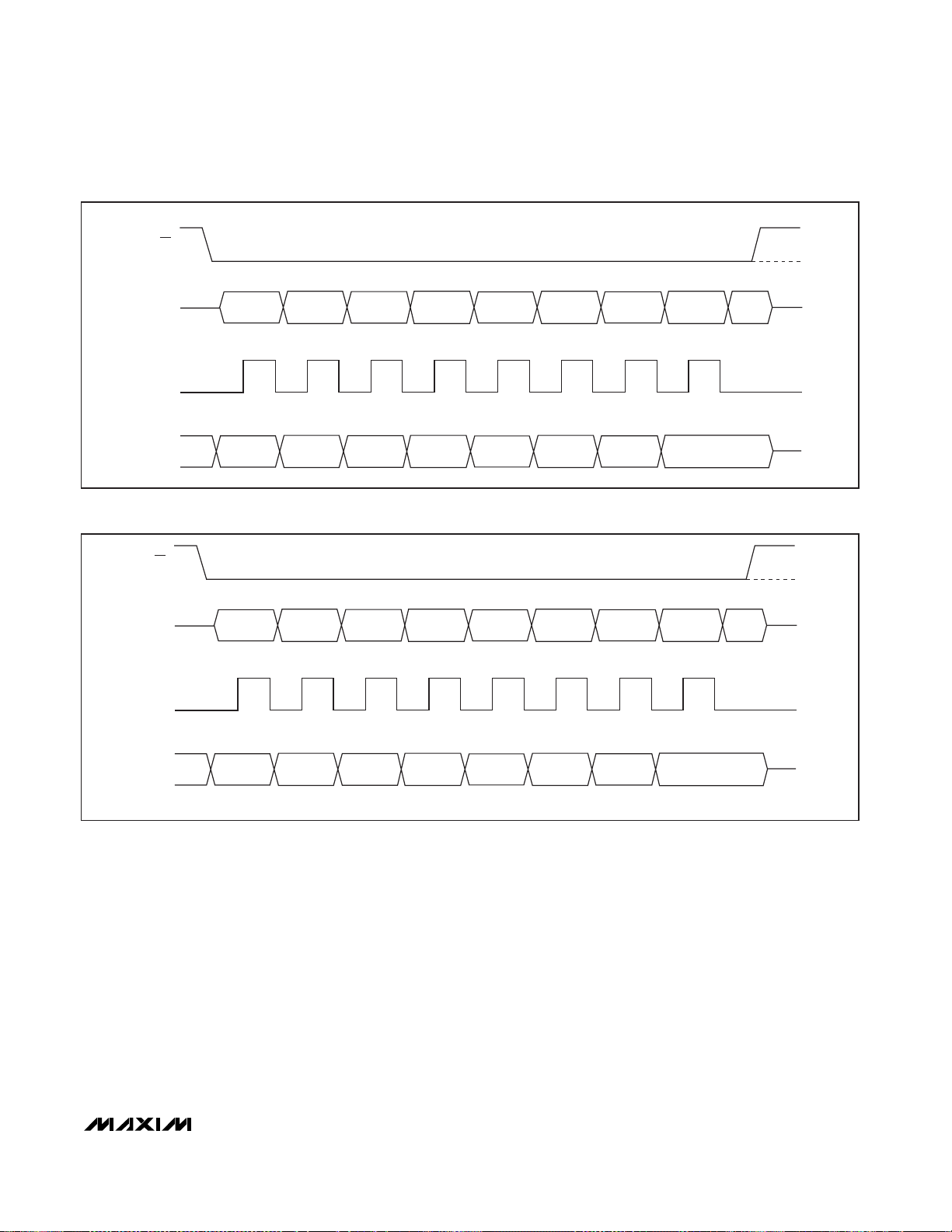
Figure 11. SPI Bus Timing Diagram (Half-Duplex Mode, SPI Mode (0,0))
SCLK
MOSI
MISO
NOTES:
1) DURING THE FIRST 8 CLOCKS CYCLES, THE MOSI PIN IS HIGH IMPEDANCE AND THE SPI MASTER DRIVES DATA ONTO THE MOSI PIN. SETUP AND HOLD TIMES ARE THE SAME AS
FOR FULL-DUPLEX MODE.
2) FOR SPI WRITE CYCLES, THE MOSI PIN CONTINUES TO BE HIGH IMPEDANCE AND THE EXTERNAL MASTER CONTINUES TO DRIVE MOSI.
3) FOR SPI READ CYCLES, AFTER THE 8TH CLOCK-FALLING EDGE, THE MAX3421E STARTS DRIVING THE MOSI PIN AFTER TIME t
ON
. THE EXTERNAL MASTER MUST TURN
OFF ITS DRIVER TO THE MOSI PIN BEFORE t
ON
TO AVOID CONTENTION. PROPAGATION DELAYS ARE THE SAME AS FOR THE MOSI PIN IN FULL-DUPLEX MODE.
t
DS
t
DH
t
CLtCH
t
DI
t
OFF
t
T
SS
HI-Z
8
1
2
9
10 16
t
L
t
CSW
t
ON
t
CP
HIGH
IMPEDANCE
HIGH
IMPEDANCE
Figure 10. SPI Bus Timing Diagram (Full-Duplex Mode, SPI Mode (0,0))
SS
SCLK
MOSI
MISO
HIGH
IMPEDANCE
t
L
t
CSS
1
2
t
DS
t
DH
t
t
CH
CL
t
CP
DO
10 16
8
9
t
t
CSW
t
T
HIGH
IMPEDANCE
Page 15

MAX3421E
USB Peripheral/Host Controller
with SPI Interface
______________________________________________________________________________________ 15
Typical Operating Characteristics
(VCC= +3.3V, VL= +3.3V, TA= +25°C.)
Detailed Description
The MAX3421E contains digital logic and analog circuitry necessary to implement a full-speed USB peripheral or a full-/low-speed host compliant to USB
specification rev 2.0. The MAX3421E is selected to
operate as either a host or peripheral by writing to the
HOST bit in the MODE (R27) register. The MAX3421E
features an internal USB transceiver with ±15kV ESD
protection on D+, D-, and VBCOMP. A switchable
1.5kΩ pullup resistor is provided on D+ and switchable
15kΩ pulldown resistors are provided on both D+ and
D-. Any SPI master can communicate with the
MAX3421E through the SPI slave interface that operates in SPI mode (0,0) or (1,1). An SPI master accesses
the MAX3421E by reading and writing to internal registers. A typical data transfer consists of writing a first
byte that sets a register address and direction with
additional bytes reading or writing data to the register
or internal FIFO.
In peripheral mode, the MAX3421E contains 384 bytes
of endpoint buffer memory, implementing the following
endpoints:
• EP0: 64-byte bidirectional CONTROL endpoint
• EP1: 2 x 64-byte double-buffered BULK/INT
OUT endpoint
• EP2: 2 x 64-byte double-buffered BULK/INT IN
endpoint
• EP3: 64-byte BULK/INT IN endpoint
The choice to use EP1, EP2, EP3 as BULK or INTERRUPT endpoints is strictly a function of the endpoint
descriptors that the SPI master returns to the USB host
during enumeration.
In host mode, the MAX3421E contains 256 bytes of
send and receive FIFO memory:
• SNDFIFO: Send FIFO—double-buffered 64-byte
FIFO
• RCVFIFO: Receive FIFO—double-buffered 64-byte
FIFO
The host FIFOs can send SETUP, BULK, INTERRUPT,
and ISOCHRONOUS requests to a peripheral device, at
full speed or low speed. The MAX3421E accommodates
low-speed devices whether they are directly connected,
or connected through a USB hub. Because the
MAX3421E does much of the host housekeeping, it is
easy to program. The SPI master does a typical host
operation by setting the device address and endpoint,
launching a packet, and waiting for a completion interrupt. Then it examines transfer result bits to determine
how the peripheral responded. It automatically generates frame markers (full-speed SOF packets or lowspeed keep-alive pulses), and ensures that packets are
dispatched at the correct times relative to these markers.
The MAX3421E register set and SPI interface is optimized
to reduce SPI traffic. An interrupt output pin, INT, notifies
the SPI master when USB service is required; for example, when a packet arrives, a packet is sent, or the host
suspends or resumes bus activity. Double-buffered FIFOs
EYE DIAGRAM
MAX3421E toc01
4
1
0
-1
01020304050607080
2
3
TIME (ns)
D+ AND D- (V)
Page 16

MAX3421E
USB Peripheral/Host Controller
with SPI Interface
16 ______________________________________________________________________________________
help sustain bandwidth by allowing data to move concurrently over USB and the SPI interface.
V
CC
Power the USB transceiver and digital logic by applying a positive 3.3V supply to VCC. Bypass VCCto GND
with a 1.0µF ceramic capacitor as close to the VCCpin
as possible.
V
L
VL acts as a reference level for the SPI interface and all
other digital inputs and outputs. Connect VLto the system’s logic-level power supply. Internal level translators
and VLallow the SPI interface and all general-purpose
inputs and outputs to operate at a system voltage
between 1.4V and 3.6V.
VBCOMP
The MAX3421E features a USB V
BUS
detector input,
VBCOMP. The VBCOMP pin can withstand input voltages up to 6V. Bypass VBCOMP to GND with a 1.0µF
ceramic capacitor. VBCOMP is internally connected to
a voltage comparator to allow the SPI master to detect
(through an interrupt or checking a register bit) the
presence or loss of power on V
BUS
. VBCOMP does not
power any internal circuitry inside the MAX3421E.
VBCOMP is pulled down to ground with RIN(see
Electrical Characteristics).
VBCOMP in Peripheral Mode
VBCOMP is internally connected to a voltage comparator so that the SPI master can detect the presence or
absence of V
BUS
. According to the USB 2.0 specifica-
tion, a self-powered peripheral must disconnect its
1.5kΩ pullup resistor to D+ in the event that the host
turns off bus power. The VBGATE bit in the USBCTL
(R15) register provides the option for the MAX3421E
internal logic to automatically disconnect the 1.5kΩ
resistor on D+. The VBGATE and CONNECT bits of
USBCTL (R15), along with the VBCOMP comparator
output (VBUS_DET), control the pullup resistor between
VCCand D+ as shown in Table 3 and the Functional
Diagram. Note that if VBGATE = 1 and VBUS_DET = 0,
the pullup resistor is disconnected regardless of the
CONNECT bit setting. If the device using the
MAX3421E is bus powered (through a +3.3V regulator
connected to VCC), the MAX3421E VBCOMP input can
be used as a general-purpose input. See the
Applications Information section for more details about
this connection.
VBCOMP in Host Mode
When using the MAX3421E in host mode, the presence
of V
BUS
does not need to be detected. In this case, the
VBCOMP input can be used as a general-purpose
input.
D+ and D-
The internal USB full-/low-speed transceiver is brought
out to the bidirectional data pins D+ and D-. These pins
are ±15kV ESD protected. Connect D+ and D- to a
USB B connector through 33Ω ±1% series resistors.
D+ and D- in Peripheral Mode
In peripheral mode, the D+ and D- pins connect to a
USB B connector through series resistors. A switchable
1.5kΩ pullup resistor is internally connected to D+.
D+ and D- in Host Mode
In host mode, the D+ and D- pins connect to a USB A
connector through series resistors. Switchable 15kΩ
pulldown resistors are internally connected to D+ and
D-. The DPPULLDN and DMPULLDN bits in the MODE
(R27) register control the connection between D+ and
D- to GND. For host operation, set these bits to 1 to
enable the pulldown resistors. A host interrupt bit called
CONNIRQ alerts the SPI master when a peripheral is
attached or detached.
XI and XO
XI and XO connect an external 12MHz crystal to the
internal oscillator circuit. XI is the crystal oscillator
input, and XO is the crystal oscillator output. Connect
one side of a 12MHz ±0.25% parallel resonant crystal
to XI, and connect XO to the other side. Connect load
capacitors (20pF max) to ground on both XI and XO. XI
can also be driven with an external 12MHz ±0.25%
clock. If driving XI with an external clock, leave XO
unconnected. The external clock must meet the voltage
characteristics depicted in the Electrical Character-
istics table. Internal logic is single-edge triggered. The
external clock should have a nominal 50% duty cycle.
Table 3. Internal Pullup Resistor Control
in Peripheral Mode
CONNECT
PULLUP
0 X X Not Connected
1 0 X Connected
1 1 0 Not Connected
1 1 1 Connected
VBGATE VBUS_DET
Page 17

MAX3421E
USB Peripheral/Host Controller
with SPI Interface
______________________________________________________________________________________ 17
RES
Drive RES low to put the MAX3421E into a chip reset. A
chip reset sets all registers to their default states,
except for PINCTL (R17), USBCTL (R15), and SPI logic.
All FIFO contents are unknown during chip reset. Bring
the MAX3421E out of chip reset by driving RES high.
The RES pulse width can be as short as 200ns. See the
Device Reset section for a description of the resets
available on the MAX3421E.
INT
The MAX3421E INT output pin signals when a USB
event occurs that requires the attention of the SPI master. INT can also be configured to assert when any of
the general-purpose inputs (GPIN0–GPIN7) are activated (see the GPIN7–GPIN0 section for more details).
The SPI master must set the IE bit in the CPUCTL (R16)
register to activate INT. When the IE bit is cleared, INT
is inactive (open for level mode, high for negative edge,
low for positive edge). INT is inactive upon power-up or
after a chip reset (IE = 0).
The INT pin can be a push-pull or open-drain output.
Set the INTLEVEL bit of the PINCTL (R17) register high
to program the INT output pin to be an active-low level
open-drain output. An external pullup resistor to VLis
required for this setting. In level mode, the MAX3421E
drives INT low when any of the interrupt flags are set. If
multiple interrupts are pending, INT goes inactive only
when the SPI master clears the last active interrupt
request bit (Figure 12). The POSINT bit of the PINCTL
(R17) register has no effect on INT in level mode.
Clear the INTLEVEL bit to program INT to be an edge
active push-pull output. The active edge is programmable using the POSINT bit of the PINCTL (R17) register.
In edge mode, the MAX3421E produces an edge refer-
enced to VLany time an interrupt request is activated,
or when an interrupt request is cleared and others are
pending (Figure 12). Set the POSINT bit in the PINCTL
(R17) register to make INT active high, and clear the
POSINT bit to make INT active low. The PULSEWID1
and PULSEWID0 bits in the CPUCTL (R16) register
control the pulse width of INT in edge mode as shown
in Table 4.
GPIN7–GPIN0
The SPI master samples GPIN3–GPIN0 states by reading bit 7 through bit 4 of the IOPINS1 (R20) register.
GPIN7–GPIN4 states are sampled by reading bit 7
through bit 4 of the IOPINS2 (R21) register. Writing to
these bits has no effect.
Three registers, operational in both peripheral and host
mode, control eight interrupt requests from the
GPIN7–GPIN0 inputs. The GPINIRQ (R22) register contains the interrupt request flags for the eight GPIN
inputs. The GPINIEN (R23) register contains individual
interrupt enable bits for the eight GPIN interrupts. The
GPINPOL (R24) register controls the edge polarity for
the eight GPIN interrupts. The eight GPIN interrupts are
added into the MAX3421E interrupt system and appear
on the INT output pin if enabled and asserted. It is also
possible to separate the GPIN interrupts and make them
available on the GPX output pin by setting SEPIRQ = 1.
This provides lower latency interrupt service since the
source of the interrupt on the GPX output is known, and
only the GPINIRQ register needs to be checked to
determine the interrupt source. Note that the GPINPOL
bits control the edge sensitivity of the GPIN transitions
as they set an internal “interrupt pending” flip-flop, not
the INT output pin. The INT pin output characteristics
are determined by the INTLEVEL and POSINT register
bits, as in the MAX3420E. If the GPX pin is configured
as the GPIN INT pin, its output characteristics are the
same as programmed for the INT pin.
Table 4. Pulse Width of INT Output
Configured by PULSEWID1 and
PULSEWID0
PULSEWID1
INT PULSE WIDTH (µs)
0 0 10.6
0 1 5.3
1 0 2.6
1 1 1.3
Figure 12. Behavior of the INT Pin for Different INTLEVEL and
POSINT Bit Settings
CLEAR
IRQ
FIRST IRQ,
SECOND
IRQ STILL
ACTIVE
SINGLE
IRQ
INTLEVEL = 1
POSINT = X
INTLEVEL = 0
POSINT = 0
INTLEVEL = 0
POSINT = 1
(1) WIDTH DETERMINED BY TIME TAKEN TO CLEAR THE IRQ.
(2) WIDTH DETERMINED BY PULSEWID1 AND PULSEWID0 BITS IN CPUCTL (R16) REGISTER.
(1)
IRQ
ACTIVE
FIRST IRQ
CLEAR
SECOND
ACTIVE
(2)
,
CLEAR
LAST
PENDING
IRQ
INT
INT
INT
PULSEWID0
Page 18

MAX3421E
USB Peripheral/Host Controller
with SPI Interface
18 ______________________________________________________________________________________
GPOUT7–GPOUT0
The SPI master controls the GPOUT3–GPOUT0 states
by writing to bit 3 through bit 0 of the IOPINS1 (R20)
register. GPOUT7–GPOUT4 states are controlled by
writing to bit 3 through bit 0 of the IOPINS2 (R21) register. GPOUT7–GPOUT0 logic levels are referenced to
the voltage on VL. As shown in Figure 13, reading the
state of a GPOUT7–GPOUT0 bit returns the state of the
internal register bit, not the actual pin state. This is useful for doing read-modify-write operations to an output
pin (such as blinking an LED), since the load on the
output pin does not affect the register logic state.
GPX
GPX is a push-pull output with a 4-way multiplexer that
selects its output signal. The logic level on GPX is referenced to VL. The SPI master writes to the GPXB and
GPXA bits of PINCTL (R17) register to select one of five
internal signals as depicted in Table 5.
• OPERATE: This signal goes high when the
MAX3421E is able to operate after a power-up or
RES reset. OPERATE is active when the RES input
is high and the internal power-on-reset (POR) is
not asserted. OPERATE is the default GPX output.
• VBUS_DET: VBUS_DET is the VBCOMP comparator
output. This allows the user to directly monitor the
V
BUS
status.
• BUSACT: USB BUS activity signal (active high).
This signal is active whenever there is traffic on
the USB bus. The BUSACT signal is set whenever
a SYNC field is detected. BUSACT goes low during
bus reset or after 32-bit times of J-state.
REGISTER BIT
GPOUT
WRITE
GPOUT
READ
GPOUT
PIN
Figure 13. Behavior of Read and Write Operations on
GPOUT3–GPOUT0
FULL-SPEED
TIME FRAME
1ms
FULL-SPEED
TIME FRAME
1ms
SOF
USB
PACKETS
GPX
SOF SOF
~50%
Figure 14. GPX Output in SOF Mode
SPI
CONTROLLER
SPI
CONTROLLER
MAX3421E
MAX3421E
MOSI
MISO
MOSI
MISO
FDUPSPI = 0 (DEFAULT)
FDUPSPI = 1
Figure 15. MAX3421E SPI Data Pins for Full-Duplex (Top) and
Half-Duplex (Bottom) Operation
Table 5. GPX Output State Due to GPXB
and GPXA Bits
GPXB GPXA GPX PIN OUTPUT
0 0 OPERATE (Default State)
0 1 VBUS_DET
1 0 BUSACT/INIRQ*
1 1 SOF
*If SEPIRQ = 1.
Page 19

MAX3421E
USB Peripheral/Host Controller
with SPI Interface
______________________________________________________________________________________ 19
• INIRQ: When the SEPIRQ bit of the MODE
(R27) register is set high, the BUSACT signal is
removed from the INT output and GPX is used as
an IRQ output pin dedicated to GPIN interrupts if
GPX[B:A] = 10. In this mode, GPIN interrupts
appear only on the GPX pin, and do not appear on
the INT output pin.
• SOF: A square wave with a positive edge that
indicates the USB start-of-frame (Figure 14).
MOSI (Master-Out, Slave-In) and
MISO (Master-In, Slave-Out)
The SPI data pins MOSI and MISO operate differently
depending on the setting of a register bit called FDUPSPI
(full-duplex SPI). Figure 15 shows the two configurations
according to the FDUPSPI bit setting.
In full-duplex mode (FDUPSPI = 1), the MOSI and MISO
pins are separate, and the MISO pin drives only when SS
is low. In this mode, the first eight SCLK edges (after SS =
0) clock the command byte into the MAX3421E on MOSI,
and 8 USB status bits are clocked out of the MAX3421E
on MISO. For an SPI write cycle, any bytes following the
command byte are clocked into the MAX3421E on MOSI,
and zeros are clocked out on MISO. For an SPI read
cycle, any bytes following the command byte are clocked
out of the MAX3421E on MISO and the data on MOSI is
ignored. At the conclusion of the SPI cycle (SS = 1), the
MISO output tri-states.
In half-duplex mode, the MOSI pin is a bidirectional pin
and the MISO pin is tri-stated. This saves a pin in the SPI
interface. Because of the shared data pin, this mode
does not offer the 8 USB status bits (Figures 6 and 7) as
the command byte is clocked into the MAX3421E. The
MISO pin can be left unconnected in half-duplex mode.
SCLK (Serial Clock)
The SPI master provides the MAX3421E SCLK signal to
clock the SPI interface. SCLK has no low-frequency limit,
and can be as high as 26MHz. The MAX3421E changes
its output data (MISO) on the falling edge of SCLK and
samples input data (MOSI) on the rising edge of SCLK.
The MAX3421E ignores SCLK transitions when SS is
high. The inactive level of SCLK may be low or high,
depending on the SPI operating mode (Figure 16).
SS
(Slave Select)
The MAX3421E SPI interface is active only when SS is
low. When SS is high, the MAX3421E tri-states the SPI
output pin and resets the internal MAX3421E SPI logic.
If SS goes high before a complete byte is clocked in,
the byte-in-progress is discarded. The SPI master can
terminate an SPI cycle after clocking in the first 8 bits
(the command byte). This feature can be used in a fullduplex system to retrieve the USB status bits (Figure 6
and 7) without sending or receiving SPI data.
Applications Information
SPI Interface
The MAX3421E operates as an SPI slave device. A register access consists of the SPI master first writing an
SPI command byte, followed by reading or writing the
contents of the addressed register (see the Register
Description section for more details). All SPI transfers
are MSB first. The external SPI master provides a clock
signal to the MAX3421E SCLK input. This clock frequency can be between DC and 26MHz. Bit transfers
Figure 16. SPI Clocking Modes
SS
SPI MODE 0,0 OR 1,1
MISO
SCLK
MODE 0,0
SCLK
MODE 1,1
MOSI
Q7 Q6 Q5 Q4 Q3
D7 D6 D5 D4 D3 D2 D1 D0 *
*MSB OF NEXT BYTE IN BURST MODE (SS REMAINS LOW)
Q2 Q1 Q0 *
Page 20

MAX3421E
USB Peripheral/Host Controller
with SPI Interface
20 ______________________________________________________________________________________
occur on the positive edge of SCLK. The MAX3421E
counts bits and divides them into bytes. If fewer than 8
bits are clocked into the MAX3421E when SS goes
high, the MAX3421E discards the partial byte.
The MAX3421E SPI interface operates without adjustment in either SPI mode (CPOL = 0, CPHA = 0) or
(CPOL = 1, CPHA = 1). No mode bit is required to
select between the two modes since the interface uses
the rising edge of the clock in both modes. The two
clocking modes are illustrated in Figure 16. Note that
the inactive SCLK value is different for the two modes.
Figure 16 illustrates the full-duplex mode, where data is
simultaneously clocked into and out of the MAX3421E.
SPI Half- and Full-Duplex Operation
The MAX3421E can be programmed to operate in halfduplex (a bidirectional data pin) or full-duplex (one
data-in and one data-out pin) mode. The SPI master
sets a register bit called FDUPSPI (full-duplex SPI) to 1
for full-duplex, and 0 for half-duplex operation. Halfduplex is the power-on default.
Full-Duplex Operation
When the SPI master sets FDUPSPI = 1, the SPI interface uses separate data pins, MOSI and MISO to transfer data. Because of the separate data pins, bits can
be simultaneously clocked into and out of the
MAX3421E. The MAX3421E makes use of this feature
by clocking out 8 USB status bits as the command byte
is clocked in. Figure 17 shows the status bits clocked
out in peripheral mode and Figure 18 shows the status
bits clocked out host mode.
Reading from the SPI Slave Interface (MISO)
The SPI master reads data from the MAX3421E slave
interface using the following steps:
1) When SS is high, the MAX3421E is unselected and
tri-states the MISO output.
2) After driving SCLK to its inactive state, the SPI master
selects the MAX3421E by driving SS low. The
MAX3421E turns on its MISO output buffer and places
the first data bit (Q7) on the MISO output (Figure 16).
3) The SPI master simultaneously clocks the command byte into the MAX3421E MOSI pin, and USB
status bits out of the MAX3421E MISO pin on the
rising edges of the SCLK it supplies. The
MAX3421E changes its MISO output data on the
falling edges of SCLK.
4) After eight clock cycles, the master can drive SS
high to deselect the MAX3421E, causing it to tristate its MISO output. The falling edge of the clock
puts the MSB of the next data byte in the sequence
on the MISO output (Figure 16).
5) By keeping SS low, the master clocks register data
bytes out of the MAX3421E by continuing to supply
SCLK pulses (burst mode). The master terminates
the transfer by driving SS high. The master must
ensure that SCLK is in its inactive state at the
beginning of the next access (when it drives SS
low). In full-duplex mode, the MAX3421E ignores
data on MOSI while clocking data out on MISO.
Writing to the SPI Slave Interface (MOSI)
The SPI master writes data to the MAX3421E slave
interface through the following steps:
1) The SPI master sets the clock to its inactive state.
While SS is high, the master can drive the MOSI input.
2) The SPI master selects the MAX3421E by driving
SS low and placing the first data bit to write on the
MOSI input.
3) The SPI master simultaneously clocks the command byte into the MAX3421E and USB status bits
out of the MAX3421E MISO pin on the rising edges
of the SCLK it supplies. The SPI master changes its
MOSI input data on the falling edges of SCLK.
4) After eight clock cycles, the master can drive SS
high to deselect the MAX3421E.
5) By keeping SS low, the master clocks data bytes
into the MAX3421E by continuing to supply SCLK
pulses (burst mode). The master terminates the
transfer by driving SS high. The master must ensure
that SCLK is inactive at the beginning of the next
access (when it drives SS low). In full-duplex mode,
the MAX3421E outputs USB status bits on MISO
during the first 8 bits (the command byte), and subsequently outputs zeros on MISO as the SPI master
clocks bytes into MOSI.
Half-Duplex Operation
The MAX3421E is put into half-duplex mode at poweron, or when the SPI master clears the FDUPSPI bit. In
half-duplex mode, the MAX3421E tri-states its MISO pin
and makes the MOSI pin bidirectional, saving a pin in
the SPI interface. The MISO pin can be left unconnected in half-duplex operation.
Because of the single data pin, the USB status bits
available in full-duplex mode are not available as the
SPI master clocks in the command byte. In half-duplex
mode these status bits are accessed in the normal way,
as register bits.
The SPI master must operate the MOSI pin as bidirectional. It accesses a MAX3421E register as follows:
Page 21
MAX3421E
USB Peripheral/Host Controller
with SPI Interface
______________________________________________________________________________________ 21
1) The SPI master sets the clock to its inactive state.
While SS is high, the master can drive the MOSI pin
to any value.
2) The SPI master selects the MAX3421E by driving
SS low and placing the first data bit (MSB) to write
on the MOSI input.
3) The SPI master turns on its output driver and clocks
the command byte into the MAX3421E on the rising
edges of the SCLK it supplies. The SPI master
changes its MOSI data on the falling edges of SCLK.
4) After eight clock cycles, the master can drive SS
high to deselect the MAX3421E.
5) To write SPI data, the SPI master keeps its output
driver on and clocks subsequent bytes into the
MOSI pin. To read SPI data, after the eighth clock
cycle the SPI master tri-states its output driver and
begins clocking in data bytes from the MOSI pin.
6) The SPI master terminates the SPI cycle by returning SS high.
Figures 10 and 11 show timing diagrams for full- and
half-duplex operation.
USB Serial-Interface Engine
The serial-interface engine (SIE) does most of the
detailed work required by USB protocol:
Figure 17. SPI Port in Full-Duplex Mode (Peripheral Mode)
SS
MISO
MOSI
SCLK
SPI MODE 0,0 (CPOL = 0, CPHA = 0)
HXFRDNIRQ
FRAMEIRQ
CONNIRQ
SUSDNIRQ
SNDBAVIRQ
REG4 REG3 REG2 REG1 REG0 0 DIR ACKSTAT*
RCVDAVIRQ
RSMREQIRQ
BUSEVENTIRQ
X
*ACKSTAT BIT NOT USED
Figure 18. SPI Port in Full-Duplex Mode (Host Mode)
SS
MISO
SCLK
MOSI
SUSPIRQ URESIRQ SUDAVIRQ IN3BAVIRQ IN2BAVIRQ
REG4 REG3 REG2 REG1 REG0 0 DIR ACKSTAT
SPI MODE 0,0 (CPOL = 0, CPHA = 0)
OUT1DAVIRQ OUT0DAVIRQ IN0BAVIRQ X
Page 22

MAX3421E
USB Peripheral/Host Controller
with SPI Interface
22 ______________________________________________________________________________________
• USB packet PID detection and checking
• CRC check and generation
• Automatic retries in case of errors
• USB packet generation
• NRZI data encoding and decoding
• Bit stuffing and unstuffing
• USB error detection
• USB bus reset, suspend, and wake-up detection
• USB suspend/resume signaling
• Automatic flow control (NAK)
PLL
An internal PLL multiplies the 12MHz oscillator signal
by four to produce an internal 48MHz clock. When the
chip is powered down, the oscillator is turned off to
conserve power. When repowered, the oscillator and
PLL require time to stabilize and lock. The OSCOKIRQ
interrupt bit is used to indicate to the SPI master that
the clocking system is stable and ready for operation.
The oscillator and PLL can be turned off by setting the
PWRDOWN bit in the USBCTL (R15) register (see the
Suspend section).
Power Management
According to USB rev. 2.0 specification, when a USB
host stops sending traffic for at least 3ms to a peripheral, the peripheral must enter a power-down state called
SUSPEND. Once suspended, the peripheral must have
enough of its internal logic active to recognize when the
host resumes signaling, or if enabled for remote wakeup, that the SPI master wishes to signal a resume
event. The following sections titled Suspend and
Wakeup and USB Resume describe how the SPI master coordinates with the MAX3421E to accomplish this
power management.
Suspend
After 3ms of USB bus inactivity, a USB peripheral is
required to enter the USB suspend state and draw no
more than 500µA of V
BUS
current. The suspend state is
handled differently depending on whether the
MAX3421E is used as a host or as a peripheral.
Suspend in Host Mode
In host mode, the MAX3421E suspends the bus by setting SOFKAEN = 0. This stops automatic generation of
the 1ms frame signals (SOF for full speed, keep-alive
for low speed).
Suspend in Peripheral Mode
In peripheral mode, after 3ms of USB bus inactivity, the
MAX3421E sets the SUSPIRQ bit in the USBIRQ (R13)
register and asserts the INT output, if SUSPIE = 1 and
IE = 1. The SPI master must do any necessary powersaving housekeeping and then set the PWRDOWN bit
in the USBCTL (R15) register. This instructs the
MAX3421E to enter a power-down state, in which it
does the following:
• Stops the 12MHz oscillator
• Keeps the INT output active (according to the mode
set in the PINCTL (R17) register)
• Monitors the USB D+ line for a low level
• Monitors the SPI port for any traffic
Note that the MAX3421E does not automatically enter a
power-down state after 3ms of bus inactivity. This
allows the SPI master to perform any preshutdown
tasks before it requests the MAX3421E to enter the
power-down state by setting PWRDOWN = 1.
Wakeup and USB Resume
Wakeup and USB resume are handled differently
depending on whether the MAX3421E is used as a host
or as a peripheral.
Wakeup and USB Resume in Host Mode
After a host has suspended the bus by setting
SOFKAEN = 0, it can resume bus traffic in two ways:
1) The SPI master initiates a host resume operation by
setting the bit SIGRSM = 1. The MAX3421E asserts
the resume signaling for 20ms, and then asserts the
BUSEVENTIRQ bit. The SPI master then sets
SOFKAEN = 1 to generate the 1ms frame markers
that keep the peripheral alive.
2) The host recognizes a remote wakeup signal from a
peripheral. The MAX3421E has an interrupt bit for this
purpose called RSMREQIRQ (resume request IRQ).
Wakeup and USB Resume in Peripheral Mode
The MAX3421E can wake up in three ways while it is a
peripheral in the power-down state:
1) The SPI master clears the PWRDOWN bit in the
USBCTL (R15) register (this is also achieved by a
chip reset).
2) The SPI master signals a USB remote wakeup by
setting the SIGRWU bit in the USBCTL (R15) register. When SIGRWU = 1 the MAX3421E restarts the
oscillator and waits for it to stabilize. After the oscillator stabilizes, the MAX3421E drives RESUME signaling (a 10ms K-state) on the bus. The MAX3421E
times this interval to relieve the SPI master of having
to keep accurate time. The MAX3421E also ensures
Page 23

MAX3421E
USB Peripheral/Host Controller
with SPI Interface
______________________________________________________________________________________ 23
that the RESUME signal begins only after at least
5ms of the bus idle state. When the MAX3421E finishes its RESUME signaling, it sets the RWUDNIRQ
(remote wake-up done interrupt request) interrupt
flag in the USBIRQ (R13) register. At this time the
SPI master should clear the SIGRWU bit.
3) The host resumes bus activity. To enable the
MAX3421E to wake up from host signaling, the SPI
master sets the HOSCSTEN (host oscillator start
enable) bit of the USBCTL (R15) register. While in
this mode, if the MAX3421E detects a 1 to 0 transition on D+, the MAX3421E restarts the oscillator and
waits for it to stabilize.
Device Reset
The MAX3421E has three reset mechanisms:
• Power-On Reset. This is the most inclusive reset
(sets all internal register bits to a known state).
• Chip Reset. The SPI master can assert a chip
reset by setting the bit CHIPRES = 1, which has
the same effect as pulling the RES pin low. This
reset clears only some register bits and leaves
others alone.
• USB Bus Reset. A USB bus reset is the least
inclusive (clears the smallest number of bits).
Note: A power-on or chip reset clears the HOST bit and
puts the MAX3421E into peripheral mode.
Power-On Reset
At power-on, all register bits except 3 are cleared. The
following 3 bits are set to 1 to indicate that the IN FIFOs
are available for loading by the SPI master (BAV =
buffer available):
• IN3BAVIRQ
• IN2BAVIRQ
• IN0BAVIRQ
Chip Reset
Pulling the RES pin low or setting CHIPRES = 1 clears
most of the bits that control USB operation, but keeps
the SPI and pin-control bits unchanged so the interface
between the SPI master and the MAX3421E is not disturbed. Specifically:
• CHIPRES is unchanged. If the SPI master asserted
this reset by setting CHIPRES = 1, it removes the
reset by writing CHIPRES = 0.
• CONNECT is unchanged, keeping the device
connected if CONNECT = 1.
• General-purpose outputs GPOUT7–GPOUT0
are unchanged, preventing output glitches.
• The GPX output selector (GPXB, GPXA) is
unchanged.
• The bits that control the SPI interface are
unchanged: FDUPSPI, INTLEVEL, and POSINT.
• The bits that control power-down and wakeup
behavior are unchanged: HOSCSTEN, PWRDOWN,
and SIGRWU.
All other bits except the three noted in the Power-On
Reset section are cleared.
Note: The IRQ and IE bits are cleared using this reset.
This means that firmware routines that enable interrupts
should be called after a reset of this type. GPOUT7–
GPOUT0 are left unchanged during chip reset. They
are only cleared by an internal POR.
USB Bus Reset in Peripheral Mode
When the MAX3421E detects 21.33µs of SE0, it asserts
the URESIRQ bit, and clears certain bits. This reset is
the least inclusive of the three resets. It maintains the
bit states listed in the Power-On Reset and Chip Reset
sections, plus it leaves the following bits in their previous states:
• EPFIFO registers are unchanged.
• The GPOUT7–GPOUT0 bits are unchanged.
• The IE bit is unchanged.
• URESIE/IRQ and URESDNIE/IRQ are unchanged,
allowing the SPI master to check the state of USB
bus reset.
The EPFIFO registers are left in their pre-USB bus reset
states only for diagnostic purposes. Their values should
be considered invalid after a bus reset. The actual data
in the FIFOs is never cleared.
As with the chip reset, most of the interrupt request and
interrupt enable bits are cleared, meaning that the
device firmware must re-enable individual interrupts
after a bus reset. The exceptions are the interrupts
associated with the actual bus reset, allowing the SPI
master to detect the beginning and end of the host signaling USB bus reset.
USB Bus Reset in Host Mode
As a host, an SPI master instructs the MAX3421E to
generate a USB bus reset by setting the BUSRST bit in
the HCTL register (R29). The MAX3421E generates the
correctly timed signal, and asserts the BUSEVENTIRQ
bit in the HIRQ register (R25) at completion.
Crystal Selection
The MAX3421E requires a crystal with the following
specifications:
Frequency: 12MHz ±0.25%
Page 24

MAX3421E
USB Peripheral/Host Controller
with SPI Interface
24 ______________________________________________________________________________________
C
LOAD
: 18pF (max)
CO: 7pF (max)
Drive level: 200µW
Series resonance resistance: 60Ω (max)
Note: Series resonance resistance is the resistance
observed when the resonator is in the series resonant
condition. This is a parameter often stated by quartz crystal vendors and is called R1. When a resonator is used in
the parallel resonant mode with an external load capacitance, as is the case with the MAX3421E oscillator circuit,
the effective resistance is sometimes stated. This effective resistance at the loaded frequency of oscillation is:
R1 x ( 1 + (CO / C
LOAD
))
2
For typical CO and C
LOAD
values, the effective resis-
tance can be greater than R1 by a factor of 2.
MAX3421E in a Bus-Powered Peripheral
Application
Figure 19 depicts the MAX3421E in a peripheral device
that is powered by V
BUS
. This configuration is advantageous because it requires no external power supply.
V
BUS
is specified from 4.75V to 5.25V, requiring a 3.3V
regulator to power the MAX3421E. This diagram
assumes that the microprocessor is powered by 3.3V
as well, so the V
L
pin (logic-level reference voltage) is
connected to VCC. Therefore, the GPIOs (general-purpose inputs/outputs) are referenced to 3.3V.
USB is a hot-plug system (V
BUS
is powered when the
device is plugged in), so it is good design practice to
use a power-on reset circuit to provide a clean reset to
the system when the device is plugged in. The
MAX6349TL serves as an excellent USB regulator,
since it has very low quiescent current and a POR circuit built in.
Because this design is bus powered, it is not necessary
to test for the presence of V
BUS
. In this case, the bus
voltage-detection input, VBCOMP, makes an excellent
general-purpose input. The VBCOMP input has two interrupts associated with it, VBUSIRQ and NOVBUSIRQ.
These interrupts can detect both edges of any transitions
on the VBCOMP input.
The configuration in Figure 19 shows the SPI interface
using the maximum number of SPI interface pins. The
data pins, MOSI and MISO, are separate, and the
MAX3421E supplies an interrupt signal through the INT
output pin to the µP to notify the µP when its attention
is required.
MAX3421E
VCCV
L
XI
XO
INT
MOSI
MISO
SCLK
RES
D+
D-
D+
D-
VBCOMP
SS
0.1μF
GND
V
BUS
33Ω
33Ω
1.0μF
CERAMIC
C
XI
C
XO
12MHz
3.3V
REGULATOR
MAX6349TL
μP
88
USB "B"
CONNECTOR
GND GPIN GPOUT
4.7μF
GPIO
GPI
Figure 19. MAX3421E in a Bus-Powered Peripheral Application
Page 25

MAX3421E
USB Peripheral/Host Controller
with SPI Interface
______________________________________________________________________________________ 25
MAX3421E in a Self-Powered Application
Figure 20 shows a self-powered peripheral design in
which the µP has its own power source. This is a common configuration in battery-powered handheld
devices. Figure 20 also illustrates the SPI interfacing
with the minimum number of pins. This is achieved by
using a single bidirectional data line and no interrupt
pin connection. The MAX3421E register bit, FDUPSPI,
configures the SPI interface for bidirectional operation.
Although Figure 20 shows VL= VCC, if the microcontroller uses a different interface voltage (1.71V to 3.6V),
this reference voltage can be connected to VL. The
Figure 20 circuit shows a connection from the MAX3421E
GPX output to the microcontroller. GPX can be programmed (see Table 5) to connect the output of the internal V
BUS
comparator to the GPX output. This enables the
microprocessor to detect a USB plug-in event even if the
MAX3421E is put into its power-down state.
The V
BUS
detect input, VBCOMP, is an important
MAX3421E feature. Because the µP is powered
whether the USB device is plugged in or not, it needs
some way to detect a plug-in event. A comparator
inside the MAX3421E checks for a valid V
BUS
connection on VBCOMP and provides a connect status bit to
the µP. Once connected, the µP can delay the logical
connection to the USB bus to perform any required initialization, and then connect by setting the CONNECT
bit to 1 in the MAX3421E register USBCTL (R15). This
connects the internal 1.5kΩ resistor from D+ to 3.3V, to
signal the host that a device has been plugged in.
If a host turns off V
BUS
while the device is connected,
the USB rev. 2.0 specification requires that the device
must not power its 1.5kΩ pullup resistor connected to
D+. The MAX3421E has two features to help service
this event. First, the NOVBUSIRQ bit indicates the loss
of V
BUS
. Second, the µP can set a bit called VBGATE
(V
BUS
gate) to instruct the MAX3421E to disconnect the
pullup resistor anytime V
BUS
goes away, regardless of
the CONNECT bit setting.
MAX3421E in a Host Application
Figure 21 illustrates the MAX3421E operating as an
embedded host. A host supplies V
BUS
power to a
peripheral; therefore, this circuit requires an external 5V
supply. A circuit that provides power to external
devices should include power protection (the
MAX4793, for example, which limits current from
300mA to 400mA) to ensure that the circuit can continue to operate if the plugged-in device causes an overcurrent condition. The FLAG indicator of the overcurrent
switch connects to one of the eight MAX3421E GPIN
MAX3421E
VCCV
L
XI XO
INT
MOSI
MISO
SCLK
RES
D+
D-
D+
D-
VBCOMP
SS
0.1μF
GND
V
BUS
33Ω
33Ω
1.0μF
CERAMIC
1.0μF
CERAMIC
C
XI
C
XO
12MHz
μP
88
USB "B"
CONNECTOR
GND GPIN GPOUT
GPIO
GPX
N.C.
N.C.
+3.3V
Figure 20. MAX3421E in a Self-Powered Peripheral Application
Page 26

MAX3421E
USB Peripheral/Host Controller
with SPI Interface
26 ______________________________________________________________________________________
inputs, and the GPX pin is configured to serve as a second MAX3421E interrupt pin that activates only when a
GPIN pin changes state. One of the eight GPOUT pins
turns the V
BUS
switch on and off. Seven MAX3421E
GPIN and GPOUT pins are available to the system.
Short-Circuit Protection
The MAX3421E withstands V
BUS
shorts to D+ and D-
on the USB connector side of the 33Ω series resistors.
ESD Protection
D+, D-, and VBCOMP possess extra protection against
static electricity to protect the devices up to ±15kV. The
ESD structures withstand high ESD in all operating
modes: normal operation, suspend mode, and powered
down. VBCOMP and VCCrequire 1µF ceramic capacitors
connected to ground as close to the pins as possible. D+,
D-, and VBCOMP provide protection to the following limits:
• ±15kV using the Human Body Model
• ±8kV using the Contact Discharge method specified
in IEC 61000-4-2
• ±12kV using the IEC 61000-4-2 Air-Gap Method
ESD Test Conditions
ESD performance depends on a variety of conditions.
Contact Maxim for a reliability report that documents
test setup, test methodology, and test results.
Human Body Model
Figure 22 shows the Human Body Model, and Figure 23
shows the current waveform generated when discharged into a low impedance. This model consists of
a 100pF capacitor charged to the ESD voltage of interest, which then discharges into the test device through
a 1.5kΩ resistor.
IEC 61000-4-2
The IEC 61000-4-2 standard covers ESD testing and
performance of finished equipment. It does not specifically refer to integrated circuits. The major difference
between tests done using the Human Body Model and
IEC 61000-4-2 is a higher peak current in IEC 61000-42, due to lower series resistance. Hence, the ESD withstand voltage measured to IEC 61000-4-2 generally is
lower than that measured using the Human Body
Model. Figure 24 shows the IEC 61000-4-2 model. The
MAX3421E
V
CC
V
L
INT
MOSI
MISO
SCLK
D+
D-
D+
D-
VBCOMP
SS
GND
V
BUS
33Ω
33Ω
5V SWITCH WITH
CURRENT LIMIT
AND OC DETECT
μP
USB
"A" CONNECTOR
GND
4.7μF
5V
XI
XO
C
XI
C
XO
12MHz
OUT IN
GPOUT
GPIN
ON
FLAG
3.3V
REGULATOR
WITH POR
1.0μF
CERAMIC
0.1μF
GPX
V
CC
GND
INT1
INT2
RES
Figure 21. MAX3421E in a Host Application
Page 27

MAX3421E
USB Peripheral/Host Controller
with SPI Interface
______________________________________________________________________________________ 27
Contact Discharge method connects the probe to the
device before the probe is charged. The Air-Gap
Discharge test involves approaching the device with a
charged probe.
Figure 23. Human Body Model Current Waveform
IP 100%
90%
36.8%
t
RL
TIME
t
DL
CURRENT WAVEFORM
PEAK-TO-PEAK RINGING
(NOT DRAWN TO SCALE)
I
r
10%
0
0
AMPERES
Figure 22. Human Body ESD Test Models
CHARGE-CURRENT-
LIMIT RESISTOR
DISCHARGE
RESISTANCE
STORAGE
CAPACITOR
C
s
100pF
R
C
1MΩ
R
D
1.5kΩ
HIGH-
VOLTAGE
DC
SOURCE
DEVICE
UNDER
TEST
Figure 24. IEC 61000-4-2 ESD Test Model
CHARGE-CURRENT-
LIMIT RESISTOR
DISCHARGE
RESISTANCE
STORAGE
CAPACITOR
C
s
150pF
R
C
50MΩ to 100MΩ
R
D
330Ω
HIGH-
VOLTAGE
DC
SOURCE
DEVICE
UNDER
TEST
Chip Information
PROCESS: BiCMOS
Page 28
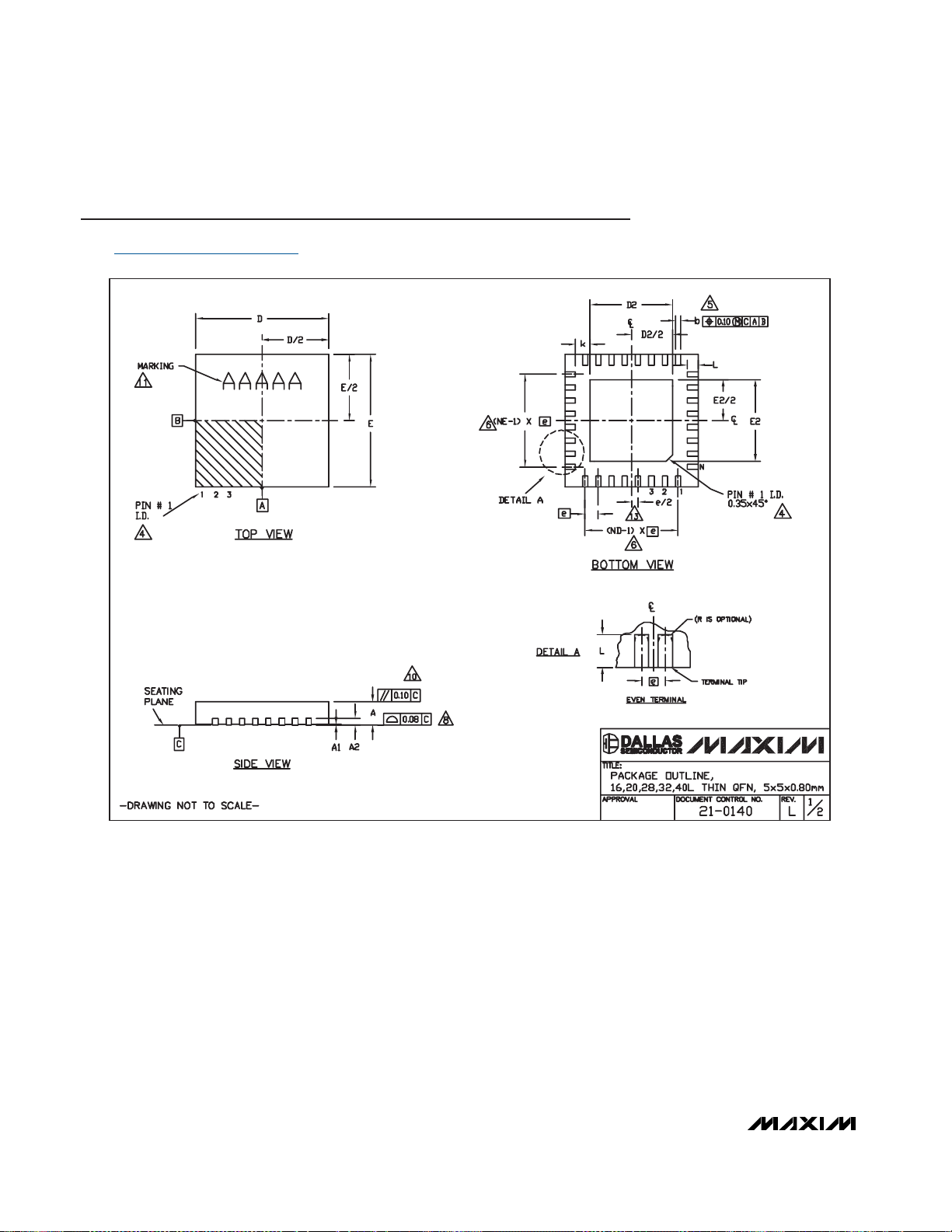
MAX3421E
USB Peripheral/Host Controller
with SPI Interface
28 ______________________________________________________________________________________
Package Information
(The package drawing(s) in this data sheet may not reflect the most current specifications. For the latest package outline information
go to www.maxim-ic.com/packages
.)
QFN THIN.EPS
Page 29

MAX3421E
USB Peripheral/Host Controller
with SPI Interface
______________________________________________________________________________________ 29
Package Information (continued)
(The package drawing(s) in this data sheet may not reflect the most current specifications. For the latest package outline information
go to www.maxim-ic.com/packages
.)
Page 30

MAX3421E
USB Peripheral/Host Controller
with SPI Interface
30 ______________________________________________________________________________________
Package Information (continued)
(The package drawing(s) in this data sheet may not reflect the most current specifications. For the latest package outline information
go to www.maxim-ic.com/packages
.)
32L TQFP, 5x5x01.0.EPS
B
1
2
21-0110
PACKAGE OUTLINE, 32L TQFP, 5x5x1.0mm
Page 31

MAX3421E
USB Peripheral/Host Controller
with SPI Interface
______________________________________________________________________________________ 31
Package Information (continued)
(The package drawing(s) in this data sheet may not reflect the most current specifications. For the latest package outline information
go to www.maxim-ic.com/packages
.)
B
2
2
21-0110
PACKAGE OUTLINE, 32L TQFP, 5x5x1.0mm
Page 32

MAX3421E
USB Peripheral/Host Controller
with SPI Interface
Maxim cannot assume responsibility for use of any circuitry other than circuitry entirely embodied in a Maxim product. No circuit patent licenses are
implied. Maxim reserves the right to change the circuitry and specifications without notice at any time.
32 ____________________Maxim Integrated Products, 120 San Gabriel Drive, Sunnyvale, CA 94086 408-737-7600
© 2007 Maxim Integrated Products is a registered trademark of Maxim Integrated Products. Inc.
Boblet
Revision History
REVISION
NUMBER
REVISION
DATE
DESCRIPTION
PAGES
CHANGED
3 7/07 Changes to pin description, addition of text 5, 25, 28–31
 Loading...