

Page 1
General Description
The MAX3397E ±15kV ESD-protected bidirectional
level translator provides level shifting for data transfer in
a multivoltage system. Externally applied voltages, V
CC
and VL, set the logic levels on either side of the device.
A logic-low signal present on the VLside of the device
appears as a logic-low signal on the VCCside of the
device, and vice versa. The MAX3397E utilizes a transmission-gate-based design to allow data translation in
either direction (VL↔ VCC) on any single data line. The
MAX3397E accepts VLfrom +1.2V to +5.5V and V
CC
from +1.65V to +5.5V, making the device ideal for data
transfer between low-voltage ASICs/PLDs and higher
voltage systems.
The MAX3397E features a shutdown mode that reduces
supply current to less than 1µA, thermal short-circuit protection, and ±15kV ESD protection on the VCCside for
greater protection in applications that route signals externally. The MAX3397E operates at a guaranteed data rate
of 8Mbps over the entire specified operating voltage
range. Within specific voltage domains, higher data rates
are possible. See the Timing Characteristics table.
The MAX3397E is available in an 8-pin µDFN package
and specified over the extended -40°C to +85°C operating temperature range.
Applications
Cell Phones, MP3 Players
Telecommunications Equipment
SPI™, MICROWIRE™, and I2C Level Translation
Portable POS Systems, Smart Card Readers
Low-Cost Serial Interfaces, GPS
Features
♦ Bidirectional Level Translation
♦ Guaranteed Data Rate
8Mbps (+1.2V ≤ V
L
≤ VCC≤ +5.5V)
16Mbps (+1.8V ≤ V
L
≤ VCC≤ +3.3V)
♦ Extended ESD Protection on the I/O VCCLines
±15kV Human Body Model
±15kV Air-Gap Discharge per IEC 61000-4-2
±8kV Contact Discharge per IEC 61000-4-2
♦ Enable/Shutdown
♦ Ultra-Low 1µA Supply Current in Shutdown Mode
♦ 8-Pin µDFN Package
MAX3397E
Dual Bidirectional Low-Level
Translator in µDFN
________________________________________________________________ Maxim Integrated Products 1
19-0771; Rev 0; 4/07
For pricing, delivery, and ordering information, please contact Maxim/Dallas Direct! at
1-888-629-4642, or visit Maxim’s website at www.maxim-ic.com.
EVALUATION KIT
AVAILABLE
Ordering Information
PART
TEMP
PINPACKAGE
TOP
PKG
CODE
MAX3397EELA+
-40°C to
8 µDFN
L822-1
Typical Application Circuit appears at end of data sheet.
SPI is a trademark of Motorola, Inc.
MICROWIRE is a trademark of National Semiconductor Corp.
+Denotes a lead-free package.
123
87465
MAX3397E
μDFN
(2mm x 2mm)
I/O V
CC1
VCCEN
+
I/O V
CC2
GND
V
L
I/O V
L2
I/O V
L1
Pin Configuration
RANGE
+85°C
(2mm x 2mm)
MARK
ABU
Page 2
MAX3397E
Dual Bidirectional Low-Level
Translator in µDFN
2 _______________________________________________________________________________________
ABSOLUTE MAXIMUM RATINGS
Stresses beyond those listed under “Absolute Maximum Ratings” may cause permanent damage to the device. These are stress ratings only, and functional
operation of the device at these or any other conditions beyond those indicated in the operational sections of the specifications is not implied. Exposure to
absolute maximum rating conditions for extended periods may affect device reliability.
(All voltages referenced to GND.)
V
CC
, VL.....................................................................-0.3V to +6V
I/O V
CC_
......................................................-0.3V to (VCC+ 0.3V)
I/O V
L_
..........................................................-0.3V to (VL+ 0.3V)
EN.............................................................................-0.3V to +6V
Short-Circuit Duration I/O V
L_
, I/O V
CC_
to GND .......Continuous
Continuous Power Dissipation (T
A
= +70°C)
8-Pin µDFN (derate 4.8mW/°C above +70°C) ............ 381mW
Operating Temperature Range ...........................-40°C to +85°C
Storage Temperature Range .............................-65°C to +150°C
Lead Temperature (soldering, 10s) .................................+300°C
ELECTRICAL CHARACTERISTICS
(VCC= +1.65V to +5.5V, VL= +1.2V to 5.5V, I/O VL_, and I/O V
CC_
are unconnected, TA= T
MIN
to T
MAX
, unless otherwise noted. Typical
values are at V
CC
= +3.3V, VL= +1.8V, TA = +25°C.) (Notes 1, 2)
PARAMETER SYMBOL CONDITIONS MIN
UNITS
POWER SUPPLIES
VL Supply Range V
L
1.2 5.5 V
VCC Supply Range V
CC
V
Supply Current from V
CC
I
QVCC
130 300 µA
Supply Current from V
L
I
QVL
110µA
VCC Shutdown-Mode Supply
Current
TA = +25°C, EN = GND
1µA
VL Shutdown-Mode Supply
Current
TA = +25°C, EN = GND
1µA
I/O VL_ and I/O V
CC_
Shutdown-
Mode Leakage Current
TA = +25°C, EN = GND
1µA
EN Input Leakage TA = +25°C
1µA
Tri-State Threshold Low V
TH_L
VCC falling (Note 3) 1.5 V
Tri-State Threshold High V
TH_H
VCC rising (Note 3) 1 V
ESD PROTECTION
I/O V
CC
Human Body Model (Note 4) ±15 kV
LOGIC-LEVEL THRESHOLDS
I/O VL_ Input-Voltage High V
IHL
VL -
0.2
V
I/O VL_ Input-Voltage Low V
ILL
V
I/O V
CC_
Input-Voltage High V
IHC
VCC -
0.4
V
I/O V
CC_
Input-Voltage Low V
ILC
V
I/O VL_ Output-Voltage High V
OHL
I/O VL_ source current = 20µA,
I/O V
CC_
> VCC - 0.4V
0.67 x
V
L
V
I/O VL_ Output-Voltage Low V
OLL
I/O VL_ sink current = 1mA,
I/O V
CC_
< 0.15V
0.4 V
TYP MAX
1.65 5.50
I
SHUTDOWN-VCC
I
SHUTDOWN-VL
I
SHUTDOWN-LKG
0.03
0.03
0.02
0.02
0.15
0.15
Page 3
MAX3397E
Dual Bidirectional Low-Level
Translator in µDFN
_______________________________________________________________________________________ 3
ELECTRICAL CHARACTERISTICS (continued)
(VCC= +1.65V to +5.5V, VL= +1.2V to 5.5V, I/O VL_, and I/O V
CC_
are unconnected, TA= T
MIN
to T
MAX
, unless otherwise noted. Typical
values are at V
CC
= +3.3V, VL= +1.8V, TA = +25°C.) (Notes 1, 2)
PARAMETER SYMBOL CONDITIONS MIN
TYP
MAX
UNITS
I/O V
CC_
Output-Voltage High V
OHC
I/O V
CC_
source current = 20µA,
I/O V
L _
> VL - 0.2V
0.67 x
V
CC
V
I/O V
CC_
Output-Voltage Low V
OLC
I/O V
CC_
sink current = 1mA,
I/O V
L_
< 0.15V
0.4 V
EN Input-Voltage High V
IH-EN
VL -
0.2
V
EN Input-Voltage Low V
IL-EN
V
RISE/FALL-TIME ACCELERATOR STAGE
I/O VCC side 0.8
Transition-Detect Threshold
I/O V
L
side 0.8
V
Accelerator Pulse Duration VL = 1.2V, VCC = 1.65V 27 ns
VL = 1.2V, VCC = 1.65V 40
I/O VL_ Output-Accelerator
Source Impedance
V
L
= 5V, VCC = 5V 9
Ω
VL = 1.2V, VCC = 1.65V 30
I/O V
CC_
Output-Accelerator
Source Impedance
V
L
= 5V, VCC = 5V 12
Ω
TIMING CHARACTERISTICS
(VCC= +1.65V to +5.5V, VL= +1.2V to +5.5V, R
LOAD
= 1MΩ, C
LOAD
= 15pF, driver output impedance ≤ 50Ω, I/O test signal of
Figure 1, T
A
= T
MIN
to T
MAX
, unless otherwise noted. Typical values are at VCC= +3.3V, VL= +1.8V, TA= +25°C.) (Notes 1, 2)
0.15
PARAMETER SYMBOL CONDITIONS MIN TYP MAX UNITS
+1.2V ≤ VL ≤ VCC ≤ +5.5V
I/O V
CC_
I/O V
CC_
I/O VL_ Rise Time t
I/O VL_ Fall Time t
Propagation Delay
Channel-to-Channel Skew t
Maximum Data Rate
Rise Time t
Fall Time t
Push-pull driving (Figure 1a) 7 25
Open-drain driving (Figure 1c) 170 400
Push-pull driving (Figure 1a) 6 37
Open-drain driving (Figure 1c) 6 37
Push-pull driving (Figure 1b) 8 30
Open-drain driving (Figure 1d) 180 400
Push-pull driving (Figure 1b) 3 30
Open-drain driving (Figure 1d) 3 30
Driving I/O V
Driving I/O V
Each translator
equally loaded
Push-pull driving 8 Mbps
Open-drain driving 500 kbps
t
PD-VL-VCC
t
PD-VCC-VL
RVCC
FVCC
RVL
FVL
SKEW
L_
CC_
Push-pull driving (Figure 1a) 5 30
Open-drain driving (Figure 1c) 170 800
Push-pull driving (Figure 1b) 4 30
Open-drain driving (Figure 1d) 190 1000
Push-pull driving 20
Open-drain driving 50
ns
ns
ns
ns
ns
ns
Page 4
MAX3397E
Dual Bidirectional Low-Level
Translator in µDFN
4 _______________________________________________________________________________________
Note 1: All units are 100% production tested at TA= +25°C. Limits over the operating temperature range are guaranteed by design
and not production tested.
Note 2: For normal operation, ensure VL< (V
CC
+ 0.3V).
Note 3: When V
CC
is below VLby more than the tri-state threshold, the device turns off its pullup resistors and I/O_ enters tri-state.
The device is not in shutdown.
Note 4: To ensure maximum ESD protection, place a 1µF capacitor between V
CC
and GND. See the Typical Application Circuit.
Note 5: 10% of input to 90% of output.
Note 6: 90% of input to 10% of output.
PARAMETER
CONDITIONS
UNITS
+1.8V ≤ VL ≤ VCC ≤ +3.3V
I/O V
CC_
Rise Time t
RVCC
Figure 1a (Note 5) 15 ns
I/O V
CC_
Fall Time t
FVCC
Figure 1a (Note 6) 15 ns
I/O VL_ Rise Time t
RVL
Figure 1b (Note 5) 15 ns
I/O VL_ Fall Time t
FVL
Figure 1b (Note 6) 15 ns
Driving I/O V
L_
15
Propagation Delay
Driving I/O V
CC_
15
ns
Channel-to-Channel Skew t
SKEW
Each translator equally loaded 10 ns
Maximum Data Rate 16
Mbps
TIMING CHARACTERISTICS (continued)
(VCC= +1.65V to +5.5V, VL= +1.2V to +5.5V, R
LOAD
= 1MΩ, C
LOAD
= 15pF, driver output impedance ≤ 50Ω, I/O test signal of
Figure 1, T
A
= T
MIN
to T
MAX
, unless otherwise noted. Typical values are at VCC= +3.3V, VL= +1.8V, TA= +25°C.) (Notes 1, 2)
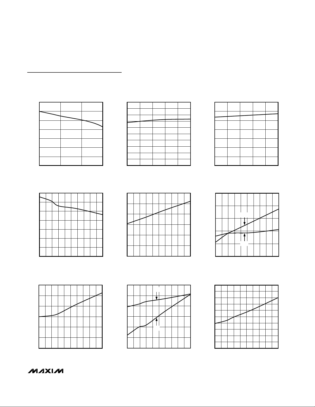
Typical Operating Characteristics
(VCC= +3.3V, VL= +1.8V, R
LOAD
= 1MΩ, C
LOAD
= 15pF, TA= +25°C, data rate = 8Mbps, unless otherwise noted.)
0
100
50
200
150
250
300
1.65 3.30 3.852.20 2.75 4.40 4.95 5.50
VL SUPPLY CURRENT vs. VCC SUPPLY VOLTAGE
(DRIVING ONE I/O V
L_
)
MAX3397E toc01
VCC SUPPLY VOLTAGE (V)
V
L
SUPPLY CURRENT (μA)
0
50
150
100
200
250
1.65 2.752.20 3.30 3.85 4.40 4.95 5.50
VL SUPPLY CURRENT vs. VCC SUPPLY VOLTAGE
(DRIVING ONE I/O V
CC_
)
MAX3397E toc02
VCC SUPPLY VOLTAGE (V)
V
L
SUPPLY CURRENT (μA)
0
300
100
200
500
400
700
600
800
1.2 1.9 2.6 3.3
VCC SUPPLY CURRENT vs. VL SUPPLY VOLTAGE
(DRIVING ONE I/O V
L_
)
MAX3397E toc03
VL SUPPLY VOLTAGE (V)
V
CC
SUPPLY CURRENT (μA)
SYMBOL
MIN TYP MAX
t
PD-VL-VCC
t
PD-VCC-VL
Page 5
MAX3397E
Dual Bidirectional Low-Level
Translator in µDFN
_______________________________________________________________________________________ 5
Typical Operating Characteristics (continued)
(VCC= +3.3V, VL= +1.8V, R
LOAD
= 1MΩ, C
LOAD
= 15pF, TA= +25°C, data rate = 8Mbps, unless otherwise noted.)
0
100
50
200
150
300
250
350
1.2 1.9 2.6 3.3
VCC SUPPLY CURRENT vs. VL SUPPLY VOLTAGE
(DRIVING ONE I/O V
CC_
)
MAX3397E toc04
VL SUPPLY VOLTAGE (V)
V
CC
SUPPLY CURRENT (μA)
0
60
40
20
80
100
120
140
160
180
200
-40 10-15 35 60 85
VL SUPPLY CURRENT vs. TEMPERATURE
(DRIVING ONE I/O V
L_
)
MAX3397E toc05
TEMPERATURE (°C)
V
L
SUPPLY CURRENT (μA)
0
100
50
200
150
300
250
350
-40 10-15 35 60 85
VL SUPPLY CURRENT vs. TEMPERATURE
(DRIVING ONE I/O V
CC_
)
MAX3397E toc06
TEMPERATURE (°C)
V
L
SUPPLY CURRENT (μA)
0
40
20
80
60
120
100
140
02010 30 4052515 35 45 50
VL SUPPLY CURRENT vs. CAPACITIVE LOAD
(DRIVING ONE I/O V
L_
)
MAX3397E toc07
CAPACITIVE LOAD (pF)
V
L
SUPPLY CURRENT (μA)
0
600
400
200
800
1000
1200
020155 10 253035404550
VCC SUPPLY CURRENT vs. CAPACITIVE LOAD
(DRIVING ONE I/O V
L_
)
MAX3397E toc08
CAPACITIVE LOAD (pF)
V
CC
SUPPLY CURRENT (μA)
0
5
10
15
20
25
0202510 155 3035404550
RISE/FALL TIME vs. CAPACITIVE LOAD
(DRIVING ONE I/O V
L_
)
MAX3397E toc09
CAPACITIVE LOAD (pF)
RISE/FALL TIME (ns)
t
FVCC
t
RVCC
0
6
4
2
8
10
12
020155 10 253035404550
PROPAGATION DELAY vs. CAPACITIVE LOAD
(DRIVING ONE I/O V
L_
)
MAX3397E toc10
CAPACITIVE LOAD (pF)
PROPAGATION DELAY (ns)
0
6
4
2
8
10
12
020155 10 253035404550
RISE/FALL TIME vs. CAPACITIVE LOAD
(DRIVING ONE I/O V
CC_
)
MAX3397E toc11
CAPACITIVE LOAD (pF)
RISE/FALL TIME (ns)
t
RVL
t
FVL
0
2
1
4
3
6
5
7
9
8
10
010152052530354540 50
PROPAGATION DELAY vs. CAPACITIVE LOAD
(DRIVING ONE I/O V
CC_
)
CAPACITIVE LOAD (pF)
PROPAGATION DELAY (ns)
MAX3397E toc12
Page 6

MAX3397E
Dual Bidirectional Low-Level
Translator in µDFN
6 _______________________________________________________________________________________
Detailed Description
The MAX3397E bidirectional, ESD-protected level
translator provides the level shifting necessary to allow
data transfer in a multivoltage system. Externally
applied voltages, VCCand VL, set the logic levels on
either side of the device. A logic-low signal present on
the V
L
side of the device appears as a logic-low signal
on the VCCside of the device, and vice versa. The
device uses a transmission-gate-based design (see the
Functional Diagram) to allow data translation in either
direction (VL↔ VCC) on any single data line. The
MAX3397E accepts VLfrom +1.2V to +5.5V and V
CC
from +1.65V to +5.5V, making the device ideal for data
transfer between low-voltage ASICs/PLDs and higher
voltage systems.
The MAX3397E features a shutdown mode that
reduces the supply current to less than 1µA, thermal
short-circuit protection, and ±15kV ESD protection on
the VCCside for greater protection in applications that
route signals externally. The device operates at a guaranteed data rate of 8Mbps over the entire specified
operating voltage range. Within specific voltage
domains, higher data rates are possible. See the
Timing Characteristics table.
Typical Operating Characteristics (continued)
(VCC= +3.3V, VL= +1.8V, R
LOAD
= 1MΩ, C
LOAD
= 15pF, TA= +25°C, data rate = 8Mbps, unless otherwise noted.)
RAIL-TO-RAIL DRIVING
(DRIVING ONE I/O V
L_
)
MAX3397E toc13
20ns/div
I/O V
L_
I/O V
CC_
1V/div
1V/div
EXITING SHUTDOWN MODE
MAX3397E toc14
2μs/div
I/O V
CC_
EN
2V/div
I/O V
L_
1V/div
1V/div
Pin Description
PIN
FUNCTION
1
Input/Output 2. Referenced to VCC.
2 GND Ground
3V
L
Logic-Input Voltage. The supply voltage range is +1.2V ≤ VL ≤ +5.5V. Bypass this supply with a 0.1µF capacitor
located as close as possible to the input.
4
Input/Output 2. Referenced to VL.
5
Input/Output 1. Referenced to VL.
6 EN Enable Input. Drive EN high to enable the device. Drive EN low to put the device in shutdown mode.
7V
CC
VCC Input Voltage. The supply voltage range is +1.65V ≤ VCC ≤ +5.5V. Bypass this supply with a 0.1µF capacitor
located as close as possible to the input. A 1µF ceramic capacitor is recommended for full ESD protection.
8
Input/Output 1. Referenced to VCC.
NAME
I/O V
CC2
I/O V
L2
I/O V
L1
I/O V
CC1
Page 7

MAX3397E
Dual Bidirectional Low-Level
Translator in µDFN
_______________________________________________________________________________________ 7
Level Translation
For proper operation, ensure that +1.65V ≤ VCC≤ +5.5V
and +1.2V ≤ V
L
≤ +5.5V. During power-up sequencing,
VL≥ (VCC+ 0.3V) does not damage the device. The
speed-up circuitry limits the maximum data rate for the
MAX3397E to 16Mbps. The maximum data rate also
depends heavily on the load capacitance (see the
Typical Operating Characteristics), output impedance of
the driver, and the operational voltage range (see the
Timing Characteristics table).
Rise-Time Accelerators
The MAX3397E has an internal rise-time accelerator,
allowing operation up to 16Mbps. The rise-time accelerators are present on both sides of the device and act to
speed up the rise time of the input and output of the
device, regardless of the direction of the data. The triggering mechanism for these accelerators is both level
and edge sensitive. To prevent false triggering of the
rise-time accelerators, signal fall times of less than
20ns/V are recommended for both the inputs and outputs
of the device. Under less noisy conditions, longer signal
fall times are acceptable. Note: To guarantee operation
of the rise time, accelerators the maximum parasitic
capacitance should be less than 200pF on the I/O lines.
Shutdown Mode
Drive EN low to place the MAX3397E in shutdown
mode. Connect EN to VLor VCC(logic-high) for normal
operation. Activating the shutdown mode disconnects
the internal 10kΩ pullup resistors on the I/O VCCand
I/O VLlines. This forces the I/O lines to a high-impedance state, and decreases the supply current to less
than 1µA. The high-impedance I/O lines in shutdown
mode allow for use in a multidrop network. The
MAX3397E effectively has a diode from each I/O to the
corresponding supply rail and GND. Therefore, when in
shutdown mode, do not allow the voltage at I/O VL_to
exceed (VL+ 0.3V), or the voltage at I/O V
CC_
to
exceed (VCC+ 0.3V).
MAX3397E
I/O VL_
I/O V
CC
_
(t
RISE
,
t
FALL
< 10ns)
DATA
I/O V
CC
_
V
CC
V
CC
V
L
GND
R
LOAD
C
LOAD
t
PD-VCC-VL
t
PD-VCC-VL
I/O VL_
t
RVL
t
FVL
EN
V
L
Figure 1a. Rail-to-Rail Driving I/O V
L
Figure 1b. Rail-to-Rail Driving I/O V
CC
I/O V
L
,
(t
RISE
< 10ns)
t
FALL
I/O VCC_
V
L
V
V
CC
L
EN
MAX3397E
I/O VL_
_
t
PD-VL-VCC
t
RVCC
I/O V
GND
V
CC
DATA
_
CC
R
LOAD
t
PD-VL-VCC
t
FVCC
C
LOAD
Page 8

MAX3397E
Dual Bidirectional Low-Level
Translator in µDFN
8 _______________________________________________________________________________________
Operation with One Supply Disconnected
Certain applications require sections of circuitry to be
disconnected to save power. When V
L
is connected and
VCCis disconnected or connected to ground, the device
enters shutdown mode. In this mode, I/O VLcan still be
driven without damage to the device; however, data
does not translate from I/O V
L
to I/O VCC. If VCCfalls
more than 0.8V (typ) below V
L
, the device disconnects
the pullup resistors at I/O VLand I/O VCC. To achieve
the lowest possible supply current from VLwhen VCCis
disconnected, it is recommended that the voltage at the
V
CC
supply input be approximately equal to GND. Note:
When V
CC
is disconnected or connected to ground, I/O
VCCmust not be driven more than VCC+ 0.3V.
When VCCis connected and VLis less than 0.7V (typ),
the device enters shutdown mode. In this mode, I/O
VCCcan still be driven without damage to the device;
however, data does not translate from I/O VCCto I/O VL.
Note: When V
L
is disconnected or connected to
ground, I/O V
L
must not be driven more than VL+ 0.3V.
Thermal Short-Circuit Protection
Thermal-overload detection protects the MAX3397E
from short-circuit fault conditions. In the event of a
short-circuit fault, when the junction temperature (T
J
)
reaches +150°C, a thermal sensor signals the shutdown mode logic to force the device into shutdown
mode. When the T
J
has cooled to +140°C, normal
operation resumes.
±15kV ESD Protection
As with all Maxim devices, ESD-protection structures
are incorporated on all pins to protect against electrostatic discharges encountered during handling and
assembly. The I/O VCClines have extra protection
against static electricity. Maxim’s engineers have
developed state-of-the-art structures to protect these
pins against ESD of ±15kV without damage. The ESD
structures withstand high ESD in all states: normal
operation, shutdown mode, and powered down. After
an ESD event, Maxim’s E versions keep working without
MAX3397E
I/O V
L_
I/O V
CC_
DATA
I/O V
CC_
V
CC
V
CC
V
L
GND
R
LOAD
C
LOAD
t
PD-VCC-VL
t
PD-VCC-VL
I/O V
L_
t
RVL
t
FVL
EN
V
L
Figure 1c. Open-Drain Driving I/O V
L
Figure 1d. Open-Drain Driving I/O V
CC
V
L
I/O V
L_
t
PD-VL-VCC
I/O V
CC_
t
RVCC
EN
I/O V
L_
V
V
L
MAX3397E
GND
V
CC
CC
DATA
I/O V
CC_
t
PD-VL-VCC
t
FVCC
C
R
LOAD
LOAD
Page 9

MAX3397E
Dual Bidirectional Low-Level
Translator in µDFN
_______________________________________________________________________________________ 9
latchup, whereas competing products can latch and
must be powered down to remove latchup. ESD protection can be tested in various ways. The I/O VCClines of
the MAX3397E are characterized for protection to the
following limits:
1) ±15kV using the Human Body Model
2) ± 8kV using the Contact Discharge method specified
by IEC 61000-4-2
3) ±15kV using the Air-Gap Discharge method specified
by IEC 61000-4-2
ESD Test Conditions
ESD performance depends on a variety of conditions.
Contact Maxim for a reliability report that documents
test setup, test methodology, and test results.
Human Body Model
Figure 2a shows the Human Body Model, and Figure 2b
shows the current waveform it generates when discharged into a low-impedance state. This model consists of a 100pF capacitor charged to the ESD voltage
of interest that is then discharged into the test device
through a 1.5kΩ resistor.
IEC 61000-4-2
The IEC 61000-4-2 standard covers ESD testing and
performance of finished equipment; it does not specifically refer to integrated circuits. The MAX3397E helps
I/O V
L_
PU1
GATE
BIAS
N
V
L
ONE-SHOT
BLOCK
TRIGGER
I/O V
CC_
PU2
V
CC
EN
ONE-SHOT
BLOCK
GND
MAX3397E
Functional Diagram
IP 100%
90%
36.8%
t
RL
TIME
t
DL
CURRENT WAVEFORM
PEAK-TO-PEAK RINGING
(NOT DRAWN TO SCALE)
I
r
10%
0
0
AMPERES
Figure 2b. Human Body Current Waveform
CHARGE-CURRENT-
LIMIT RESISTOR
DISCHARGE
RESISTANCE
STORAGE
CAPACITOR
C
s
100pF
R
C
1MΩ RD 1500Ω
HIGH-
VOLTAGE
DC
SOURCE
DEVICE
UNDER
TEST
Figure 2a. Human Body ESD Test Model
Page 10

MAX3397E
Dual Bidirectional Low-Level
Translator in µDFN
10 ______________________________________________________________________________________
to design equipment that meets Level 4 of IEC 610004-2 without the need for additional ESD-protection components.
The major difference between tests done using the
Human Body Model and IEC 61000-4-2 is higher peak
current in IEC 61000-4-2 because series resistance is
lower in the IEC 61000-4-2 model. Hence, the ESD
withstand voltage measured to IEC 61000-4-2 is generally lower than that measured using the Human Body
Model. Figure 3a shows the IEC 61000-4-2 model, and
Figure 3b shows the current waveform for the ±8kV,
IEC 61000-4-2, Level 4, ESD contact-discharge test.
The Air-Gap test involves approaching the device with a
charged probe. The contact-discharge method connects
the probe to the device before the probe is energized.
Machine Model
The Machine Model for ESD tests all pins using a
200pF storage capacitor and zero discharge resistance. Its objective is to emulate the stress caused by
contact that occurs with handling and assembly during
manufacturing. Of course, all pins require this protection during manufacturing, not just inputs and outputs.
Therefore, after PCB assembly, the Machine Model is
less relevant to I/O ports.
Applications Information
Power-Supply Decoupling
To reduce ripple and the chance of transmitting incorrect
data, bypass VLand VCCto ground with a 0.1µF capacitor (see the Typical Application Circuit). To ensure full
±15kV ESD protection, bypass VCCto ground with a 1µF
capacitor. Place all capacitors as close as possible to
the power-supply inputs.
I2C Level Translation
The MAX3397E level-shifts the data present on the I/O
lines between +1.2V and +5.5V, making them ideal for
level translation between a low-voltage ASIC and an
I2C device. A typical application involves interfacing a
low-voltage microprocessor to a 3V or 5V D/A converter, such as the MAX517.
Push-Pull vs. Open-Drain Driving
The MAX3397E can be driven in a push-pull configuration and include internal 10kΩ resistors that pull up I/O
VL_and I/O V
CC_
to their respective power supplies,
allowing operation of the I/O lines with open-drain
devices. See the Timing Characteristics table for maximum data rates when using open-drain drivers.
Chip Information
PROCESS: BiCMOS
tr = 0.7ns to 1ns
30ns
60ns
t
100%
90%
10%
I
PEAK
I
Figure 3b. IEC 61000-4-2 ESD Generator Current Waveform
CHARGE-CURRENT-
LIMIT RESISTOR
DISCHARGE
RESISTANCE
STORAGE
CAPACITOR
C
s
150pF
R
C
50MΩ to 100MΩ RD 330Ω
HIGH-
VOLTAGE
DC
SOURCE
DEVICE
UNDER
TEST
Figure 3a. IEC 61000-4-2 ESD Test Model
Page 11

MAX3397E
Dual Bidirectional Low-Level
Translator in µDFN
______________________________________________________________________________________ 11
MAX3397E
EN
I/O V
L2
I/O V
L1
DATADATA
I/O V
CC2
I/O V
CC1
0.1μF0.1μF 1μF
+3.3V+1.8V
V
CC
+3.3V
SYSTEM
+1.8V
SYSTEM
CONTROLLER
V
L
Typical Application Circuit
Page 12

MAX3397E
Dual Bidirectional Low-Level
Translator in µDFN
12 ______________________________________________________________________________________
Package Information
(The package drawing(s) in this data sheet may not reflect the most current specifications. For the latest package outline information,
go to www.maxim-ic.com/packages
.)
6, 8, 10L UDFN.EPS
EVEN TERMINAL
L
C
ODD TERMINAL
L
C
L
e
L
A
e
E
D
PIN 1
INDEX AREA
b
e
A
b
N
SOLDER
MASK
COVERAGE
A A
1
PIN 1
0.10x45∞
L
L1
(N/2 -1) x e)
XXXX
XXXX
XXXX
SAMPLE
MARKING
A1
A2
7
A
1
2
21-0164
PACKAGE OUTLINE,
6, 8, 10L uDFN, 2x2x0.80 mm
-DRAWING NOT TO SCALE-
Page 13

MAX3397E
Dual Bidirectional Low-Level
Translator in µDFN
Maxim cannot assume responsibility for use of any circuitry other than circuitry entirely embodied in a Maxim product. No circuit patent licenses are
implied. Maxim reserves the right to change the circuitry and specifications without notice at any time.
Maxim Integrated Products, 120 San Gabriel Drive, Sunnyvale, CA 94086 408-737-7600 ____________________ 13
© 2007 Maxim Integrated Products is a registered trademark of Maxim Integrated Products, Inc.
Springer
Package Information (continued)
(The package drawing(s) in this data sheet may not reflect the most current specifications. For the latest package outline information,
go to www.maxim-ic.com/packages
.)
COMMON DIMENSIONS
SYMBOL MIN. NOM.
A
0.70 0.75
A1
D 1.95 2.00
E
1.95 2.00
L
0.30 0.40
PKG. CODE N e b
PACKAGE VARIATIONS
L1
6L622-1 0.65 BSC 0.30±0.05
0.25±0.050.50 BSC8L822-1
0.20±0.030.40 BSC10L1022-1
2.05
0.80
MAX.
0.50
2.05
0.10 REF.
(N/2 -1) x e
1.60 REF.
1.50 REF.
1.30 REF.
A2
-
-DRAWING NOT TO SCALE-
A
2
2
21-0164
PACKAGE OUTLINE,
6, 8, 10L uDFN, 2x2x0.80 mm
0.15 0.20 0.25
0.020 0.025 0.035
 Loading...