

Page 1
General Description
The MAX3394E/MAX3395E/MAX3396E bidirectional
level translators provide level shifting required for data
transfer in a multivoltage system. Internal slew-rate
enhancement circuitry features 10mA current-sink and
15mA current-source drivers to isolate capacitive loads
from lower current drivers. In open-drain systems, slewrate enhancement enables fast data rates with larger
pullup resistors and increased bus load capacitance.
Externally applied voltages, V
CC
and VL, set the logichigh levels for the device. A logic-low signal on one I/O
side of the device appears as a logic-low signal on the
opposite I/O side, and vice-versa. Each I/O line is
pulled up to V
CC
or VLby an internal pullup resistor,
allowing the devices to be driven by either push-pull or
open-drain drivers.
The MAX3394E/MAX3395E/MAX3396E feature a tristate output mode, thermal-shutdown protection, and
±15kV Human Body Model (HBM) ESD protection on
the VCCside for greater protection in applications that
route signals externally.
The MAX3394E/MAX3395E/MAX3396E accept V
CC
volt-
ages from +1.65V to +5.5V, and V
L
voltages from +1.2V
to V
CC
, making them ideal for data transfer between low
voltage ASIC/PLDs and higher voltage systems. The
MAX3394E/MAX3395E/MAX3396E operate at a guaranteed data rate of 6Mbps with push-pull drivers and
1Mbps with open-drain drivers.
The MAX3394E is a dual-level translator available in
9-bump UCSP™ and 8-pin 3mm x 3mm TDFN packages.
The MAX3395E is a quad-level translator available in 12bump UCSP, and 12-pin 4mm x 4mm TQFN packages.
The MAX3396E is an octal-level translator available in 20bump UCSP and 20-pin 5mm x 5mm TQFN packages.
The MAX3394E/MAX3395E/MAX3396E operate over the
extended -40°C to +85°C temperature range.
Applications
Multivoltage Bidirectional Level Translation
SPI™, MICROWIRE™, and I2C Level Translation
Open-Drain Rise-Time Speed-Up
High-Speed Bus Fan-Out Expansion
Cell Phones
Telecom, Networking, Servers, RAID/SAN
Features
♦ ±15kV ESD Protection on I/O V
CC_
Lines
♦ Bidirectional Level Translation Without Direction
Pin
♦ I/O V
L_
and I/O V
CC_
10mA Sink-/15mA Source-
Current Capability
♦ Slew-Rate Enhancement Circuitry Supports
Larger Capacitive Loads or Larger External Pullup
Resistors
♦ 6Mbps Push-Pull/1Mbps Open-Drain Guaranteed
Data Rate
♦ Wide Supply-Voltage Range: Operation Down to
+1.2V on V
L
and +1.65V on V
CC
♦ Low Supply Current in Tri-State Output Mode
(3µA typ)
♦ Low Quiescent Current
♦ Thermal-Shutdown Protection
♦ UCSP, TDFN, and TQFN Packages
MAX3394E/MAX3395E/MAX3396E
±15kV ESD-Protected, High-Drive Current, Dual-/Quad-/
Octal-Level Translators with Speed-Up Circuitry
________________________________________________________________
Maxim Integrated Products
1
19-3884; Rev 2; 2/07
For pricing, delivery, and ordering information, please contact Maxim/Dallas Direct! at
1-888-629-4642, or visit Maxim’s website at www.maxim-ic.com.
12
34
8
7
6
5
V
L
I/O V
L
1
I/O V
L
2
GND
*CONNECT EXPOSED PAD TO GROUND
*EP
I/O V
CC
2
I/O V
CC
1
EN
V
CC
MAX3394E
TDFN
TOP VIEW
(LEADS ON BOTTOM)
+
Pin Configurations
Ordering Information
MICROWIRE is a trademark of National Semiconductor Corp.
SPI is a trademark of Motorola, Inc.
UCSP is a trademark of Maxim Integrated Products, Inc.
Note: All devices specified over the -40°C to +85°C operating
range.
+
Denotes lead(Pb)-free/RoHS-compliant package.
*
Future product—contact factory for availability.
**EP = Exposed paddle.
Pin Configurations continued at end of data sheet.
Selector Guide appears at end of data sheet.
PART PIN-PACKAGE PKG CODE
MAX3394EETA+T 8 TDFN-EP** T833-1
MAX3394EEBL+T 9 UCSP B9-5
MAX3395EETC+ 12 TQFN-EP** T1244-4
MAX3395EEBC+T 12 UCSP B12-1
MAX3396EEBP+T* 20 UCSP B20-1
MAX3396EETP+* 20 TQFN-EP** T2055-4
Page 2
MAX3394E/MAX3395E/MAX3396E
±15kV ESD-Protected, High-Drive Current, Dual-/Quad-/
Octal-Level Translators with Speed-Up Circuitry
2 _______________________________________________________________________________________
ABSOLUTE MAXIMUM RATINGS
Stresses beyond those listed under “Absolute Maximum Ratings” may cause permanent damage to the device. These are stress ratings only, and functional
operation of the device at these or any other conditions beyond those indicated in the operational sections of the specifications is not implied. Exposure to
absolute maximum rating conditions for extended periods may affect device reliability.
(All voltages referenced to GND.)
V
CC
......................................................................... -0.3V to +6V
V
L
............................................................................ -0.3V to +6V
I/O V
CC_
...................................................... -0.3V to VCC+ 0.3V
I/O V
L_
........................................................... -0.3V to VL+ 0.3V
EN ........................................................................... -0.3V to +6V
Short-Circuit Duration I/O V
L_
, I/O V
CC_
to GND ..... Continuous
Maximum Continuous Current ........................................ ±50mA
Continuous Power Dissipation (T
A
= +70°C)
8-Pin TDFN (derate 18.2mW/°C above +70°C) ........ 1455mW
9-Bump UCSP (derate 4.7mW/°C above +70°C) ........ 379mW
12-Pin TQFN (derate 16.9mW/°C above +70°C) ........1349mW
12-Bump UCSP (derate 6.5mW/°C above +70°C) ..... 519mW
20-Pin TQFN (derate 20.8mW/°C above +70°C) ........1667mW
20-Bump UCSP (derate 10.0mW/°C above +70°C) .....800mW
Operating Temperature Range ......................... -40°C to +85°C
Storage Temperature Range ........................... -65°C to +150°C
Junction Temperature .....................................................+150°C
Bump Temperature (soldering) ...................................... +235°C
Lead Temperature (soldering, 10s) ............................... +300°C
ELECTRICAL CHARACTERISTICS
(VCC= +1.65V to +5.5V, VL= +1.2V to VCC; C
IOVL
≤ 15pF, C
IOVCC
≤ 15pF; TA= -40°C to +85°C, unless otherwise noted. Typical val-
ues are at T
A
= +25°C.) (Note 1)
POWER SUPPLY
VL Supply Range V
VCC Supply Range V
Supply Current from V
VCC Tri-State Supply Current I
VL Tri-State Supply Current I
LOGIC I/O
I/O VL_ Input-Voltage High
Threshold
I/O VL_ Input-Voltage Low
Threshold
I/O VL_ Internal Pullup DC
Resistance
I/O VL_ Source Current During
Low-to-High Transition
I/O VL_ Sink Current During Highto-Low Transition
PARAMETER SYMBOL CONDITIONS MIN TYP MAX UNITS
CC
CC
L
I
CC
I
L
CC-3
L-3
V
IHL
V
ILL
R
I
IHL
I
ILL
L
I/O lines internally
pulled up
I/O lines internally
pulled up
EN = GND, TA = +25°C 3 6 µA
EN = GND, TA = +25°C 0.7 2 µA
EN = VCC or V
L
VL = +1.2V 15 mA
V
CC
= +1.65V 10 mA
1.2 V
1.65 5.50 V
MAX3394E 150
MAX3395E 300Supply Current from V
MAX3396E 600
MAX3394E 30
MAX3395E 30
MAX3396E 30
0.3 x
V
L
L
51020kΩ
CC
0.7 x
V
L
V
µA
µA
V
V
Page 3
MAX3394E/MAX3395E/MAX3396E
±15kV ESD-Protected, High-Drive Current, Dual-/Quad-/
Octal-Level Translators with Speed-Up Circuitry
_______________________________________________________________________________________ 3
ELECTRICAL CHARACTERISTICS (continued)
(VCC= +1.65V to +5.5V, VL= +1.2V to VCC; C
IOVL
≤ 15pF, C
IOVCC
≤ 15pF; TA= -40°C to +85°C, unless otherwise noted. Typical val-
ues are at T
A
= +25°C.) (Note 1)
I/O VL_ Low-to-High Transition
Threshold
I/O VL_ Output-Voltage Low V
PARAMETER SYMBOL CONDITIONS MIN TYP MAX UNITS
V
L-TH
OLL
I/O VL_ Tri-State Output Leakage
Current
I/O VCC_ Input-Voltage High
Threshold
I/O VCC_ Input-Voltage Low
Threshold
I/O VCC_ Internal Pullup DC
Resistance
I/O VCC_ Source Current During
Low-to-High Transition
I/O VCC_ Sink Current During
High-to-Low Transition
I/O VCC_ Low-to-High Transition
Threshold
I/O VCC_ Output-Voltage Low V
V
V
R
I
IHCC
I
ILCC
V
CC-TH
IHC
ILC
CC
OLC
I/O VCC_ Tri-State Output
Leakage Current
EN Input-Voltage High Threshold V
EN Input-Voltage Low Threshold V
IHE
ILE
EN Pin Input Leakage Current TA = +25°C -1 +1 µA
ESD PROTECTION
I/O VCC_ ESD Protection C
V
= +3.3V, VL = +1.8V
CC
I/O VL_ sink current = 5mA, V
I/O VL_ sink current = 10mA, V
0.2 x V
L
EN = GND, T
= +25°C -1 +1 µA
A
(Note 2)
(Note 2)
EN = VCC or V
V
= +1.65V 15 mA
CC
V
= +1.65V 10 mA
CC
V
= +3.3V, VL = +1.8V
CC
L
I/O VCC_ sink current = 5mA, V
I/O VCC_ sink current = 10mA, V
or 0.2 x V
EN = GND, T
L
= +25°C -1 +1 µA
A
= 1µF, Human Body Model ±15 kV
VCC
0.3 x
V
= 0V 0.25
ILC
≤ 0.4V or
ILC
0.5 x
L
V
L
0.3 x
V
CC
51020kΩ
0.3 x
V
= 0V 0.25
ILL
≤ 0.4V
ILL
CC
0.5 x
V
CC
0.3 x
V
L
V
ILC
0.4V
0.7 x
V
V
ILL
0.4V
0.7 x
V
+
CC
+
L
V
V
V
V
V
V
V
V
Page 4
MAX3394E/MAX3395E/MAX3396E
±15kV ESD-Protected, High-Drive Current, Dual-/Quad-/
Octal-Level Translators with Speed-Up Circuitry
4 _______________________________________________________________________________________
TIMING CHARACTERISTICS
(VCC= +1.65V to +5.5V, VL= +1.2V to VCC; C
IOVL
≤ 15pF, C
IOVCC
≤ 15pF; TA= -40°C to +85°C, unless otherwise noted. Typical val-
ues are at T
A
= +25°C.) (Note 1)
Note 1: All units are 100% production tested at TA= +25°C. Limits over the operating temperature range are guaranteed by design
and not production tested.
Note 2: During a low-to-high transition, the threshold at which the I/O changes state is the lower of V
ILL
and V
ILC
since the two sides
are internally connected by an internal switch while the device is in the logic-low state.
I/O VCC_ Rise Time t
I/O VCC_ Fall Time t
I/O VL_ Rise Time t
I/O VL_ Fall Time t
Propagation Delay
Propagation Delay After EN t
Channel-to-Channel Skew t
Maximum Data Rate
PARAMETER SYMBOL CONDITIONS MIN TYP MAX UNITS
RVCC
FVCC
RVL
FVL
t
I/OVL-VCC
t
I/OVCC-VL
EN
SKEW
Push-pull driver, Figure 1 50
Open-drain driver, internal pullup, Figure 2 500
Push-pull driver, Figure 1 50
Open-drain driver, internal pullup, Figure 2 50
Push-pull driver, Figure 3 50
Open-drain driver, internal pullup, Figure 4 500
Push-pull driver, Figure 3 50
Open-drain driver, internal pullup, Figure 4 50
Push-pull driver, Figure 1 50
Open-drain driver, internal pullup, Figure 2 600
Push-pull driver, Figure 3 50
Open-drain driver, internal pullup, Figure 4 600
Push-pull or open-drain driver, Figure 5 5 µs
Push-pull driver 5
Open-drain driver, internal pullup 100
Push-pull driver, Figures 1, 3 6
Open-drain driver, internal pullup,
Figures 2, 4
1
ns
ns
ns
ns
ns
ns
Mbps
Page 5
MAX3394E/MAX3395E/MAX3396E
±15kV ESD-Protected, High-Drive Current, Dual-/Quad-/
Octal-Level Translators with Speed-Up Circuitry
_______________________________________________________________________________________
5
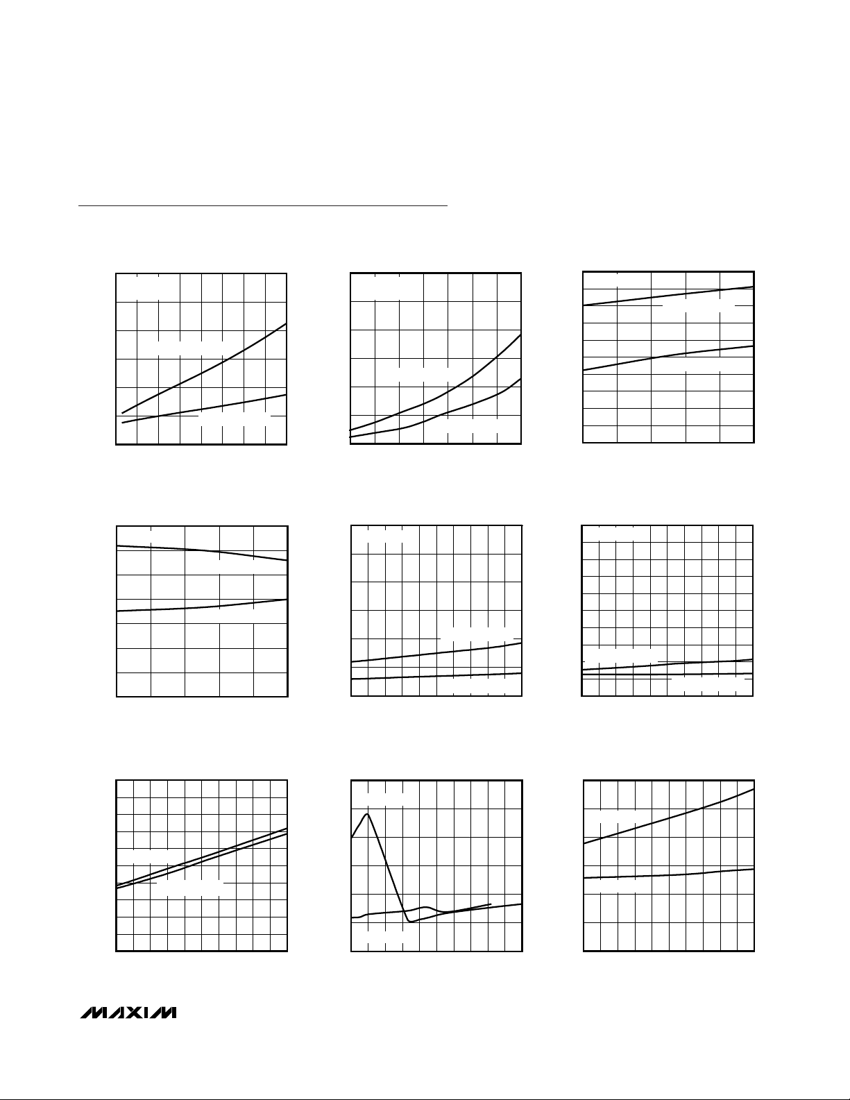
Typical Operating Characteristics
(VCC= +2.5V, VL= +1.8V, CL= 15pF, TA= +25°C, unless otherwise noted.)
VCC SUPPLY CURRENT
vs. SUPPLY VOLTAGE
MAX3394E–96E toc01
VCC SUPPLY VOLTAGE (V)
V
CC
SUPPLY CURRENT (mA)
5.04.54.03.53.02.52.0
0.5
1.0
1.5
2.0
2.5
3.0
0
1.5 5.5
VL = +1.2V
DRIVING I/O V
L_
1Mbps OPEN-DRAIN
6Mbps PUSH-PULL
VL SUPPLY CURRENT
vs. SUPPLY VOLTAGE
MAX3394E–96E toc02
VL SUPPLY VOLTAGE (V)
V
L
SUPPLY CURRENT (mA)
4.54.03.53.02.52.0
0.5
1.0
1.5
2.0
2.5
3.0
0
1.5 5.0
VCC = +5.0V
DRIVING I/O V
L_
1Mbps OPEN-DRAIN
6Mbps PUSH-PULL
VCC SUPPLY CURRENT
vs. TEMPERATURE
MAX3394E–96E toc03
TEMPERATURE (°C)
V
CC
SUPPLY CURRENT (mA)
603510-15
0.1
0.2
0.3
0.4
0.5
0.6
0.7
0.8
0.9
1.0
0
-40 85
DRIVING I/O V
L_
1Mbps OPEN-DRAIN
6Mbps PUSH-PULL
VL SUPPLY CURRENT
vs. TEMPERATURE
MAX3394E–96E toc04
TEMPERATURE (°C)
V
L
SUPPLY CURRENT (mA)
603510-15
0.05
0.10
0.15
0.20
0.25
0.30
0.35
0
-40 85
DRIVING I/O V
L_
1Mbps OPEN-DRAIN
6Mbps PUSH-PULL
0
1.5
1.0
0.5
2.0
2.5
3.0
0403010 20 50 60 70 80 90 100
MAX3394E-96E toc05
LOAD CAPACITANCE (pF)
V
CC
SUPPLY CURRENT (mA)
VCC SUPPLY CURRENT
vs. LOAD CAPACITANCE
DRIVING I/O V
L_
6Mbps PUSH-PULL
1Mbps OPEN-DRAIN
0
0.2
0.1
0.4
0.3
0.6
0.5
0.7
0.9
0.8
1.0
020304010 50 60 70 9080 100
MAX3394E-96E toc06
LOAD CAPACITANCE (pF)
V
L
SUPPLY CURRENT (mA)
VL SUPPLY CURRENT
vs. LOAD CAPACITANCE
DRIVING I/O V
L_
6Mbps PUSH-PULL
1Mbps OPEN-DRAIN
0
100
50
200
150
300
250
350
450
400
500
020304010 50 60 70 9080 100
MAX3394E-96E toc07
CAPACITIVE LOAD (pF)
RISE TIME (ns)
OPEN-DRAIN RISE TIME
vs. LOAD CAPACITANCE
DRIVING I/O V
L_
DRIVING I/O V
CC_
OPEN-DRAIN FALL TIME
vs. LOAD CAPACITANCE
MAX3394E–96E toc08
LOAD CAPACITANCE (pF)
FALL TIME (ns)
908070605040302010
5
10
15
20
25
30
0
0 100
DRIVING I/O V
CC_
DRIVING I/O V
L_
PUSH-PULL RISE TIME
vs. LOAD CAPACITANCE
MAX3394E–96E toc09
LOAD CAPACITANCE (pF)
RISE TIME (ns)
908070605040302010
5
10
15
20
25
30
0
0 100
DRIVING I/O V
CC_
DRIVING I/O V
L_
Page 6
MAX3394E/MAX3395E/MAX3396E
±15kV ESD-Protected, High-Drive Current, Dual-/Quad-/
Octal-Level Translators with Speed-Up Circuitry
6 _______________________________________________________________________________________
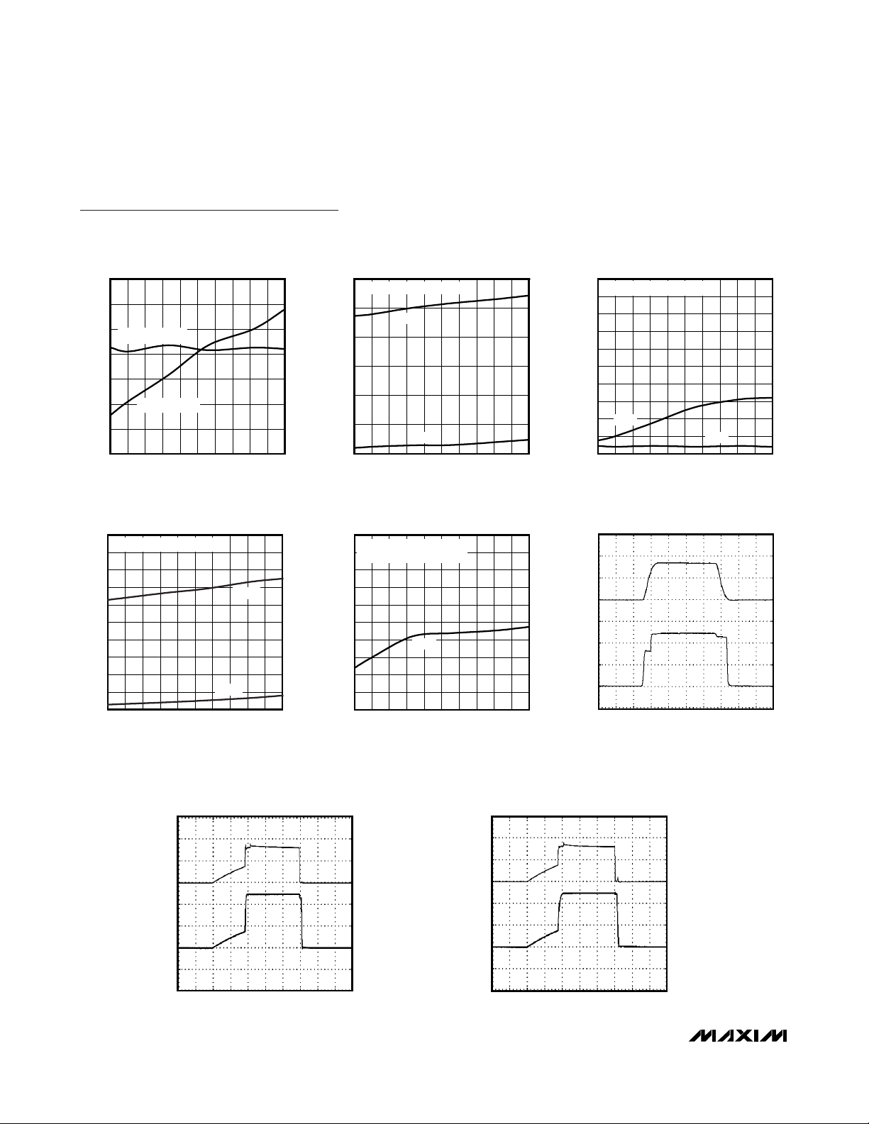
Typical Operating Characteristics (continued)
(VCC= +2.5V, VL= +1.8V, CL= 15pF, TA= +25°C, unless otherwise noted.)
0
4
2
8
6
12
10
14
04020 60 8010 5030 70 90 100
MAX3394E-96E toc10
LOAD CAPACITANCE (pF)
FALL TIME (ns)
PUSH-PULL FALL TIME
vs. LOAD CAPACITANCE
DRIVING I/O V
L_
DRIVING I/O V
CC_
0
15
10
5
20
25
30
0403010 20 50 60 70 80 90 100
PROPAGATION DELAY
vs. LOAD CAPACITANCE
MAX3394E-96E toc11
LOAD CAPACITANCE (pF)
PROPAGATIN DELAY (ns)
DRIVING I/O V
L_
OPEN-DRAIN
t
PDHL
t
PDLH
0
4
2
8
6
12
10
14
18
16
20
020304010 50 60 70 9080 100
MAX3394E-96E toc12
LOAD CAPACITANCE (pF)
PROPAGATION DELAY (ns)
DRIVING I/O V
CC_
OPEN-DRAIN
PROPAGATION DELAY
vs. LOAD CAPACITANCE
t
PDHL
t
PDLH
PROPAGATION DELAY
vs. LOAD CAPACITANCE
MAX3394E–96E toc13
LOAD CAPACITANCE (pF)
PROPAGATION DELAY (ns)
908060 7020 30 40 5010
5
10
15
20
25
30
35
40
45
50
0
0 100
t
PDHL
DRIVING I/O V
L_
PUSH-PULL
t
PDLH
0
4
2
8
6
12
10
14
18
16
20
020304010 50 60 70 9080 100
MAX3394E-96E toc14
LOAD CAPACITANCE (pF)
PROPAGATION DELAY (ns)
DRIVING I/O V
CC_
PUSH-PULL
SEE FIGURE 3
PROPAGATION DELAY
vs. LOAD CAPACITANCE
t
PDHL
40ns/div
(DRIVING I/O VL_, VCC = +2.5V, VL = +1.8V,
C
L
= 15pF, DATA RATE = 6Mbps)
I/O V
CC_
1V/div
I/O V
L_
1V/div
MAX3394E-96E toc15
200ns/div
(DRIVING I/O VL_, V
CC
= +5.0V, VL = +3.3V,
C
L
= 100pF, DATA RATE = 1Mbps)
MAX3394E-96E toc16
I/O V
CC_
2V/div
I/O V
L_
2V/div
200ns/div
(DRIVING I/O VL_, V
CC
= +5.0V, VL = +3.3V,
C
L
= 400pF, EXTERNAL 4.7kΩ
PULLUPS, DATA RATE = 1Mbps)
MAX3394E-96E toc17
I/O V
CC_
2V/div
I/O V
L_
2V/div
Page 7

Detailed Description
The MAX3394E/MAX3395E/MAX3396E bidirectional
level translators provide level shifting required for data
transfer in a multivoltage system. Internal slew-rate
enhancement circuitry features 10mA current-sink and
15mA current-source drivers to isolate capacitive loads
from lower current drivers. In open-drain systems, slewrate enhancement enables fast data rates with larger
pullup resistors and increased bus load capacitance.
Externally applied voltages, V
CC
and VL, set the logichigh levels for the device. A logic-low signal on one I/O
side of the device appears as a logic-low signal on the
opposite I/O side and vice-versa. Each I/O line is pulled
up to VCCor VLby an internal pullup resistor, allowing
the devices to be driven by either push-pull or opendrain drivers.
MAX3394E/MAX3395E/MAX3396E
±15kV ESD-Protected, High-Drive Current, Dual-/Quad-/
Octal-Level Translators with Speed-Up Circuitry
_______________________________________________________________________________________ 7
Pin Description
PIN
MAX3394E MAX3395E MAX3396E
TDFN UCSP TQFN UCSP TQFN UCSP
1 A111B114D3V
2 B1 6 B3 4 A4 EN
3 A2 10 C1 18 C1 I/O VCC1 I/O 1 Referred to V
4 A3 9 C2 16 D1 I/O VCC2 I/O 2 Referred to V
5 B3 5 B4 13 D4 GND Ground
6 C3 2 A2 20 A1 I/O VL2 I/O 2 Referred to V
7 C2 1 A1 19 B1 I/O VL1 I/O 1 Referred to V
8 C1 12 B2 3 A3 V
— — 3 A3 1 B2 I/O VL3 I/O 3 Referred to V
— — 4 A4 2 A2 I/O VL4 I/O 4 Referred to V
— — 7 C4 15 D2 I/O VCC4 I/O 4 Referred to V
— — 8 C3 17 C2 I/O VCC3 I/O 3 Referred to V
— — — — 12 C3 I/O VCC5 I/O 5 Referred to V
— — — — 11 D5 I/O VCC6 I/O 6 Referred to V
— — — — 10 C4 I/O VCC7 I/O 7 Referred to V
— — — — 9 C5 I/O VCC8 I/O 8 Referred to V
— — — — 5 B3 I/O VL5 I/O 5 Referred to V
— — — — 6 A5 I/O VL6 I/O 6 Referred to V
— — — — 7 B4 I/O VL7 I/O 7 Referred to V
— — — — 8 B5 I/O VL8 I/O 8 Referred to V
EP — EP — EP — EP Exposed Pad. Connect exposed pad to GND.
NAME FUNCTION
VCC Supply Voltage +1.65V ≤ VCC ≤ +5.5V. Bypass
V
to GND with a 0.1µF ceramic capacitor and a
CC
L
CC
1µF or greater ceramic capacitor as close to the
device as possible.
Enable Input. Drive EN logic high for normal
operation. Drive EN logic low to force all I/O lines to
a high-impedance state and disconnect internal
pullup resistors.
CC
CC
L
L
Logic Supply Voltage +1.2V ≤ VL ≤ VCC. Bypass V
to GND with a 0.1µF or greater ceramic capacitor
as close to the device as possible.
L
L
CC
CC
CC
CC
CC
CC
L
L
L
L
L
Page 8

MAX3394E/MAX3395E/MAX3396E
The MAX3394E/MAX3395E/MAX3396E feature a tristate output mode, thermal-shutdown protection, and
±15kV Human Body Model (HBM) ESD protection on
the VCCside for greater protection in applications that
route signals externally.
The MAX3394E/MAX3395E/MAX3396E accept VCCvoltages from +1.65V to +5.5V, and VLvoltages from +1.2V
to VCC, making them ideal for data transfer between lowvoltage ASIC/PLDs and higher voltage systems. The
MAX3394E/MAX3395E/MAX3396E operate at a guaran-
teed data rate of 6Mbps with push-pull drivers and
1Mbps with open-drain drivers.
Level Translation
The MAX3394E/MAX3395E/MAX3396E utilize a transmission gate architecture to provide bidirectional level
translation between I/O VL_ and I/O VCC_. The transmission gate architecture is comprised of a pass-FET,
gate-control logic, and slew-rate enhancement circuitry. When both I/O VL_ and I/O VCC_ are logic high, the
gate-control logic disables the pass-FET, providing
±15kV ESD-Protected, High-Drive Current, Dual-/Quad-/
Octal-Level Translators with Speed-Up Circuitry
8 _______________________________________________________________________________________
Figure 1. Push-Pull Driving I/O VL_Test Circuit and Timing
Figure 2. Open-Drain Driving I/O VL_Test Circuit and Timing
V
L
V
CC
V
CC
I/O V
I/O V
50Ω
EN
V
L
MAX3394E
MAX3395E
V
MAX3396E
L
L_
V
L
EN
V
L
MAX3394E
MAX3395E
V
MAX3396E
L
V
CC
V
CC
CC_
t
I/O V
t
I/OVL-VCC
RVCC
L
t
RVCC
90%
50%
I/O V
90%
50%
V
CC
50%
I/O V
10%
CC
C
IOVCC
V
CC
V
GATE
50%
CC
90%
50%
t
I/OVL-VCC
90%
50%
t
FVCC
t
50%
10%
FVCC
50%
I/O V
L_
V
GATE
I/O V
CC_
C
IOVCC
10%
t
I/OVL-VCC
10%
t
I/OVL-VCC
Page 9

capacitive isolation between I/O lines. When one or
both I/O lines are at a logic-low level, the gate-control
logic turns the pass-FET on. When the pass-FET is
active, I/O VL_ and I/O VCC_ are connected, allowing
the logic-low signal to be expressed simultaneously on
both I/O lines.
The MAX3394E/MAX3395E/MAX3396E have internal
10kΩ (typ) pullup resistors from I/O V
L
_ and I/O VCC_
to the respective supply voltages, allowing operation
with open-drain drivers. Internal slew-rate enhancement
circuitry accelerates logic-state transitions, maintaining
a fast data rate with a higher bus load capacitance.
Additionally, the 10mA current sink drivers permit the
use of smaller external pullup resistors.
Internal Slew-Rate Enhancement
Internal slew-rate enhancement circuitry accelerates
logic-state changes by turning on MOSFETs MP1and
MP2during low-to-high logic transitions, and MOSFETs
MN3and MN4during high-to-low logic transitions (see
the
Functional Diagram
). During logic-state changes,
speed-up MOSFETS are triggered by I/O line voltage
thresholds. MOSFETS MN3and MN4sink 10mA during
high-to-low logic transitions. MP1and MP2source 15mA
during low-to-high logic transitions. Slew-rate enhancement allows a fast data rate despite large capacitive bus
loads, and permits larger external pullup resistors.
MAX3394E/MAX3395E/MAX3396E
±15kV ESD-Protected, High-Drive Current, Dual-/Quad-/
Octal-Level Translators with Speed-Up Circuitry
_______________________________________________________________________________________ 9
Figure 3. Push-Pull Driving I/O V
CC_
Test Circuit and Timing
Figure 4. Open-Drain Driving I/O V
CC_
Test Circuit and Timing
V
L
V
L
V
L
I/O V
L_
C
IOVL
V
L
V
EN
MAX3394E
MAX3395E
MAX3396E
EN
L
V
L
MAX3394E
MAX3395E
MAX3396E
V
CC
V
CC
50%
t
I/OVCC-VL
L
50%
50%
t
FVL
90%
t
FVL
90%
10%
I/O V
L
t
10%
t
I/OVCC-VL
50%
RVL
50%
t
RVL
90%
I/O V
90%
50%
CC
I/O V
50%
V
CC
50%
I/O V
CC_
50Ω
V
CC
V
CC
V
CC
I/O V
L_
C
IOVL
I/O V
CC_
10%
V
GATE
t
I/OVCC-VL
t
I/OVCC-VL
10%
Page 10

MAX3394E/MAX3395E/MAX3396E
Power-Supply Sequencing
The MAX3394E/MAX3395E/MAX3396E require two supply voltages. For proper operation, ensure that +1.65V ≤
VCC≤ +5.5V, and +1.2V ≤ VL≤ VCC. There are no restrictions on power-supply sequencing. During power-up or
power-down, the MAX3394E/MAX3395E/MAX3396E can
withstand either the VLor the VCCsupply floating while
the other supply is applied. The device will not latch up in
this state.
Tri-State Output Mode
Connect EN to VLor VCCfor normal operation. Drive
EN low to force the MAX3394E/MAX3395E/MAX3396E
to a tri-state output mode. In tri-state output mode, all
I/O lines are driven to a high-impedance state, and the
pass-FET is disabled to prevent current flow between
I/O lines. Tri-state output mode disables the internal
pullup resistors on I/O VL_ and I/O VCC_, and reduces
supply current to 3µA typ (VCC) and 0.7µA typ (VL).
±15kV ESD-Protected, High-Drive Current, Dual-/Quad-/
Octal-Level Translators with Speed-Up Circuitry
10 ______________________________________________________________________________________
Figure 5. Enable Test Circuit and Timing
50Ω
V
L
V
L
EN
MAX3394E
MAX3395E
V
MAX3396E
L
C
I/O V
IOVL
L_
I/O V
V
L
V
L
EN
MAX3394E
MAX3395E
V
MAX3396E
L
CC_
I/O V
L_
V
V
CC
V
CC
V
CC
I/O V
t
EN
EN
0.5V
CC_
R
R
LOAD
LOAD
C
IOVCC
V
CC
V
CC
V
CC
I/O V
CC_
50Ω
V
t
EN
I/O V
L_
EN
0.2V (VL < 2V)
0.5V (V
≥ 2V)
L
TIME
TIME
Page 11

The high-impedance state of the I/O lines during tristate output mode facilitates use in multidrop networks.
In tri-state output mode, do not exceed (VL+ 0.3V) on
I/O VL_ or (VCC+ 0.3V) on I/O VCC_.
Thermal-Shutdown Protection
The MAX3394E/MAX3395E/MAX3396E are protected
from thermal damage resulting from short-circuit faults.
In the event of a short-circuit fault, when the junction
temperature (TJ) reaches +125°C, a thermal sensor
forces the device into the tri-state output mode. When
TJdrops below +115°C, normal operation resumes.
±15kV ESD Protection
As with all Maxim devices, ESD-protection structures are
incorporated on all pins to protect against ESD encountered during handling and assembly. The I/O VCC_ lines
are further protected by advanced ESD structures to
guard these pins from damage caused by ESD of up to
±15kV. Protection structures prevent damage caused by
ESD events in normal operation, tri-state output mode,
and when the device is unpowered. After arresting an
ESD event, MAX3394E/MAX3395E/MAX3396E continue
to function without latching up, whereas competing
devices can enter a latched-up state and must be power
cycled to restore functionality.
Several ESD testing standards exist for gauging the
robustness of ESD structures. The ESD protection of
the MAX3394E/MAX3395E/MAX3396E is characterized
for the human body model (HBM). Figure 6a shows the
model used to simulate an ESD event resulting from
contact with the human body. The model consists of a
100pF storage capacitor that is charged to a high voltage then discharged through a 1.5kΩ resistor. Figure
6b shows the current waveform when the storage
capacitor is discharged into a low impedance.
To ensure full ±15kV ESD protection, bypass V
CC
to
ground with a 0.1µF ceramic capacitor and an additional
1µF ceramic capacitor as close to the device as possible.
ESD Test Conditions
ESD performance depends on a variety of conditions.
Contact Maxim for a reliability report documenting test
setup, methodology, and results.
Applications Information
Power-Supply Decoupling
Bypass VLand VCCto ground with 0.1µF ceramic
capacitors. To ensure full ±15kV ESD protection,
bypass VCCto ground with an additional 1µF or greater
ceramic capacitor. Place all capacitors as close to the
device as possible.
Open-Drain Mode vs. Push-Pull Mode
The MAX3394E/MAX3395E/MAX3396E are compatible
with push-pull (active) and open-drain drivers. For pushpull operation, maximum data rate is guaranteed to
6Mbps. For open-drain applications, the MAX3394E/
MAX3395E/MAX3396E include internal pullup resistors
and slew-rate enhancement circuitry, providing a maximum data rate of 1Mbps. External pullup resistors can
be added to increase data rate when the bus is loaded
by high capacitance. (See the
Use of External Pullup
Resistors
section.)
Serial-Interface Level Translation
The MAX3395E provides level translation on four I/O
lines, making it an ideal device for multivoltage I2C,
MICROWIRE, and SPI serial interfaces.
Use of External Pullup Resistors
The MAX3394E/MAX3395E/MAX3396E include internal
10kΩ pullup resistors. During a low-to-high logic transition, the internal pullup resistors charge the bus capac-
MAX3394E/MAX3395E/MAX3396E
±15kV ESD-Protected, High-Drive Current, Dual-/Quad-/
Octal-Level Translators with Speed-Up Circuitry
______________________________________________________________________________________ 11
Figure 6a. Human Body ESD Test Model
Figure 6b. HBM Discharge Current Waveform
R
C
1MΩ
CHARGE-CURRENT-
LIMIT RESISTOR
HIGH-
VOLTAGE
DC
SOURCE
100pF
C
s
R
D
1500Ω
DISCHARGE
RESISTANCE
STORAGE
CAPACITOR
DEVICEUNDER-
TEST
IP 100%
90%
AMPERES
36.8%
10%
0
0
t
RL
TIME
t
DL
CURRENT WAVEFORM
PEAK-TO-PEAK RINGING
I
r
(NOT DRAWN TO SCALE)
Page 12

MAX3394E/MAX3395E/MAX3396E
±15kV ESD-Protected, High-Drive Current, Dual-/Quad-/
Octal-Level Translators with Speed-Up Circuitry
12 ______________________________________________________________________________________
Typical Operating Circuit
M
P2
M
P1
M
N4
M
N3
GATE CONTROL
SLEW-RATE
ENHANCEMENT
N-CHANNEL
PASS-FET
I/O V
L_
I/O V
CC_
V
L
V
CC
V
L
V
CC
Functional Diagram
itance with a characteristic RC charging waveform.
When the low-to-high transition threshold (V
CC-TH
or V
L-
TH
) is reached, the rise time accelerators switch on,
sourcing 15mA to fully charge the bus capacitance.
External pullup resistors reduce the time needed to
reach the low-to-high transition threshold, thereby
increasing the data rate. In the logic-low state however,
external pullup resistors increase the DC current
through the internal pass-FET, increasing the output
voltage of the device.
Smart-Card Interface
The MAX3395E provides level translation for Class A, B,
and C smart cards. When supply voltage VCCis interrupted due to the disconnection of a smart card, the
device does not latch up. Normal operation resumes
upon restoration of the VCCsupply voltage. The
MAX3395E provides bidirectional level translation on
four I/O lines, making it well suited for buffering and
translating 4-wire serial interfaces.
UCSP Applications Information
For the latest application details on UCSP construction,
dimensions, tape carrier information, PCB techniques,
bump-pad layout, and recommended reflow temperature
profiles, as well as the latest information on reliability testing results, go to Maxim’s web site at www.maxim-
ic.com/ucsp to find the Application Note 1891:
Wafer-Level Packaging (WLP) and Its Applications
.
+3.3V+1.8V
+1.8V
SYSTEM
CONTROLLER
EN
CLK
DATA
GND GND GND
0.1μF
V
EN
I/O VL1
I/O V
L
MAX3394E
2
L
V
CC
I/O V
I/O V
CC
2
CC
0.1μF
1
1μF
CLK
DATA
+3.3V
SYSTEM
Page 13

MAX3394E/MAX3395E/MAX3396E
±15kV ESD-Protected, High-Drive Current, Dual-/Quad-/
Octal-Level Translators with Speed-Up Circuitry
______________________________________________________________________________________ 13
Pin Configurations (continued)
TOP VIEW
(BUMPS ON BOTTOM)
TOP VIEW
(LEADS ON BOTTOM)
1
I/O V
10
CC
V
11
CC
V
12
L
+
*CONNECT EXPOSED PAD TO GROUND
TOP VIEW
(LEADS ON BOTTOM)
15 14 12 11
I/O VCC2
16
I/O VCC3
17
18
I/O V
1
CC
I/O V
1
19
L
20
2
I/O V
L
+
*CONNECT EXPOSED PAD TO GROUND
2
3
CC
CC
I/O V
I/O V
987
*EP
MAX3395E
12
2
1
L
L
I/O V
I/O V
TQFN
4
CC
CC
I/O V
V
GND
13
*EP
MAX3396E
12
3
L
I/O V
4
L
I/O V
3
L
V
TQFN
123
A
I/O VCC1
V
CC
B
C
4
CC
I/O V
3
3
L
I/O V
5
6
CC
CC
I/O V
I/O V
45
EN
MAX3394E
EN GND
V
I/O V
L
UCSP
TOP VIEW
(BUMPS ON BOTTOM)
6EN
GND
5
I/O VL4
4
I/O V
10
CC
I/O V
9
CC
8
8
I/O V
L
I/O V
7
7
L
6
I/O V
6
L
5
L
I/O V
I/O V
2
CC
1
I/O V
L
TOP VIEW
(BUMPS ON BOTTOM)
7
8
2
L
A
B
C
A
I/O V
B
C
D
12 3
MAX3395E
I/O V
1
I/O VL2
L
V
CC
I/O V
1
I/O VCC2
CC
12 3
I/O VL3
L
UCSP
I/O V
EN
3
CC
V
MAX3396E
I/O V
I/O V
I/O V
2
I/O VL4
L
1
I/O VL3
L
1
I/O VCC3
CC
2
I/O VCC4
CC
I/O VL5
I/O V
V
V
L
5
CC
CC
I/O V
I/O V
I/O V
I/O V
GND
EN
GND
4
4
L
4
CC
4
CC
5
I/O VL6
I/O VL8
7
L
I/O VCC8
7
I/O VCC6
UCSP
Page 14

MAX3394E/MAX3395E/MAX3396E
±15kV ESD-Protected, High-Drive Current, Dual-/Quad-/
Octal-Level Translators with Speed-Up Circuitry
14 ______________________________________________________________________________________
Selector Guide
Note: All devices specified over the -40°C to +85°C operating
range.
+
Denotes lead(Pb)-free/RoHS-compliant package.
Chip Information
PROCESS: BiCMOS
CONNECT EXPOSED PAD TO GND.
PART
MAX3394EETA+T 2 APE
MAX3394EEBL+T 2 AEZ
MAX3395EETC+ 4 AAFZ
MAX3395EEBC+T 4 ACO
MAX3396EEBP+T 8 —
MAX3396EETP+ 8 —
NUMBER OF
TRANSLATORS
TOP
MARK
Page 15

MAX3394E/MAX3395E/MAX3396E
±15kV ESD-Protected, High-Drive Current, Dual-/Quad-/
Octal-Level Translators with Speed-Up Circuitry
______________________________________________________________________________________ 15
Package Information
(The package drawing(s) in this data sheet may not reflect the most current specifications. For the latest package outline information,
go to www.maxim-ic.com/packages
.)
COMMON DIMENSIONS
MIN. MAX.
SYMBOL
A 0.70 0.80
D 2.90 3.10
E 2.90 3.10
0.00 0.05
A1
L0.20
A2 0.20 REF.
0.40
0.25 MIN.k
PACKAGE VARIATIONS
PKG. CODE
T633-2
T833-2
T833-3
T1033-1
T1033MK-1
T1033-2
T1433-1
N D2
6
1.50±0.10 2.30±0.10 0.95 BSC MO229 / WEEA 0.40±0.05 1.90 REF
8 1.50±0.10 2.30±0.10
1.50±0.10 2.30±0.10
8
10
1.50±0.10
1.50±0.10
10
10
1.70±0.10
14
14
E2 e
0.65 BSC MO229 / WEEC
0.65 BSC MO229 / WEEC
2.30±0.10
0.50 BSC
2.30±0.10
0.50 BSC MO229 / WEED-3
2.30±0.10
0.50 BSC1.50±0.10
2.30±0.10
0.40 BSC
2.30±0.101.70±0.10
0.40 BSC
2.30±0.101.70±0.10
0.40 BSC
JEDEC SPEC
MO229 / WEED-3
MO229 / WEED-3
- - - -
- - - -
b
[(N/2)-1] x e
1.95 REF
0.30±0.05
0.30±0.05 1.95 REF
2.00 REF
0.25±0.05
0.25±0.05 2.00 REF
2.00 REF
0.25±0.05
0.20±0.05- - - -
2.40 REF
2.40 REFT1433-2 14
0.20±0.05
0.20±0.05 2.40 REFT1433-3F
Page 16

MAX3394E/MAX3395E/MAX3396E
±15kV ESD-Protected, High-Drive Current, Dual-/Quad-/
Octal-Level Translators with Speed-Up Circuitry
16 ______________________________________________________________________________________
Package Information (continued)
(The package drawing(s) in this data sheet may not reflect the most current specifications. For the latest package outline information,
go to www.maxim-ic.com/packages
.)
9LUCSP, 3x3.EPS
PACKAGE OUTLINE, 3x3 UCSP
21-0093
1
L
1
Page 17

MAX3394E/MAX3395E/MAX3396E
±15kV ESD-Protected, High-Drive Current, Dual-/Quad-/
Octal-Level Translators with Speed-Up Circuitry
______________________________________________________________________________________ 17
Package Information (continued)
(The package drawing(s) in this data sheet may not reflect the most current specifications. For the latest package outline information,
go to www.maxim-ic.com/packages
.)
12L, UCSP 4x3.EPS
PACKAGE OUTLINE, 4x3 UCSP
21-0104
1
F
1
Page 18

MAX3394E/MAX3395E/MAX3396E
±15kV ESD-Protected, High-Drive Current, Dual-/Quad-/
Octal-Level Translators with Speed-Up Circuitry
18 ______________________________________________________________________________________
Package Information (continued)
(The package drawing(s) in this data sheet may not reflect the most current specifications. For the latest package outline information,
go to www.maxim-ic.com/packages
.)
24L QFN THIN.EPS
Page 19

MAX3394E/MAX3395E/MAX3396E
Package Information (continued)
(The package drawing(s) in this data sheet may not reflect the most current specifications. For the latest package outline information,
go to www.maxim-ic.com/packages
.)
±15kV ESD-Protected, High-Drive Current, Dual-/Quad-/
Octal-Level Translators with Speed-Up Circuitry
______________________________________________________________________________________ 19
QFN THIN.EPS
Page 20

MAX3394E/MAX3395E/MAX3396E
±15kV ESD-Protected, High-Drive Current, Dual-/Quad-/
Octal-Level Translators with Speed-Up Circuitry
Boblet
Maxim cannot assume responsibility for use of any circuitry other than circuitry entirely embodied in a Maxim product. No circuit patent licenses are
implied. Maxim reserves the right to change the circuitry and specifications without notice at any time.
20
____________________Maxim Integrated Products, 120 San Gabriel Drive, Sunnyvale, CA 94086 408-737-7600
© 2007 Maxim Integrated Products is a registered trademark of Maxim Integrated Products, Inc.
Package Information (continued)
(The package drawing(s) in this data sheet may not reflect the most current specifications. For the latest package outline information,
go to www.maxim-ic.com/packages
.)
Revision History
Pages changed at Rev 2: 1–4, 9, 11, 12, 14, 20
5x4 UCSP.EPS
 Loading...