

Page 1
现货库存、技术资料、百科信息、热点资讯,精彩尽在鼎好!
General Description
The MAX3372E–MAX3379E and MAX3390E–MAX3393E
±15kV ESD-protected level translators provide the level
shifting necessary to allow data transfer in a multivoltage
system. Externally applied voltages, VCCand VL, set the
logic levels on either side of the device. A low-voltage
logic signal present on the VLside of the device appears
as a high-voltage logic signal on the VCCside of the
device, and vice-versa. The MAX3374E/MAX3375E/
MAX3376E/MAX3379E and MAX3390E–MAX3393E unidirectional level translators level shift data in one direction
(VL→ VCCor VCC→ VL) on any single data line. The
MAX3372E/MAX3373E and MAX3377E/MAX3378E bidirectional level translators utilize a transmission-gatebased design (Figure 2) to allow data translation in either
direction (VL↔ VCC) on any single data line. The
MAX3372E–MAX3379E and MAX3390E–MAX3393E
accept VLfrom +1.2V to +5.5V and VCCfrom +1.65V to
+5.5V, making them ideal for data transfer between lowvoltage ASICs/PLDs and higher voltage systems.
All devices in the MAX3372E–MAX3379E, MAX3390E–
MAX3393E family feature a three-state output mode that
reduces supply current to less than 1µA, thermal shortcircuit protection, and ±15kV ESD protection on the V
CC
side for greater protection in applications that route signals externally. The MAX3372E/MAX3377E operate at a
guaranteed data rate of 230kbps. Slew-rate limiting
reduces EMI emissions in all 230kbps devices. The
MAX3373E–MAX3376E/MAX3378E/MAX3379E and
MAX3390E–MAX3393E operate at a guaranteed data rate
of 8Mbps over the entire specified operating voltage
range. Within specific voltage domains, higher data rates
are possible. (See Timing Characteristics.)
The MAX3372E–MAX3376E are dual level shifters
available in 3 x 3 UCSP™ and 8-pin SOT23-8 packages. The MAX3377E/MAX3378E/MAX3379E and
MAX3390E–MAX3393E are quad level shifters available in 3 x 4 UCSP and 14-pin TSSOP packages.
________________________Applications
SPI™, MICROWIRE™, and I2C™ Level
Translation
Low-Voltage ASIC Level Translation
Smart Card Readers
Cell-Phone Cradles
Portable POS Systems
Portable Communication Devices
Low-Cost Serial Interfaces
Cell Phones
GPS
Telecommunications Equipment
Features
♦ Guaranteed Data Rate Options
230kbps
8Mbps (+1.2V ≤ V
L
≤ VCC≤ +5.5V)
10Mbps (+1.2V ≤ VL≤ VCC≤ +3.3V)
16Mbps (+1.8V ≤ V
L
≤ VCC≤ +2.5V and +2.5V ≤
V
L
≤ VCC≤ +3.3V)
♦ Bidirectional Level Translation
(MAX3372E/MAX3373E and
MAX3377E/MAX3378E)
♦ Operation Down to +1.2V on V
L
♦ ±15kV ESD Protection on I/O VCCLines
♦ Ultra-Low 1µA Supply Current in Three-State
Output Mode
♦ Low-Quiescent Current (130µA typ)
♦ UCSP, SOT, and TSSOP Packages
♦ Thermal Short-Circuit Protection
MAX3372E–MAX3379E/MAX3390E–MAX3393E
±15kV ESD-Protected, 1µA, 16Mbps, Dual/Quad
Low-Voltage Level Translators in UCSP
________________________________________________________________ Maxim Integrated Products 1
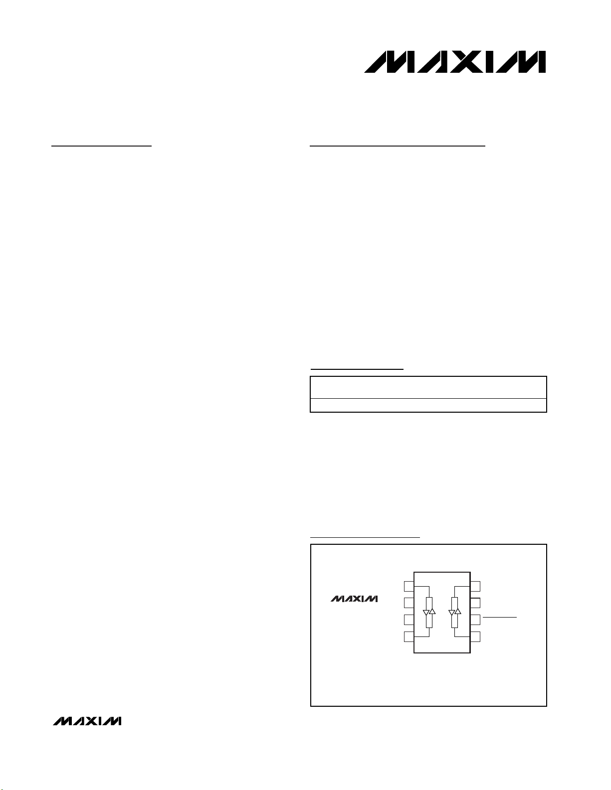
Pin Configurations
19-2328; Rev 3; 9/03
For pricing, delivery, and ordering information, please contact Maxim/Dallas Direct! at
1-888-629-4642, or visit Maxim’s website at www.maxim-ic.com.
Ordering Information
UCSP is a trademark of Maxim Integrated Products, Inc.
SPI is a trademark of Motorola, Inc.
I
2
C is a trademark of Phillips Corp.
MICROWIRE is a trademark of National Semiconductor Corp.
Ordering Information continued at end of data sheet.
Selector Guide appears at end of data sheet.
Pin Configurations continued at end of data sheet.
PART NUMBER TEMP RANGE
MAX3372EEKA-T -40°C to +85°C 8 SOT23-8
PINPACKAGE
MAX3372E/
MAX3373E
I/O VCC2
GND
V
L
1
2
3
4
SOT23-8
TOP VIEW
87I/O VCC1
V
CC
6
THREE-STATE
5
I/O VL1I/O VL2
Page 2
MAX3372E–MAX3379E/MAX3390E–MAX3393E
±15kV ESD-Protected, 1µA, 16Mbps, Dual/Quad
Low-Voltage Level Translators in UCSP
2 _______________________________________________________________________________________
ABSOLUTE MAXIMUM RATINGS
ELECTRICAL CHARACTERISTICS
(VCC= +1.65V to +5.5V, VL= +1.2V to (VCC+ 0.3V), GND = 0, I/O VL_and I/O V
CC_
unconnected, TA= T
MIN
to T
MAX
, unless other-
wise noted. Typical values are at V
CC
= +3.3V, VL= +1.8V, TA= +25°C.) (Notes 1, 2)
Stresses beyond those listed under “Absolute Maximum Ratings” may cause permanent damage to the device. These are stress ratings only, and functional
operation of the device at these or any other conditions beyond those indicated in the operational sections of the specifications is not implied. Exposure to
absolute maximum rating conditions for extended periods may affect device reliability.
All Voltages Referenced to GND
V
CC
...........................................................................-0.3V to +6V
I/O V
CC_
......................................................-0.3V to (VCC+ 0.3V)
I/O V
L_
...........................................................-0.3V to (VL+ 0.3V)
THREE-STATE...............................................-0.3V to (V
L
+ 0.3V)
Short-Circuit Duration I/O V
L
, I/O VCCto GND...........Continuous
Short-Circuit Duration I/O V
L
or I/O VCCto GND
Driven from 40mA Source
(except MAX3372E and MAX3377E) .....................Continuous
Continuous Power Dissipation (T
A
= +70°C)
8-Pin SOT23 (derate 8.9mW/°C above +70°C)...........714mW
3 x 3 UCSP (derate 4.7mW/°C above +70°C) ............379mW
3 x 4 UCSP (derate 6.5mW/°C above +70°C) ............579mW
14-Pin TSSOP (derate 9.1mW/°C above +70°C) ........727mW
Operating Temperature Range ...........................-40°C to +85°C
Storage Temperature Range .............................-65°C to +150°C
Lead Temperature (soldering, 10s) .................................+300°C
POWER SUPPLIES
VL Supply Range V
VCC Supply Range V
Supply Current from V
Supply Current from V
V
Supply Current
V
Supply Current
Three-State Output Mode
Leakage Current
I/O V
THRE E - STATE P in Inp ut Leakag eT
ESD PROTECTION
LOGIC-LEVEL THRESHOLDS (MAX3372E/MAX3377E)
I/O V
I/O VL_ Input Voltage Low V
PARAMETER SYMBOL CONDITIONS MIN TYP MAX UNITS
CC
L
Three-State Output Mode
CC
Three-State Output Mode
L
and I/O V
L_
Input Voltage High V
L_
CC_
L
CC
I
QV
CC
I
QV
L
I
THREE-STATE-VCCTA
I
THREE-STATE-VLTA
I
THREE-STATE-LKGTA
IHL
ILL
= +25°C, THREE-STATE = GND 0.03 1 µA
= +25°C, THREE-STATE = GND 0.03 1 µA
= +25°C, THREE-STATE = GND 0.02 1 µA
= +25°C 0.02 1 µA
A
IEC 1000-4-2 Air-Gap Discharge ±8
IEC 1000-4-2 Contact Discharge ±8I/O VCC (Note 3)
Human Body Model ±15
1.2 5.5 V
1.65 5.50 V
130 300 µA
16 100 µA
VL - 0.2 V
0.15 V
kV
Page 3
MAX3372E–MAX3379E/MAX3390E–MAX3393E
±15kV ESD-Protected, 1µA, 16Mbps, Dual/Quad
Low-Voltage Level Translators in UCSP
_______________________________________________________________________________________ 3
ELECTRICAL CHARACTERISTICS (continued)
(VCC= +1.65V to +5.5V, VL= +1.2V to (VCC+ 0.3V), GND = 0, I/O VL_and I/O V
CC_
unconnected, TA= T
MIN
to T
MAX
, unless other-
wise noted. Typical values are at V
CC
= +3.3V, VL= +1.8V, TA= +25°C.) (Notes 1, 2)
I/O V
I/O V
PARAMETER SYMBOL CONDITIONS MIN TYP MAX UNITS
Input Voltage High V
CC_
Input Voltage Low V
CC_
I/O VL_ Output Voltage High V
I/O VL_ Output Voltage Low V
I/O V
I/O V
Output Voltage High V
CC_
Output Voltage Low V
CC_
THREE-STATE Input Voltage
High
THREE-STATE Input Voltage
Low
IHC
ILC
I/O V
source current = 20µA,
OHL
OLL
OHC
OLC
V
IL-THREE-STATE
V
IL-THREE-STATE
L_
I/O V
I/O V
I/O V
I/O V
I/O V
I/O V
I/O V
> VCC - 0.4V
CC_
sink current = 20µA,
L_
< 0.15V
CC_
source current = 20µA,
CC_
> V
L _
sink current = 20µA,
CC_
< 0.15V
L_
- 0.2V
L
LOGIC-LEVEL THRESHOLDS (MAX3373E–MAX3376E/MAX3378E/MAX3379E and MAX3390E–MAX3393E)
I/O VL_ Input Voltage High V
I/O V
Input Voltage Low V
L_
I/O V
I/O V
Input Voltage High V
CC_
Input Voltage Low V
CC_
I/O VL_ Output Voltage High V
I/O VL_ Output Voltage Low V
I/O V
I/O V
Output Voltage High V
CC_
Output Voltage Low V
CC_
THREE-STATE Input Voltage
High
THREE-STATE Input Voltage
Low
IHL
ILL
IHC
ILC
OHL
OLL
OHC
OLC
V
IH-THREE-STATE
V
IL-THREE-STATE
I/O V
source current = 20µA,
L_
I/O V
I/O V
I/O V
I/O V
I/O V
I/O V
I/O V
≥ VCC - 0.4V
CC_
sink current = 1mA,
L_
≤ 0.15V
CC_
source current = 20µA,
CC_
≥ V
- 0.2V
L_
L
sink current = 1mA,
CC_
≤ 0.15V
L_
VCC - 0.4 V
✕
0.67
V
✕
0.67
V
VL - 0.2 V
VL - 0.2 V
VCC - 0.4 V
✕
0.67
V
✕
0.67
V
VL - 0.2 V
L
CC
L
CC
0.15 V
0.4 V
0.4 V
0.15 V
0.15 V
0.15 V
0.4 V
0.4 V
0.15 V
V
V
V
V
Page 4
MAX3372E–MAX3379E/MAX3390E–MAX3393E
±15kV ESD-Protected, 1µA, 16Mbps, Dual/Quad
Low-Voltage Level Translators in UCSP
4 _______________________________________________________________________________________
TIMING CHARACTERISTICS
(VCC= +1.65V to +5.5V, VL= +1.2V to (VCC+ 0.3V), GND = 0, R
LOAD
= 1MΩ, I/O test signal of Figure 1, TA= T
MIN
to T
MAX
, unless
otherwise noted. Typical values are at V
CC
= +3.3V, VL= +1.8V, TA= +25°C, unless otherwise noted.) (Notes 1, 2)
MAX3372E/MAX3377E (C
I/O VCC_ Rise Time (Note 4) t
I/O VCC_ Fall Time (Note 5) t
I/O VL _ Rise Time (Note 4) t
I/O VL _ Fall Time (Note 5) t
Propagation Delay
Channel-to-Channel Skew t
Maximum Data Rate CL = 25pF 230 kbps
M A X3 3 7 3 E– M A X3 3 7 6 E/M A X3 3 7 8 E/ M A X3 3 7 9 E a n d M A X3 3 9 0 E– M A X3 3 9 3 E ( C
+1.2V ≤ VL ≤ VCC ≤ +5.5V
I/O VCC_ Rise Time (Note 4) t
I/O VCC_ Fall Time (Note 5) t
I/O VL _ Rise Time (Note 4) t
I/O VL _ Fall Time (Note 5) t
Propagation Delay
Channel-to-Channel Skew t
Maximum Data Rate
PARAMETER SYM B O L CONDITIONS MIN TYP MAX UNITS
= 50pF)
LOAD
RVCC
FVCC
RVL
FVL
I/O
I/O
I/O
I/O
VL-VCC
VCC-VL
SKEW
RVCC
FVCC
RVL
LFV
VL-VCC
VCC-VL
SKEW
Driving I/O VL _ 1.6
Driving I/O VCC_ 1.6
Each translator equally loaded 500 ns
Open-drain driving 170 400
Open-drain driving 20 50
Open-drain driving 180 400
Open-drain driving 30 60
Driving I/O VL _
Driving I/O VCC_
Each translator
equally loaded
Open-drain driving 500 kbps
= 15 p F , Dr iv e r O u t p u t Im p e d a n c e ≤ 5 0 Ω)
LOA D
Open-drain driving 210 1000
Open-drain driving 190 1000
Open-drain driving 50
µs
ns
ns
ns
ns
ns
ns
1100 ns
1000 ns
600 ns
1100 ns
725
637
830
330
530
430
20
8 Mbps
Page 5
MAX3372E–MAX3379E/MAX3390E–MAX3393E
±15kV ESD-Protected, 1µA, 16Mbps, Dual/Quad
Low-Voltage Level Translators in UCSP
_______________________________________________________________________________________ 5
Note 1: All units are 100% production tested at TA= +25°C. Limits over the operating temperature range are guaranteed by design
and not production tested.
Note 2: For normal operation, ensure V
L
< (VCC+ 0.3V). During power-up, VL> (VCC+ 0.3V) will not damage the device.
Note 3: To ensure maximum ESD protection, place a 1µF capacitor between V
CC
and GND. See Applications Circuits.
Note 4: 10% to 90%
Note 5: 90% to 10%
TIMING CHARACTERISTICS (continued)
(VCC= +1.65V to +5.5V, VL= +1.2V to (VCC+ 0.3V), GND = 0, R
LOAD
= 1MΩ, I/O test signal of Figure 1, TA= T
MIN
to T
MAX
, unless
otherwise noted. Typical values are at V
CC
= +3.3V, VL= +1.8V, TA= +25°C, unless otherwise noted.) (Notes 1, 2)
+1.2V ≤ VL ≤ VCC ≤ +3.3V
I/O VCC_ Rise Time (Note 4) t
I/O VCC_ Fall Time (Note 5) t
I/O VL _ Rise Time (Note 4) t
I/O VL _ Fall Time (Note 5) t
Propagation Delay
Channel-to-Channel Skew t
Maximum Data Rate
+2.5V ≤ VL ≤ VCC ≤ +3.3V
I/O VCC_ Rise Time (Note 4) t
I/O VCC_ Fall Time (Note 5) t
I/O VL _ Rise Time (Note 4) t
I/O VL _ Fall Time (Note 5) t
Propagation Delay
Channel-to-Channel Skew t
Maximum Data Rate 16 Mbps
+1.8V ≤ VL ≤ VCC ≤ +2.5V
I/O VCC_ Rise Time (Note 4) t
I/O VCC_ Fall Time (Note 5) t
I/O VL _ Rise Time (Note 4) t
I/O VL _ Fall Time (Note 5) t
Propagation Delay
Channel-to-Channel Skew t
Maximum Data Rate 16 Mbps
PARAMETER SYM B O L CONDITIONS MIN TYP MAX UNITS
RVCC
FVCC
RVL
FVL
I/O
I/O
I/O
I/O
I/O
I/O
VL-VCC
VCC-VL
SKEW
RVCC
FVCC
RVL
FVL
VL-VCC
VCC-VL
SKEW
RVCC
FVCC
RVL
FVL
VL-VCC
VCC-VL
SKEW
Driving I/O VL _20
Driving I/O VCC_20
Each translator equally loaded
Driving I/O VL _15
Driving I/O VCC_15
Each translator equally loaded 10 ns
Driving I/O VL _15
Driving I/O VCC_15
Each translator equally loaded 10 ns
25 ns
30 ns
30 ns
30 ns
10 ns
10 Mbps
15 ns
15 ns
15 ns
15 ns
15 ns
15 ns
15 ns
15 ns
ns
ns
ns
Page 6
MAX3372E–MAX3379E/MAX3390E–MAX3393E
±15kV ESD-Protected, 1µA, 16Mbps, Dual/Quad
Low-Voltage Level Translators in UCSP
6 _______________________________________________________________________________________
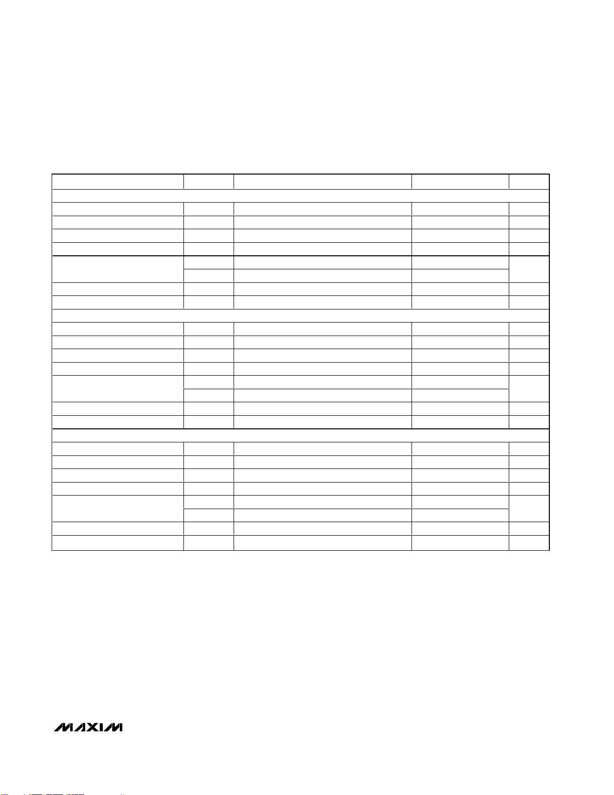
Typical Operating Characteristics
(RL= 1MΩ, TA = +25°C, unless otherwise noted. All 230kbps TOCs apply to MAX3372E/MAX3377E only. All 8Mbps and 500kbps
TOCs apply to MAX3373E–MAX3376E/MAX3378E/MAX3379E and MAX3390E–MAX3393E only.)
VL SUPPLY CURRENT vs. SUPPLY VOLTAGE
(DRIVING I/O V
L
, VCC = +3.3V, VL = +1.8V)
MAX3372E toc01
V
CC
(V)
SUPPLY CURRENT (µA)
4.954.403.853.302.752.20
100
200
300
400
500
600
0
1.65 5.50
8Mbps, C
LOAD
= 15pF
230kbps, C
LOAD
= 50pF
500kbps, OPEN-DRAIN, C
LOAD
= 15pF
VCC SUPPLY CURRENT vs. SUPPLY VOLTAGE
(DRIVING I/O V
L
, VCC = +3.3V, VL = +1.8V)
MAX3372E toc02
V
CC
(V)
SUPPLY CURRENT (mA)
4.954.403.853.302.752.20
0.5
1.0
1.5
2.0
2.5
3.0
3.5
0
1.65 5.50
8Mbps, C
LOAD
= 15pF
230kbps, C
LOAD
= 50pF
500kbps, OPEN-DRAIN, C
LOAD
= 15pF
VL SUPPLY CURRENT vs. TEMPERATURE
(DRIVING I/O V
CC
, VCC = +3.3V, VL = +1.8V)
MAX3372E toc03
TEMPERATURE (°C)
SUPPLY CURRENT (µA)
6035-15 10
50
100
150
200
250
300
350
400
0
-40 85
8Mbps, C
LOAD
= 15pF
230kbps, C
LOAD
= 50pF
500kbps, OPEN-DRAIN, C
LOAD
= 15pF
V
CC
SUPPLY CURRENT vs. TEMPERATURE
(DRIVING I/O V
CC
, VCC = +3.3V, VL = +1.8V)
MAX3372E toc04
TEMPERATURE (°C)
SUPPLY CURRENT (µA)
6035-15 10
200
400
600
800
1000
1200
1400
1600
0
-40 85
8Mbps, C
LOAD
= 15pF
230kbps, C
LOAD
= 50pF
500kbps, OPEN-DRAIN, C
LOAD
= 15pF
VL SUPPLY CURRENT vs. CAPACITIVE LOAD
(DRIVING I/O V
L
, VCC = +3.3V, VL = +1.8V)
MAX3372E toc05
CAPACITIVE LOAD (pF)
SUPPLY CURRENT (µA)
8570554025
50
100
150
200
250
300
350
0
10 100
8Mbps
230kbps
500kbps, OPEN-DRAIN
VCC SUPPLY CURRENT vs. CAPACITIVE LOAD
(DRIVING I/O V
L
, VCC = +3.3V, VL = +1.8V)
MAX3372E toc06
CAPACITIVE LOAD (pF)
SUPPLY CURRENT (µA)
8570554025
500
1000
1500
2000
2500
0
10 100
8Mbps
230kbps
500kbps, OPEN-DRAIN
RISE/FALL TIME vs. CAPACITIVE LOAD
(DRIVING I/O V
L
, V
CC
= +3.3V, VL = +1.8V)
MAX3372E toc07
CAPACITIVE LOAD (pF)
RISE/FALL TIME (ns)
90807060504030
500
1000
1500
2000
2500
0
20 100
DATA RATE = 230kbps
t
HL
t
LH
RISE/FALL TIME vs. CAPACITIVE LOAD
(DRIVING I/O V
L
, VCC = +3.3V, VL = +1.8V)
MAX3372E toc08
CAPACITIVE LOAD (pF)
RISE/FALL TIME (ns)
454030 3520 2515
2
4
6
8
10
12
14
16
18
0
10 50
DATA RATE = 8Mbps
t
HL
t
LH
RISE/FALL TIME vs. CAPACITIVE LOAD
(DRIVING I/O V
L
, VCC = +3.3V, VL = +1.8V)
MAX3372E toc09
CAPACITIVE LOAD (pF)
RISE/FALL TIME (ns)
45403530252015
50
100
150
200
250
0
10 50
t
LH
t
HL
DATA RATE = 500kbps,
OPEN-DRAIN
Page 7
MAX3372E–MAX3379E/MAX3390E–MAX3393E
±15kV ESD-Protected, 1µA, 16Mbps, Dual/Quad
Low-Voltage Level Translators in UCSP
_______________________________________________________________________________________ 7
Typical Operating Characteristics (continued)
(RL= 1MΩ, TA = +25°C, unless otherwise noted. All 230kbps TOCs apply to MAX3372E/MAX3377E only. All 8Mbps and 500kbps
TOCs apply to MAX3373E–MAX3376E/MAX3378E/MAX3379E and MAX3390E–MAX3393E only.)
PROPAGATION DELAY vs. CAPACITIVE LOAD
(DRIVING I/O V
700
600
500
400
300
200
PROPAGATION DELAY (ns)
100
0
20 100
, VCC = +3.3V, VL = +1.8V)
L
t
PHL
t
PLH
DATA RATE = 230kbps
CAPACITIVE LOAD (pF)
RISE/FALL TIME vs. CAPACITIVE LOAD
, V
(DRIVING I/O V
2500
2000
t
1500
1000
RISE/FALL TIME (ns)
500
LH
0
20 100
= +2.5V, VL = +1.8V)
L
CC
DATA RATE = 230kbps
t
HL
CAPACITIVE LOAD (pF)
MAX3372E toc10
90807060504030
MAX3372E toc13
90807060504030
PROPAGATION DELAY vs. CAPACITIVE LOAD
, V
(DRIVING I/O V
15
DATA RATE = 8Mbps
12
9
6
PROPAGATION DELAY (ns)
3
0
10 50
= +3.3V, VL = +1.8V)
L
CC
t
PHL
t
PLH
CAPACITIVE LOAD (pF)
RISE/FALL TIME vs. CAPACITIVE LOAD
(DRIVING I/O V
14
DATA RATE = 8Mbps
12
10
8
6
RISE/FALL TIME (ns)
4
2
0
10 50
, VCC = +2.5V, VL = +1.8V)
L
t
LH
t
HL
CAPACITIVE LOAD (pF)
PROPAGATION DELAY vs. CAPACITIVE LOAD
, V
(DRIVING I/O V
300
t
PLH
250
MAX3372E toc11
200
150
100
PROPAGATION DELAY (ns)
50
45403530252015
t
PHL
0
10 50
= +3.3V, VL = +1.8V)
L
CC
DATA RATE = 500kbps,
OPEN-DRAIN
CAPACITIVE LOAD (pF)
45403530252015
RISE/FALL TIME vs. CAPACITIVE LOAD
, V
(DRIVING I/O V
300
t
LH
250
MAX3372E toc14
200
150
100
RISE/FALL TIME (ns)
t
50
45403530252015
HL
0
10 50
CAPACITIVE LOAD (pF)
= +2.5V, VL = +1.8V)
CC
CC
DATA RATE = 500kbps,
OPEN-DRAIN
45403530252015
MAX3372E toc12
MAX3372E toc15
RISE/FALL TIME vs. CAPACITIVE LOAD
, V
(DRIVING I/O V
2500
DATA RATE = 230kbps
2000
t
1500
1000
RISE/FALL TIME (ns)
500
HL
0
20 100
CAPACITIVE LOAD (pF)
= +3.3V, VL = +1.8V)
CC
CC
t
LH
RISE/FALL TIME vs. CAPACITIVE LOAD
, V
(DRIVING I/O V
12
DATA RATE = 8Mbps
10
MAX3372E toc16
8
t
LH
6
4
RISE/FALL TIME (ns)
2
0
90807060504030
10 50
CAPACITIVE LOAD (pF)
= +3.3V, VL = +1.8V)
CC
CC
t
HL
MAX3372E toc17
45403530252015
RISE/FALL TIME vs. CAPACITIVE LOAD
, V
(DRIVING I/O V
300
250
t
LH
200
150
100
RISE/FALL TIME (ns)
t
50
HL
0
10 50
CAPACITIVE LOAD (pF)
= +3.3V, VL = +1.8V)
CC
CC
DATA RATE = 500kbps,
OPEN-DRAIN
MAX3372E toc18
45403530252015
Page 8
MAX3372E–MAX3379E/MAX3390E–MAX3393E
±15kV ESD-Protected, 1µA, 16Mbps, Dual/Quad
Low-Voltage Level Translators in UCSP
8 _______________________________________________________________________________________
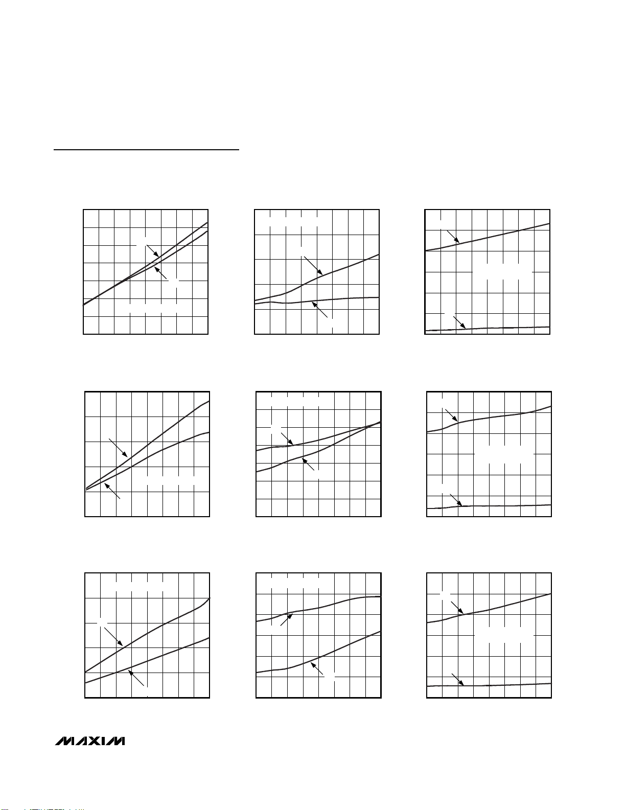
Typical Operating Characteristics (continued)
(RL= 1MΩ, TA = +25°C, unless otherwise noted. All 230kbps TOCs apply to MAX3372E/MAX3377E only. All 8Mbps and 500kbps
TOCs apply to MAX3373E–MAX3376E/MAX3378E/MAX3379E and MAX3390E–MAX3393E only.)
PROPAGATION DELAY vs. CAPACITIVE LOAD
(DRIVING I/O V
CC
, VCC = +3.3V, VL = +1.8V)
MAX3372E toc19
CAPACITIVE LOAD (pF)
PROPAGATION DELAY (ns)
90807060504030
100
200
300
400
500
600
700
0
20 100
DATA RATE = 230kbps
t
PHL
t
PHL
PROPAGATION DELAY vs. CAPACITIVE LOAD
(DRIVING I/O V
CC
, V
CC
= +3.3V, VL = +1.8V)
MAX3372E toc20
CAPACITIVE LOAD (pF)
PROPAGATION DELAY (ns)
45403530252015
1
2
3
4
5
6
0
10 50
DATA RATE = 8Mbps
t
PLH
t
PHL
PROPAGATION DELAY vs. CAPACITIVE LOAD
(DRIVING I/O V
CC
, V
CC
= +3.3V, VL = +1.8V)
MAX3372E toc21
CAPACITIVE LOAD (pF)
PROPAGATION DELAY (ns)
45403530252015
50
100
150
200
250
300
0
10 50
DATA RATE = 500kbps,
OPEN-DRAIN
t
PHL
t
PLH
RISE/FALL TIME vs. CAPACITIVE LOAD
(DRIVING I/O V
CC
, V
CC
= +2.5V, VL = +1.8V)
MAX3372E toc22
CAPACITIVE LOAD (pF)
RISE/FALL TIME (ns)
90807060504030
500
1000
1500
2000
2500
0
20 100
DATA RATE = 230kbps
t
LH
t
HL
RISE/FALL TIME vs. CAPACITIVE LOAD
(DRIVING I/O V
CC
, V
CC
= +2.5V, VL = +1.8V)
MAX3372E toc23
CAPACITIVE LOAD (pF)
RISE/FALL TIME (ns)
403020
2
4
6
8
10
12
0
10 50
t
LH
t
HL
DATA RATE = 8Mbps
RISE/FALL TIME vs. CAPACITIVE LOAD
(DRIVING I/O V
CC
, V
CC
= +2.5V, VL = +1.8V)
MAX3373E toc24
CAPACITIVE LOAD (pF)
RISE/FALl TIME (ns)
403020
50
100
150
200
250
300
350
0
10 50
DATA RATE = 500kbps,
OPEN-DRAIN
t
LH
t
HL
RAIL-TO-RAIL DRIVING
(DRIVING I/O V
L
, VCC = +3.3V, VL = +1.8V,
C
L
= 50pF, DATA RATE = 230kbps)
MAX3372E toc25
I/O V
L_
I/O V
CC_
1V/div
2V/div
1µs/div
RAIL-TO-RAIL DRIVING
(DRIVING I/O V
L
, VCC = +3.3V, VL = +1.8V,
C
L
= 15pF, DATA RATE = 8Mbps)
MAX3372E toc26
I/O V
L_
I/O V
CC_
1V/div
2V/div
200ns/div
Page 9

MAX3372E–MAX3379E/MAX3390E–MAX3393E
±15kV ESD-Protected, 1µA, 16Mbps, Dual/Quad
Low-Voltage Level Translators in UCSP
_______________________________________________________________________________________ 9
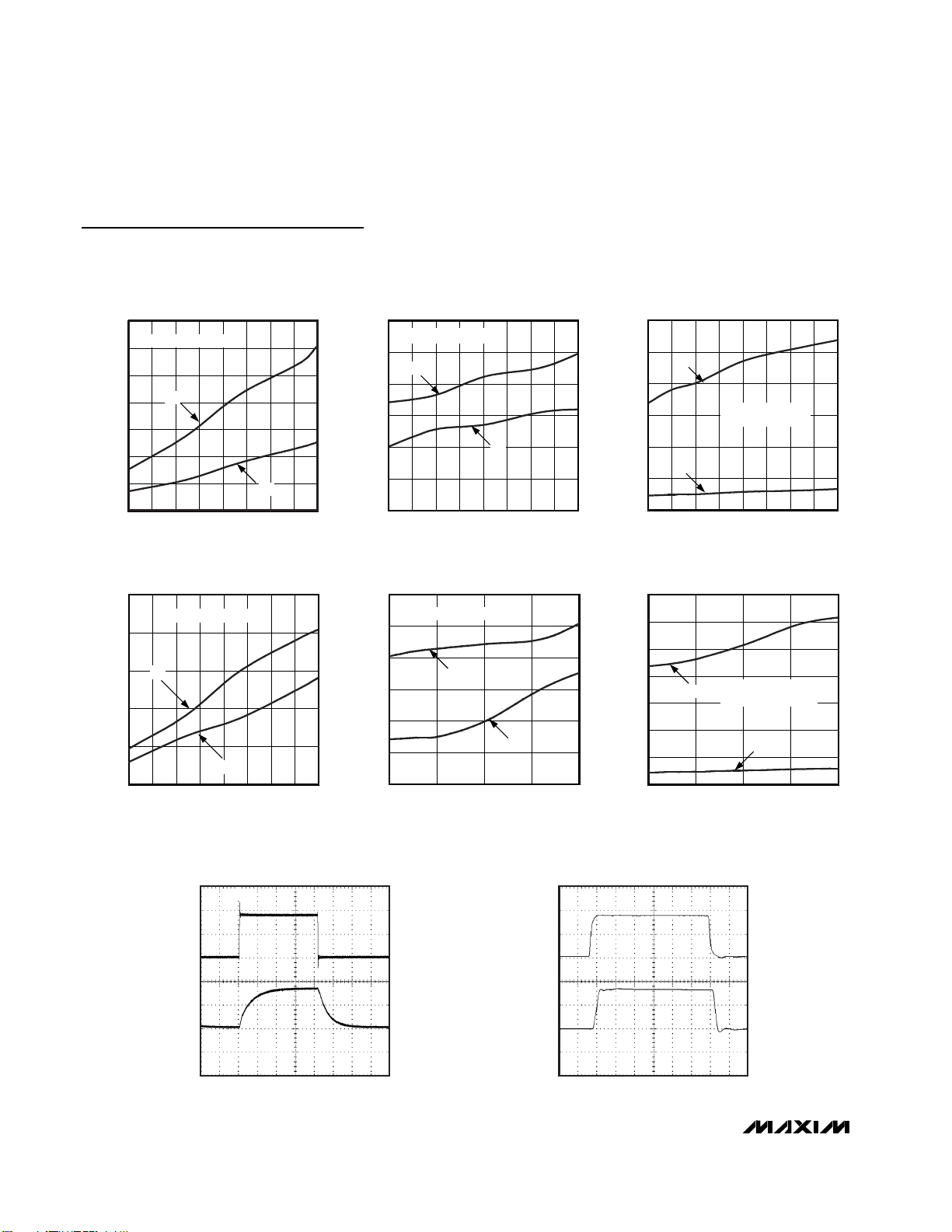
Typical Operating Characteristics (continued)
(RL= 1MΩ, TA = +25°C, unless otherwise noted. All 230kbps TOCs apply to MAX3372E/MAX3377E only. All 8Mbps and 500kbps
TOCs apply to MAX3373E–MAX3376E/MAX3378E/MAX3379E and MAX3390E–MAX3393E only.)
EXITING THREE-STATE OUTPUT MODE
(V
CC
= +3.3V, VL = +1.8V, CL = 50pF)
MAX3372E toc28
I/O V
L_
I/O V
CC_
2µs/div
THREE-STATE
2V/div
1V/div
1V/div
Pin Description
Note 6: For unidirectional devices (MAX3374E/MAX3375E/MAX3376E/MAX3379E and MAX3390E–MAX3393E) see Pin
Configurations for input/output configurations.
OPEN-DRAIN DRIVING
(DRIVING I/O V
L
, VCC = +3.3V, VL = +1.8V,
C
L
= 15pF, DATA RATE = 500kbps)
MAX3372E toc27
I/O V
L_
I/O V
CC_
1V/div
2V/div
200ns/div
3 x 4
UCSP
TSSOP SOT23-8
A1 2 5 C2 I/O VL1 Input/Output 1. Referenced to VL. (Note 6)
A2 3 4 C3 I/O VL2 Input/Output 2. Referenced to VL. (Note 6)
A3 4 — — I/O VL3 Input/Output 3. Referenced to VL. (Note 6)
A4 5 — — I/O VL4 Input/Output 4. Referenced to VL. (Note 6)
B1 14 7 A1 V
B2 1 3 C1 V
B3 8 6 B1
B4 7 2 B3 GND Ground
C1 13 8 A2 I/O VCC1 Input/Output 1. Referenced to VCC. (Note 6)
C2 12 1 A3 I/O VCC2 Input/Output 2. Referenced to VCC. (Note 6)
C3 11 — — I/O VCC3 Input/Output 3. Referenced to VCC. (Note 6)
C4 10 — — I/O VCC4 Input/Output 4. Referenced to VCC. (Note 6)
— 6, 9 — B2 N.C. No Connection. Not internally connected.
PIN
3 x 3
UCSP
NAME FUNCTION
CC
L
VCC Input Voltage +1.65V ≤ VCC ≤ +5.5V.
Logic Input Voltage +1.2V ≤ VL ≤ (VCC + 0.3V)
Thr ee- S tate Outp ut M od e E nab l e. P ul l THREE-STATE l ow
THREE-
STATE
to p l ace d evi ce i n thr ee- state outp ut m od e. I/O V
I/O V L_ ar e hi g h i m p ed ance i n thr ee- state outp ut m od e.
N OTE : Log i c r efer enced to V L ( for l og i c thr eshol d s see
E l ectr i cal C har acter i sti cs) .
C C _
and
Page 10

MAX3372E–MAX3379E/MAX3390E–MAX3393E
±15kV ESD-Protected, 1µA, 16Mbps, Dual/Quad
Low-Voltage Level Translators in UCSP
10 ______________________________________________________________________________________
Detailed Description
The MAX3372E–MAX3379E and MAX3390E–MAX3393E
ESD-protected level translators provide the level shifting
necessary to allow data transfer in a multivoltage system.
Externally applied voltages, VCCand VL, set the logic levels on either side of the device. A low-voltage logic signal
present on the VLside of the device appears as a highvoltage logic signal on the VCCside of the device, and
vice-versa. The MAX3374E/MAX3375E/MAX3376E/
MAX3379E and MAX3390E–MAX3393E unidirectional
level translators level shift data in one direction (VL→
VCCor VCC→ VL) on any single data line. The
MAX3372E/MAX3373E and MAX3377E/MAX3378E bidirectional level translators utilize a transmission-gatebased design (see Figure 2) to allow data translation in
either direction (VL↔ VCC) on any single data line. The
MAX3372E–MAX3379E and MAX3390E–MAX3393E
accept VLfrom +1.2V to +5.5V and VCCfrom +1.65V to
+5.5V, making them ideal for data transfer between lowvoltage ASICs/PLDs and higher voltage systems.
All devices in the MAX3372E–MAX3379E, MAX3390E–
MAX3393E family feature a three-state output mode that
reduces supply current to less than 1µA, thermal shortcircuit protection, and ±15kV ESD protection on the V
CC
side for greater protection in applications that route signals externally. The MAX3372E/MAX3377E operate at a
guaranteed data rate of 230kbps. Slew-rate limiting
reduces EMI emissions in all 230kbps devices. The
MAX3373E–MAX3376E/MAX3378E/MAX3379E and
MAX3390E–MAX3393E operate at a guaranteed data rate
of 8Mbps over the entire specified operating voltage
range. Within specific voltage domains, higher data rates
are possible. (See Timing Characteristics.)
Level Translation
For proper operation ensure that +1.65V ≤ VCC≤ +5.5V,
+1.2V ≤ VL≤ +5.5V, and VL≤ (VCC+ 0.3V). During
power-up sequencing, VL≥ (VCC+ 0.3V) will not damage
the device. During power-supply sequencing, when V
CC
is floating and VLis powering up, a current may be
sourced, yet the device will not latch up. The speed-up
Figure 1a. Rail-to-Rail Driving I/O V
L
Figure 1b. Rail-to-Rail Driving I/O V
CC
Rail-to-Rail is a registered trademark of Nippon Motorola, Ltd.
V
L
MAX3372E–MAX3379E
AND MAX3390E–MAX3393E
I/O VL_
V
V
CC
L
I/O V
V
CC
DATA
_
CC
V
L
MAX3372E–MAX3379E
AND MAX3390E–MAX3393E
DATA
I/O VL_
V
V
CC
L
I/O V
V
CC
_
CC
RISE
,
< 10ns)
R
LOAD
t
PD-VL-LH
GND
t
PD-VL-HL
I/O V
(t
RISE
t
FALL
_
L
,
< 10ns)
t
PD-VCC-LH
GND
R
LOAD
t
PD-VCC-HL
C
LOAD
C
LOAD
I/O VCC_
(t
t
FALL
I/O VCC_
t
RVCC
t
FVCC
I/O VL_
t
RVL
t
FVL
Page 11

MAX3372E–MAX3379E/MAX3390E–MAX3393E
±15kV ESD-Protected, 1µA, 16Mbps, Dual/Quad
Low-Voltage Level Translators in UCSP
______________________________________________________________________________________ 11
circuitry limits the maximum data rate for devices in the
MAX3372E–MAX3379E, MAX3390E–MAX3393E family to
16Mbps. The maximum data rate also depends heavily
on the load capacitance (see Typical Operating
Characteristics), output impedance of the driver, and the
operational voltage range (see Timing Characteristics).
Speed-Up Circuitry
The MAX3373E–MAX3376E/MAX3378E/MAX3379E and
MAX3390E–MAX3393E feature a one-shot generator that
decreases the rise time of the output. When triggered,
MOSFETs PU1 and PU2 turn on for a short time to pull up
I/O VL_and I/O V
CC_
to their respective supplies (see
Figure 2b). This greatly reduces the rise time and propagation delay for the low-to-high transition. The scope
photo of Rail-to-Rail Driving for 8Mbps Operation in the
Typical Operating Characteristics shows the speed-up
circuitry in operation.
Three-State Output Mode
Pull THREE-STATE low to place the MAX3372E–
MAX3379E and MAX3390E–MAX3393E in three-state out-
put mode. Connect THREE-STATE to V
L
(logic high) for
normal operation. Activating the three-state output mode
disconnects the internal 10kΩ pullup resistors on the I/O
VCCand I/O VLlines. This forces the I/O lines to a highimpedance state, and decreases the supply current to
less than 1µA. The high-impedance I/O lines in threestate output mode allow for use in a multidrop network.
When in three-state output mode, do not allow the voltage
at I/O VL_to exceed (VL+ 0.3V), or the voltage at I/O
V
CC_
to exceed (VCC+ 0.3V).
Thermal Short-Circuit Protection
Thermal overload detection protects the MAX3372E–
MAX3379E and MAX3390E–MAX3393E from short-circuit
fault conditions. In the event of a short-circuit fault, when
the junction temperature (TJ) reaches +152°C, a thermal
sensor signals the three-state output mode logic to force
the device into three-state output mode. When TJhas
cooled to +142°C, normal operation resumes.
Figure 1c. Open-Drain Driving I/O V
CC
Figure 1d. Open-Drain Driving I/O V
L
V
L
V
V
CC
L
V
CC
V
L
V
V
CC
L
V
CC
MAX3372E–MAX3379E
AND MAX3390E–MAX3393E
I/O V
L_
GND
I/O V
L_
t
PD-VCC-LH
I/O V
CC_
t
RVCC
I/O V
CC_
t
PD-VCC-HL
DATA
t
FVCC
R
LOAD
MAX3373E–MAX3376E,
MAX3378E/MAX3379E
AND MAX3390E–MAX3393E
DATA
I/O V
C
C
LOAD
LOAD
I/O V
I/O V
CC_
L_
R
LOAD
t
PD-VL-LH
t
RVL
L_
GND
I/O V
CC_
t
PD-VL-HL
t
FVL
Page 12

MAX3372E–MAX3379E/MAX3390E–MAX3393E
±15kV ESD-Protected, 1µA, 16Mbps, Dual/Quad
Low-Voltage Level Translators in UCSP
12 ______________________________________________________________________________________
Figure 2a. Functional Diagram, MAX3372E/MAX3377E (1I/O line)
Figure 2b. Functional Diagram, MAX3373E/MAX3378E (1I/O line)
V
L
P P
I/O V
L
GATE
BIAS
N
V
CC
I/O V
CC
V
CC
I/O V
CC_
I/O V
V
L
PU1 PU2
L_
ONE-SHOT
BLOCK
GATE
BIAS
N
ONE-SHOT
BLOCK
Page 13

MAX3372E–MAX3379E/MAX3390E–MAX3393E
±15kV ESD-Protected, 1µA, 16Mbps, Dual/Quad
Low-Voltage Level Translators in UCSP
______________________________________________________________________________________ 13
±15kV ESD Protection
As with all Maxim devices, ESD-protection structures are
incorporated on all pins to protect against electrostatic
discharges encountered during handling and assembly.
The I/O VCClines have extra protection against static
electricity. Maxim’s engineers have developed state-ofthe-art structures to protect these pins against ESD of
±15kV without damage. The ESD structures withstand
high ESD in all states: normal operation, three-state output mode, and powered down. After an ESD event,
Maxim’s E versions keep working without latchup,
whereas competing products can latch and must be
powered down to remove latchup.
ESD protection can be tested in various ways. The I/O
VCClines of this product family are characterized for
protection to the following limits:
1) ±15kV using the Human Body Model
2) ±8kV using the Contact Discharge method specified
in IEC 1000-4-2
3) ±10kV using IEC 1000-4-2’s Air-Gap Discharge
method
ESD Test Conditions
ESD performance depends on a variety of conditions.
Contact Maxim for a reliability report that documents
test setup, test methodology, and test results.
Human Body Model
Figure 3a shows the Human Body Model and Figure 3b
shows the current waveform it generates when discharged into a low impedance. This model consists of
a 100pF capacitor charged to the ESD voltage of interest, which is then discharged into the test device
through a 1.5kΩ resistor.
IEC 1000-4-2
The IEC 1000-4-2 standard covers ESD testing and
performance of finished equipment; it does not specifically refer to integrated circuits. The MAX3372E–
MAX3379E and MAX3390E–MAX3393E help to design
equipment that meets Level 3 of IEC 1000-4-2, without
the need for additional ESD-protection components.
The major difference between tests done using the
Human Body Model and IEC 1000-4-2 is higher peak current in IEC 1000-4-2, because series resistance is lower
in the IEC 1000-4-2 model. Hence, the ESD withstand
voltage measured to IEC 1000-4-2 is generally lower than
that measured using the Human Body Model. Figure 4a
shows the IEC 1000-4-2 model, and Figure 4b shows the
current waveform for the ±8kV, IEC 1000-4-2, Level 4,
ESD contact-discharge test.
The air-gap test involves approaching the device with a
charged probe. The contact-discharge method connects
the probe to the device before the probe is energized.
Machine Model
The Machine Model for ESD tests all pins using a
200pF storage capacitor and zero discharge resistance. Its objective is to emulate the stress caused by
contact that occurs with handling and assembly during
manufacturing. Of course, all pins require this protection during manufacturing, not just inputs and outputs.
Therefore, after PC board assembly, the Machine
Model is less relevant to I/O ports.
Figure 3a. Human Body ESD Test Model
Figure 3b. Human Body Current Waveform
1MΩ RD 1500Ω
R
C
CHARGE-CURRENT-
LIMIT RESISTOR
HIGH-
VOLTAGE
DC
SOURCE
C
100pF
DISCHARGE
RESISTANCE
STORAGE
s
CAPACITOR
DEVICE
UNDER
TEST
IP 100%
90%
AMPERES
36.8%
10%
0
0
t
RL
I
r
TIME
t
DL
CURRENT WAVEFORM
PEAK-TO-PEAK RINGING
(NOT DRAWN TO SCALE)
Page 14

MAX3372E–MAX3379E/MAX3390E–MAX3393E
±15kV ESD-Protected, 1µA, 16Mbps, Dual/Quad
Low-Voltage Level Translators in UCSP
14 ______________________________________________________________________________________
Applications Information
Power-Supply Decoupling
To reduce ripple and the chance of transmitting incorrect data, bypass VLand VCCto ground with a 0.1µF
capacitor. See Typical Operating Circuit. To ensure full
±15kV ESD protection, bypass VCCto ground with a
1µF capacitor. Place all capacitors as close to the
power-supply inputs as possible.
I2C Level Translation
The MAX3373E–MAX3376E, MAX3378E/MAX3379E
and MAX3390E–MAX3393E level-shift the data present
on the I/O lines between +1.2V and +5.5V, making
them ideal for level translation between a low-voltage
ASIC and an I
2
C device. A typical application involves
interfacing a low-voltage microprocessor to a 3V or 5V
D/A converter, such as the MAX517.
Push-Pull vs. Open-Drain Driving
All devices in the MAX3372E–MAX3379E and
MAX3390E–MAX3393E family may be driven in a pushpull configuration. The MAX3373E–MAX3376E/
MAX3378E/MAX3379E and MAX3390E–MAX3393E
include internal 10kΩ resistors that pull up I/O VL_and
I/O V
CC_
to their respective power supplies, allowing
operation of the I/O lines with open-drain devices. See
Timing Characteristics for maximum data rates when
using open-drain drivers.
Figure 4b. IEC 1000-4-2 ESD Generator Current Waveform
Figure 4a. IEC 1000-4-2 ESD Test Model
MAX3378E–MAX3383E
THREE-STATE
I/O V
L_
DATA
DATA
I/O V
CC_
0.1µF0.1µF
1µF
+3.3V+1.8V
V
CC
+3.3V
SYSTEM
+1.8V
SYSTEM
CONTROLLER
V
L
Typical Operating Circuit
I
100%
50MΩ to 100MΩ RD 330Ω
R
C
90%
DISCHARGE
RESISTANCE
STORAGE
s
CAPACITOR
DEVICE
UNDER
TEST
HIGH-
VOLTAGE
DC
SOURCE
CHARGE-CURRENT-
LIMIT RESISTOR
C
150pF
PEAK
I
10%
tr = 0.7ns to 1ns
30ns
60ns
t
Page 15

MAX3372E–MAX3379E/MAX3390E–MAX3393E
±15kV ESD-Protected, 1µA, 16Mbps, Dual/Quad
Low-Voltage Level Translators in UCSP
______________________________________________________________________________________ 15
Applications Circuits
+1.8V
SYSTEM
CONTROLLER
V
V
L
THREE-STATE
MAX3372E/MAX3373E
I/O V
L1
I/O V
L2
+3.3V+1.8V
0.1µF0.1µF 1µF
CC
+3.3V
SYSTEM
I/O V
I/O V
CC1
CC2
DATADATA
+3.3V+1.8V
0.1µF0.1µF 1µF
V
V
CC
L
+1.8V
SYSTEM
CONTROLLER
THREE-STATE
MAX3374E
I V
L1
I V
L2
O V
O V
CC1
CC2
+3.3V
SYSTEM
DATADATA
Page 16

MAX3372E–MAX3379E/MAX3390E–MAX3393E
±15kV ESD-Protected, 1µA, 16Mbps, Dual/Quad
Low-Voltage Level Translators in UCSP
16 ______________________________________________________________________________________
Applications Circuits (continued)
+3.3V+1.8V
0.1µF0.1µF 1µF
V
V
CC
L
+1.8V
THREE-STATE
SYSTEM
CONTROLLER
MAX3375E
+3.3V
SYSTEM
+1.8V
SYSTEM
CONTROLLER
O V
L1
I V
L2
V
L
THREE-STATE
MAX3376E
I V
CC1
O V
CC2
V
CC
DATADATA
+3.3V+1.8V
0.1µF0.1µF 1µF
+3.3V
SYSTEM
O V
L1
O V
L2
I V
CC1
I V
CC2
DATADATA
Page 17

MAX3372E–MAX3379E/MAX3390E–MAX3393E
±15kV ESD-Protected, 1µA, 16Mbps, Dual/Quad
Low-Voltage Level Translators in UCSP
______________________________________________________________________________________ 17
Applications Circuits (continued)
+1.8V
SYSTEM
CONTROLLER
DATA
V
V
L
THREE-STATE
MAX3377E/MAX3378E
I/O V
L1
I/O V
L2
I/O V
L3
I/O V
L4
0.1µF0.1µF 1µF
CC
+3.3V
SYSTEM
I/O V
CC1
I/O V
I/O V
I/O V
CC2
CC3
CC4
DATA
+3.3V+1.8V
+3.3V+1.8V
0.1µF 1µF
V
V
CC
L
+1.8V
SYSTEM
CONTROLLER
DATA
THREE-STATE
MAX3379E
I V
L1
I V
L2
I V
L3
I V
L4
O V
O V
O V
O V
CC1
CC2
CC3
CC4
DATA
0.1µF
+3.3V
SYSTEM
Page 18

MAX3372E–MAX3379E/MAX3390E–MAX3393E
±15kV ESD-Protected, 1µA, 16Mbps, Dual/Quad
Low-Voltage Level Translators in UCSP
18 ______________________________________________________________________________________
Applications Circuits (continued)
+3.3V+1.8V
0.1µF 1µF
V
V
CC
L
+1.8V
SYSTEM
CONTROLLER
THREE-STATE
MAX3390E
0.1µF
+3.3V
SYSTEM
O V
L1
I V
DATA
0.1µF 1µF
+1.8V
SYSTEM
CONTROLLER
L2
I V
L3
I V
L4
V
L
THREE-STATE
MAX3391E
I V
L1
O V
CC2
O V
CC3
O V
CC4
V
CC
DATA
0.1µF
+3.3V
SYSTEM
+3.3V+1.8V
O V
O V
I V
CC1
I V
CC2
CC3
CC4
DATA
O V
DATA
O V
I V
I V
L1
L2
L3
L4
Page 19

MAX3372E–MAX3379E/MAX3390E–MAX3393E
±15kV ESD-Protected, 1µA, 16Mbps, Dual/Quad
Low-Voltage Level Translators in UCSP
______________________________________________________________________________________ 19
Applications Circuits (continued)
+3.3V+1.8V
0.1µF 1µF
V
V
CC
L
+1.8V
SYSTEM
CONTROLLER
THREE-STATE
MAX3392E
0.1µF
+3.3V
SYSTEM
O V
L1
O V
DATA
0.1µF 1µF
+1.8V
SYSTEM
CONTROLLER
L2
O V
L3
I V
L4
V
THREE-STATE
MAX3393E
L
I V
CC1
I V
CC2
I V
CC3
O V
CC4
V
CC
DATA
0.1µF
+3.3V
SYSTEM
+3.3V+1.8V
I V
CC1
I V
CC2
I V
CC3
I V
CC4
DATA
DATA
O V
O V
O V
I V
L1
L2
L3
L4
Page 20

MAX3372E–MAX3379E/MAX3390E–MAX3393E
±15kV ESD-Protected, 1µA, 16Mbps, Dual/Quad
Low-Voltage Level Translators in UCSP
20 ______________________________________________________________________________________
Selector Guide
PART NUMBER
LEVEL
TRANS-
Tx/
DATA
RATE
TOP
MARK
MAX3372EEKA-T Bi
AAKO
MAX3372EEBL-T Bi
AAR
MAX3373EEKA-T Bi
AAKS
MAX3373EEBL-T Bi
AAZ
MAX3374EEKA-T Uni
AALH
MAX3374EEBL-T Uni
ABA
MAX3375EEKA-T Uni
AALI
MAX3375EEBL-T Uni
ABB
MAX3376EEKA-T Uni
AALG
MAX3376EEBL-T Uni
AAV
MAX3377EEUD Bi
—
MAX3377EEBC-T Bi
AAX
MAX3378EEUD Bi
—
MAX3378EEBC-T Bi
AAY
MAX3379EEUD Uni
—
MAX3379EEBC-T Uni
AAZ
MAX3390EEUD Uni
—
MAX3390EEBC-T Uni
ABA
MAX3391EEUD Uni
—
MAX3391EEBC-T Uni
ABB
MAX3392EEUD Uni
—
MAX3392EEBC-T Uni
ABC
MAX3393EEUD Uni
—
MAX3393EEBC-T Uni
ABD
†
Tx = V
L
→ V
CC
, Rx = V
CC
→ V
L
*Higher data rates are possible (see Timing Characteristics).
Ordering Information (continued)
*Future product—contact factory for availability.
LATION
†
Rx
2/2
230kbps
2/2
2/2
2/2
2/0
2/0
8Mbps*
1/1
1/1
0/2
0/2
4/4
230kbps
4/4
4/4
4/4
4/0
4/0
3/1
3/1
8Mbps*
2/2
2/2
1/3
1/3
0/4
0/4
PART NUMBER TEMP RANGE
MAX3372EEBL-T -40°C to +85°C3
MAX3373EEKA-T -40°C to +85°C 8 SOT23-8
MAX3373EEBL-T -40°C to +85°C3
MAX3374EEKA-T -40°C to +85°C 8 SOT23-8
MAX3374EEBL-T -40°C to +85°C3
MAX3375EEKA-T -40°C to +85°C 8 SOT23-8
MAX3375EEBL-T -40°C to +85°C3
MAX3376EEKA-T -40°C to +85°C 8 SOT23-8
MAX3376EEBL-T -40°C to +85°C3
MAX3377EEUD -40°C to +85°C 14 TSSOP
MAX3377EEBC-T -40°C to +85°C3
MAX3378EEUD -40°C to +85°C 14 TSSOP
MAX3378EEBC-T -40°C to +85°C3
MAX3379EEUD* -40°C to +85°C 14 TSSOP
MAX3379EEBC-T* -40°C to +85°C3
MAX3390EEUD* -40°C to +85°C 14 TSSOP
MAX3390EEBC-T* -40°C to +85°C3
MAX3391EEUD* -40°C to +85°C 14 TSSOP
MAX3391EEBC-T* -40°C to +85°C3
MAX3392EEUD* -40°C to +85°C 14 TSSOP
MAX3392EEBC-T* -40°C to +85°C3
MAX3393EEUD* -40°C to +85°C 14 TSSOP
MAX3393EEBC-T* -40°C to +85°C3
PINPACKAGE
✕
3 UCSP
✕
3 UCSP
✕
3 UCSP
✕
3 UCSP
✕
3 UCSP
✕
4 UCSP
✕
4 UCSP
✕
4 UCSP
✕
4 UCSP
✕
4 UCSP
✕
4 UCSP
✕
4 UCSP
Page 21

MAX3372E–MAX3379E/MAX3390E–MAX3393E
±15kV ESD-Protected, 1µA, 16Mbps, Dual/Quad
Low-Voltage Level Translators in UCSP
______________________________________________________________________________________ 21
Pin Configurations (continued)
1
2
3
1
2
3
A
V
CC
I/O VCC1
I/O V
CC
A
V
CC
O VCC1
O V
CC
A
BC
THREE-STATE
N.C.
GND
2
3 x 3 UCSP
BC
THREE-STATE
N.C.
GND
2
3 x 3 UCSP
BC
V
I/O V
I/O V
I V
I V
GND
1
2
3
V
L
4
I/O VCC2
L
MAX3372E/
MAX3373E
1
L
2
L
87I/O VCC1
V
CC
6
THREE-STATE
5
I/O VL1I/O VL2
SOT23-8
TOP VIEW
1
O VCC2
V
L
1
L
2
L
MAX3374E
GND
2
3
V
L
4
SOT23-8
87O VCC1
V
CC
6
THREE-STATE
5
I VL1I VL2
TOP VIEW
1
1
V
THREE-STATE
CC
2
O VCC1
3
I V
1
V
2
I VCC1
3
I V
2
CC
A
CC
2
CC
N.C.
GND
3 x 3 UCSP
BC
THREE-STATE
N.C.
GND
I V
O V
O V
O V
V
L
1
L
2
L
V
L
1
L
2
L
MAX3375E
MAX3376E
O VCC2
GND
I VCC2
GND
2
3
V
L
4
SOT23-8
TOP VIEW
1
2
3
V
L
4
87I VCC1
V
CC
6
THREE-STATE
5
O VL1I VL2
87I VCC1
V
CC
6
THREE-STATE
5
O VL1O VL2
SOT23-8
3 x 3 UCSP
TOP VIEW
Page 22

MAX3372E–MAX3379E/MAX3390E–MAX3393E
±15kV ESD-Protected, 1µA, 16Mbps, Dual/Quad
Low-Voltage Level Translators in UCSP
22 ______________________________________________________________________________________
Pin Configurations (continued)
A
1
2
3
4
BC
3 x 4 UCSP
V
CC
I/O VCC1
I/O V
CC
2
I/O V
CC
3
I/O V
L
3
I/O V
L
2
I/O V
L
1
V
L
I/O VCC4
GND
I/O V
L
4
THREE-STATE
14
13
12
11
10
9
8
1
2
3
4
5
6
7
V
CC
O VCC1
O V
CC
2
O V
CC
3I VL3
I V
L
2
I V
L
1
V
L
MAX3379E
O VCC4
N.C.
THREE-STATEGND
N.C.
I V
L
4
TSSOP-14
A
1
2
3
4
BC
3 x 4 UCSP
V
CC
O VCC1
O V
CC
2
O V
CC
3
I V
L
3
I V
L
2
I VL1
V
L
O VCC4
GND
I V
L
4
THREE-STATE
14
13
12
11
10
9
8
1
2
3
4
5
6
7
V
CC
I VCC1
O V
CC
2
O V
CC
3I VL3
I V
L
2
O V
L
1
V
L
MAX3390E
O VCC4
N.C.
THREE-STATEGND
N.C.
I V
L
4
TSSOP-14
A
1
2
3
4
BC
3 x 4 UCSP
V
CC
I VCC1
O V
CC
2
O V
CC
3
I V
L
3
I V
L
2
O VL1
V
L
O VCC4
GND
I V
L
4
THREE-STATE
14
13
12
11
10
9
8
1
2
3
4
5
6
7
V
CC
I/0 VCC1
I/0 V
CC
2
I/0 V
CC
3IO VL3
IO V
L
2
IO V
L
1
V
L
MAX3377E/
MAX3378E
I/0 VCC4
N.C.
THREE-STATEGND
N.C.
O V
L
4
TSSOP-14
Page 23

MAX3372E–MAX3379E/MAX3390E–MAX3393E
±15kV ESD-Protected, 1µA, 16Mbps, Dual/Quad
Low-Voltage Level Translators in UCSP
______________________________________________________________________________________ 23
Pin Configurations (continued)
A
1
2
3
4
BC
3 x 4 UCSP
V
CC
I VCC1
I V
CC
2
I V
CC
3
O V
L
3
O V
L
2
O V
L
1
V
L
I VCC4
GND
O V
L
4
THREE-STATE
14
13
12
11
10
9
8
1
2
3
4
5
6
7
V
CC
I VCC1
I V
CC
2
I V
CC
3O VL3
O V
L
2
O V
L
1
V
L
MAX3393E
I VCC4
N.C.
THREE-STATEGND
N.C.
O VL4
TSSOP-14
A
1
2
3
4
BC
3 x 4 UCSP
V
CC
I VCC1
I V
CC
2
I V
CC
3
O V
L
3
O V
L
2
O VL1
V
L
O VCC4
GND
I V
L
4
THREE-STATE
14
13
12
11
10
9
8
1
2
3
4
5
6
7
V
CC
I VCC1
I V
CC
2
I V
CC
3O VL3
O V
L
2
O V
L
1
V
L
MAX3392E
O VCC4
N.C.
THREE-STATEGND
N.C.
I V
L
4
TSSOP-14
14
13
12
11
10
9
8
1
2
3
4
5
6
7
V
CC
I VCC1
I V
CC
2
I V
CC
3I VL3
O V
L
2
O V
L
1
V
L
MAX3391E
I VCC4
N.C.
THREE-STATEGND
N.C.
I V
L
4
TSSOP-14
A
1
2
3
4
BC
3 x 4 UCSP
V
CC
I VCC1
I V
CC
2
O V
CC
3
I V
L
3
O V
L
2
O VL1
V
L
O VCC4
GND
I V
L
4
THREE-STATE
Page 24

MAX3372E–MAX3379E/MAX3390E–MAX3393E
±15kV ESD-Protected, 1µA, 16Mbps, Dual/Quad
Low-Voltage Level Translators in UCSP
24 ______________________________________________________________________________________
Chip Information
TRANSISTOR COUNT: MAX3372E–MAX3376E: 189
MAX3377E–MAX3379E,
MAX3390E–MAX3393E: 295
PROCESS: BiCMOS
Package Information
(The package drawing(s) in this data sheet may not reflect the most current specifications. For the latest package outline information
go to www.maxim-ic.com/packages
.)
C
PIN 1
I.D. DOT
(SEE NOTE 6)
A
SEE DETAIL "A"
b
C
L
L
e1
D
C
L
A2
e
C
E
A1
L
C
SEATING PLANE C
E1
SYMBOL
A
C
L
L2
e
e1
0
L
L2
MIN
0.90
0.00A1
0.90A2
0.28b
0.09
2.80D
1.50E1
0.30
0.25 BSC.
0.65 BSC.
1.95 REF.
0
0
MAX
1.45
0.15
1.30
0.45
0.20
3.00
3.002.60E
1.75
0.60
8
GAUGE PLANE
NOTE:
1. ALL DIMENSIONS ARE IN MILLIMETERS.
2. FOOT LENGTH MEASURED FROM LEAD TIP TO UPPER RADIUS OF
HEEL OF THE LEAD PARALLEL TO SEATING PLANE C.
3. PACKAGE OUTLINE EXCLUSIVE OF MOLD FLASH & METAL BURR.
4. PACKAGE OUTLINE INCLUSIVE OF SOLDER PLATING.
5. COPLANARITY 4 MILS. MAX.
6. PIN 1 I.D. DOT IS 0.3 MM MIN. LOCATED ABOVE PIN 1.
7. SOLDER THICKNESS MEASURED AT FLAT SECTION OF LEAD
BETWEEN 0.08mm AND 0.15mm FROM LEAD TIP.
8. MEETS JEDEC MO178.
PROPRIETARY INFORMATION
TITLE:
DETAIL "A"
PACKAGE OUTLINE, SOT-23, 8L BODY
REV.DOCUMENT CONTROL NO.APPROVAL
21-0078
SOT23, 8L .EPS
1
D
1
Page 25

MAX3372E–MAX3379E/MAX3390E–MAX3393E
±15kV ESD-Protected, 1µA, 16Mbps, Dual/Quad
Low-Voltage Level Translators in UCSP
Maxim cannot assume responsibility for use of any circuitry other than circuitry entirely embodied in a Maxim product. No circuit patent licenses are
implied. Maxim reserves the right to change the circuitry and specifications without notice at any time.
Maxim Integrated Products, 120 San Gabriel Drive, Sunnyvale, CA 94086 408-737-7600 ____________________ 25
© 2003 Maxim Integrated Products Printed USA is a registered trademark of Maxim Integrated Products.
Package Information (continued)
(The package drawing(s) in this data sheet may not reflect the most current specifications. For the latest package outline information
go to www.maxim-ic.com/packages
.)
TSSOP4.40mm.EPS
 Loading...