

For free samples & the latest literature: http://www.maxim-ic.com, or phone 1-800-998-8800.
For small orders, phone 1-800-835-8769.
General Description
The MAX3387E 3V powered EIA/TIA-232 and V.28/V.24
is a communications interface with low power requirements, high data-rate capabilities, and enhanced electrostatic discharge (ESD) protection. The MAX3387E
has three receivers and three transmitters. All RS-232
inputs and outputs are protected to ±15kV using the
IEC 1000-4-2 Air-Gap Discharge method, ±8kV using
the IEC 1000-4-2 Contact Discharge method, and
±15kV using the Human Body Model.
A proprietary low-dropout transmitter output stage
enables true RS-232 performance from a +3.0V to
+5.5V supply with a dual charge pump. The charge
pump requires only four small 0.1µF capacitors for
operation from a +3.3V supply. The MAX3387E is capable of running at data rates up to 250kbps while maintaining RS-232 compliant output levels.
The MAX3387E has a unique VLpin that allows interoperation in mixed-logic voltage systems. Both input and
output logic levels are pin programmable through the
VLpin. The MAX3387E is available in a space-saving
TSSOP package.
Applications
Subnotebook/Palmtop Computers
PDAs and PDA Cradles
Cell Phone Data Cables
Battery-Powered Equipment
Hand-Held Equipment
Peripherals
Features
♦ VLPin for Compatibility with Mixed-Voltage
Systems
♦ ±15kV ESD Protection on Rx Inputs and Tx Outputs
♦ Low 300µA Supply Current
♦ Guaranteed 250kbps Data Rate
♦ 1µA AutoShutdown Plus™ with Receivers Active
♦ Meets EIA/TIA-232 Specifications Down to 3.0V
MAX3387E
3V, ±15kV ESD-Protected, AutoShutdown Plus
RS-232 Transceiver for PDAs and Cell Phones
________________________________________________________________
Maxim Integrated Products
1
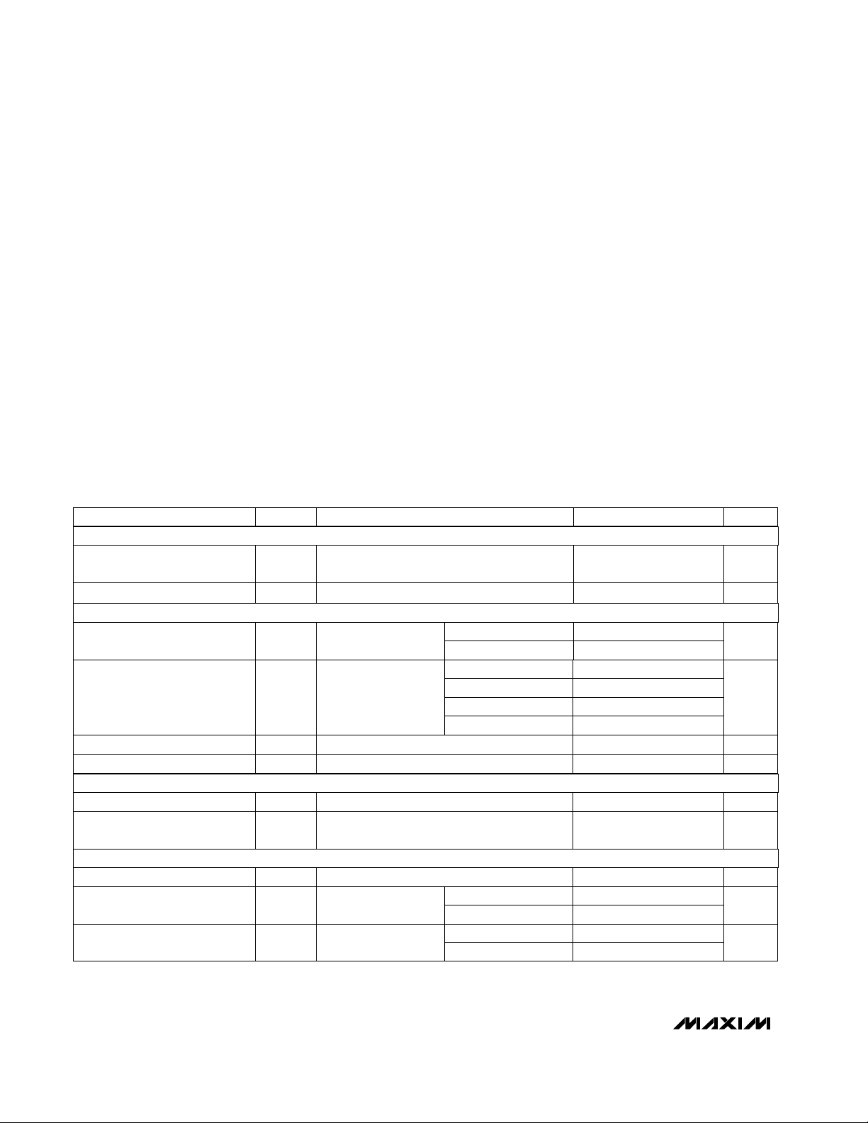
Typical Operating Circuit
19-1561; Rev 1; 10/99
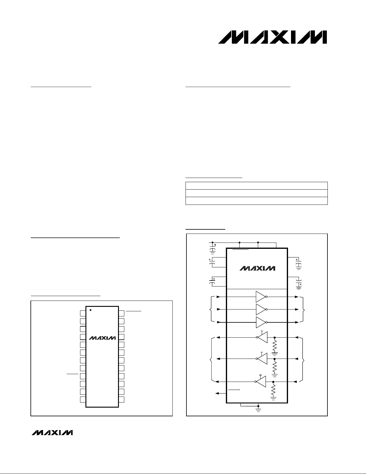
Pin Configuration
Ordering Information
AutoShutdown Plus is a trademark of Maxim Integrated Products.
PART
MAX3387ECUG
MAX3387EEUG
TEMP. RANGE
0°C to +70°C
-40°C to +85°C
PIN-PACKAGE
24 TSSOP
24 TSSOP
TOP VIEW
C1+
C1-
C2-
T1IN
INVALID
T3IN
FORCEON
1
2
V+
3
4
MAX3387E
5
6
V-
7
8
9
10
11
12
TSSOP
24
23
22
21
20
19
18
17
16
15
14
13
FORCEOFF
V
CC
GND
T1OUTC2+
T2OUT
T3OUT
R1IN
R2INT2IN
R3IN
V
L
R1OUT
R2OUTR3OUT
+3.3V
C
BYPASS
C1
0.1µF
C2
0.1µF
TTL/CMOS
INPUTS
TTL/CMOS
OUTPUTS
11
23 15
V
CC
MAX3387E
V
V
V
L
GND
22
L
L
10
9
1
3
4
5
7
8
24
FORCEOFF
C1+
C1-
C2+
C2-
T1IN
T2IN
T3IN
R1OUT14
R2OUT13
R3OUT12
INVALID
FORCEON
V
L
2
V+
6
V-
T1OUT
21
20
T2OUT
19
T3OUT
18
R1IN
5k
R2IN
17
5k
R3IN
16
5k
C3
0.1µF
C4
0.1µF
RS-232
OUTPUTS
RS-232
INPUTS
MAX3387E
3V, ±15kV ESD-Protected, AutoShutdown Plus
RS-232 Transceiver for PDAs and Cell Phones
2 _______________________________________________________________________________________
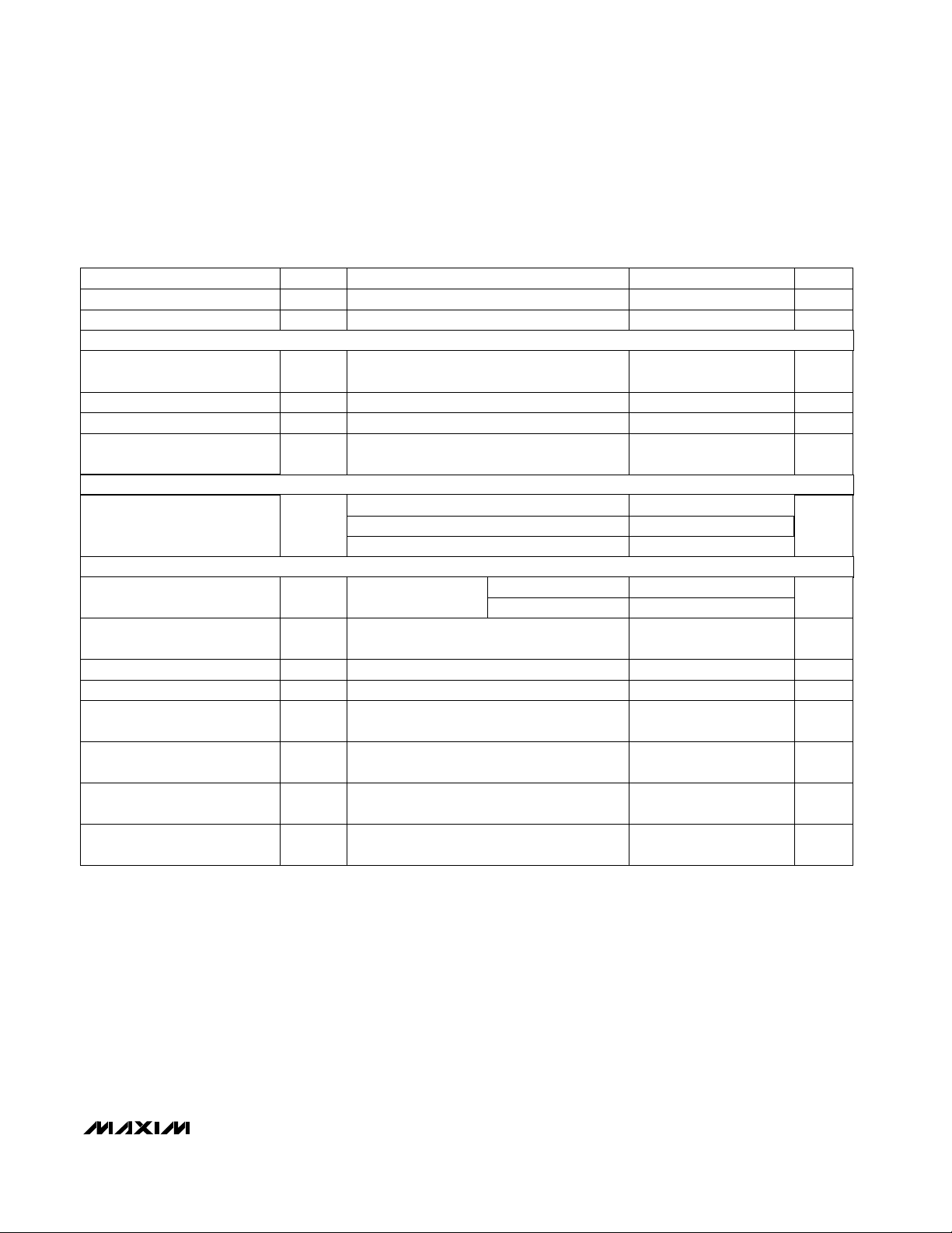
ABSOLUTE MAXIMUM RATINGS
DC ELECTRICAL CHARACTERISTICS
(VCC= VL= +3.0V to +5.5V; C1–C4 = 0.1µF, tested at +3.3V ±10%; C1 = 0.047µF, C2–C4 = 0.33µF, tested at +5.0V ±10%; TA=
T
MIN
to T
MAX
, unless otherwise noted. Typical values are at VCC= VL= +3.3V, TA= +25°C.)
Stresses beyond those listed under “Absolute Maximum Ratings” may cause permanent damage to the device. These are stress ratings only, and functional
operation of the device at these or any other conditions beyond those indicated in the operational sections of the specifications is not implied. Exposure to
absolute maximum rating conditions for extended periods may affect device reliability.
Note 1: V+ and V- can have maximum magnitudes of 7V, but their absolute difference cannot exceed 13V.
V
CC
to GND..............................................................-0.3V to +6V
V
L
to GND...................................................-0.3V to (VCC+ 0.3V)
V+ to GND................................................................-0.3V to +7V
V- to GND .................................................................+0.3V to -7V
V+ + V-(Note 1) .............................................................. +13V
Input Voltages
T_IN, FORCEON, FORCEOFF to GND..................-0.3V to +6V
R_IN to GND .....................................................................±25V
Output Voltages
T_OUT to GND...............................................................±13.2V
R_OUT........................................................-0.3V to (V
L
+ 0.3V)
Short-Circuit Duration T_OUT to GND........................Continuous
Continuous Power Dissipation (T
A
= +70°C)
24-Pin TSSOP (derate 7.8mW/°C above +70°C) ..........625mW
Operating Temperature Ranges
MAX3387ECUG ...................................................0°C to +70°C
MAX3387EEUG ................................................-40°C to +85°C
Junction Temperature......................................................+150°C
Storage Temperature Range .............................-65°C to +150°C
Lead Temperature (soldering, 10sec) .............................+300°C
I
OUT
= 1.6mA
All R_IN idle, FORCEON = GND,
FORCEOFF = V
CC
, all T_IN idle
T_IN, FORCEON, FORCEOFF
T_IN, FORCEON,
FORCEOFF
FORCEOFF = FORCEON = VCC, no load
CONDITIONS
V0.4Output Voltage Low
µA±0.01 ±1Input Leakage Current
V0.5Transmitter Input Hysteresis
V
0.9
Input Logic Threshold High
1.4
2.0
µA1.0 10
Supply Current, AutoShutdown
Plus
2.4
V
0.8
0.3 1 mASupply Current
UNITSMIN TYP MAXSYMBOLPARAMETER
VL= 5.0V
VL= 3.3V
VL= 2.5V
VL= 1.8V
I
OUT
= -1mA V
VL- VL-
0.6 0.1
Output Voltage High
VL= 3.3V or 5.0V
T_IN, FORCEON,
FORCEOFF
0.6
Input Logic Threshold Low
VL= 2.5V
V-25 +25Input Voltage Range
TA= +25°C V
0.8 1.5
Input Threshold Low
VL= 5.0V
VL= 2.5V or 3.3V 0.6 1.2
TA= +25°C V
1.8 2.4
Input Threshold High
VL= 5.0V
VL= 2.5V or 3.3V 1.5 2.4
DC CHARACTERISTICS (VCC= +3.3V or +5V, TA= +25°C)
LOGIC INPUTS
RECEIVER OUTPUTS
RECEIVER INPUTS
MAX3387E
3V, ±15kV ESD-Protected, AutoShutdown Plus
RS-232 Transceiver for PDAs and Cell Phones
_______________________________________________________________________________________ 3
DC ELECTRICAL CHARACTERISTICS (continued)
(VCC= VL= +3.0V to +5.5V; C1–C4 = 0.1µF, tested at +3.3V ±10%; C1 = 0.047µF, C2–C4 = 0.33µF, tested at +5.0V ±10%; TA=
T
MIN
to T
MAX
, unless otherwise noted. Typical values are at VCC= VL= +3.3V, TA= +25°C.)
AutoShutdown Plus (FORCEON = GND, FORCEOFF = V
CC
)
ESD PROTECTION
TRANSMITTER OUTPUTS
-2.7Negative threshold
Figure 3a
Positive threshold
Receiver or Transmitter Edge to
Transmitters Shutdown
t
AUTOSHDN
15 30 60 sec
Receiver Positive or Negative
Threshold to INVALID Low
t
INVL
30
VCC= 5V, Figure 3b
Receiver or Transmitter Edge to
Transmitters Enabled
t
WU
100
µsVCC= 5V, Figure 3b
µsVCC= 5V, Figure 3b
Receiver Positive or Negative
Threshold to INVALID High
t
INVH
1 µs
INVALID Output Voltage Low
0.4
VCC= 5V, Figure 3b
INVALID Output Voltage High
VL- 0.6
VI
OUT
= -1.6mA
VI
OUT
= -1.0mA
Receiver Input Threshold to
INVALID Output Low
-0.3 0.3 V
Receiver Input Threshold to
INVALID Output High
2.7
V
Figure 3a
R_IN, T_OUT
ESD Protection
±8
kV
IEC 1000-4-2 Contact Discharge method
PARAMETER SYMBOL MIN TYP MAX UNITS
Input Hysteresis 0.5 V
Input Resistance 357kΩ
Output Voltage Swing ±5 ±5.4 V
Output Resistance 300 10M Ω
Output Short-Circuit Current ±60 mA
Output Leakage Current ±25 µA
±15
±15
CONDITIONS
TA= +25°C
All transmitter outputs loaded with 3kΩ to
ground
VCC= V+ = V- = 0, transmitter output = ±2V
V
T_OUT
= 0
V
T_OUT
= ±12V, transmitters disabled;
VCC= 0 or 3.0V to 5.5V
Human Body Model
IEC 1000-4-2 Air-Gap Discharge method
TRANSMITTER OUTPUTS
ESD PROTECTION
AutoShutdown Plus (FORCEON = GND, FORCEOFF = V
CC
)
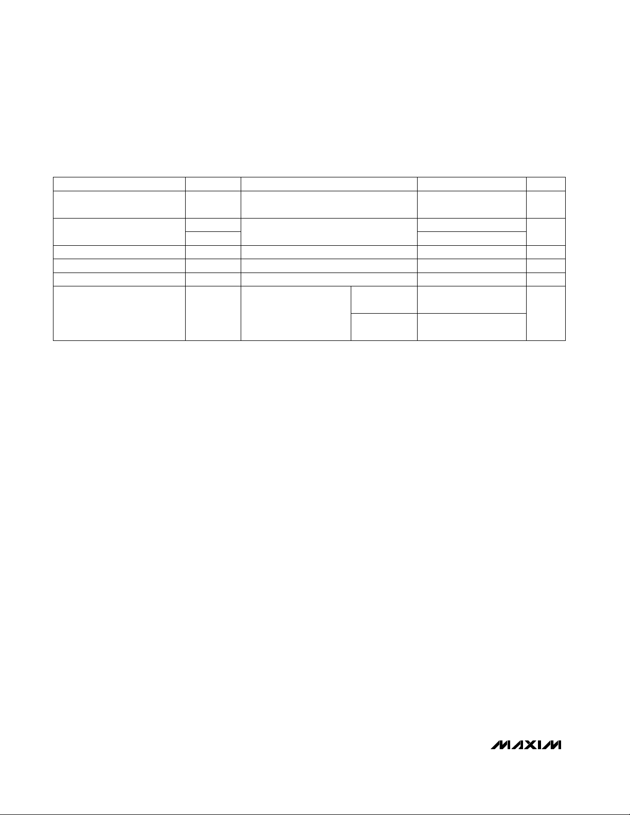
CL= 150pF to
1000pF
CL= 150pF to
2500pF
VCC= 3.3V,
TA= +25°C,
RL= 3kΩ to 7kΩ,
measured from +3V
to -3V or -3V to +3V
RL= 3kΩ, CL= 1000pF,
one transmitter switching
(Note 2)
V/µs
430
V
T_OUT
> 3.7V
Transition-Region Slew
Rate
Receiver input to receiver output,
CL= 150pF
CONDITIONS
630
ns50
t
PHL
- t
PLH
Receiver Skew
ns100
t
PHL
- t
PLH
Transmitter Skew
µs100Time to Exit Shutdown
µs
0.15t
PLH
Receiver Propagation Delay
kbps250Maximum Data Rate
0.15t
PHL
UNITSMIN TYP MAXSYMBOLPARAMETER
TIMING CHARACTERISTICS
(VCC= VL= +3V to +5.5V; C1–C4 = 0.1µF, tested at +3.3V ±10%; C1 = 0.047µF, C2–C4 = 0.33µF, tested at +5.0V ±10%; TA= T
MIN
to T
MAX
, unless otherwise noted. Typical values are at VCC= VL= +3.3V, TA= +25°C.)
MAX3387E
3V, ±15kV ESD-Protected, AutoShutdown Plus
RS-232 Transceiver for PDAs and Cell Phones
4 _______________________________________________________________________________________
MAX3387E
3V, ±15kV ESD-Protected, AutoShutdown Plus
RS-232 Transceiver for PDAs and Cell Phones
_______________________________________________________________________________________
5
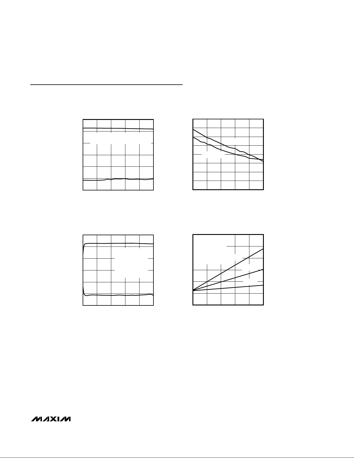
Typical Operating Characteristics
(VCC= VL= +3.3V, TA = +25°C, unless otherwise noted.)
TRANSMITTER OUTPUT VOLTAGE
vs. LOAD CAPACITANCE
7.5
5.0
2.5
-2.5
OUTPUT VOLTAGE (V)
-5.0
-7.5
DATA RATE = 250kbps
LOAD = 3kΩ IN PARALLEL WITH C
0
0 1000 2000 3000 4000 5000
LOAD CAPACITANCE (pF)
L
TRANSMITTER OUTPUT VOLTAGE
vs. DATA RATE
7.5
5.0
2.5
0
-2.5
OUTPUT VOLTAGE (V)
-5.0
LOAD = 3kΩ, 1000pF
ONE TRANSMITTER
SWITCHING AT DATA
RATE, OTHER
TRANSMITTERS
AT 1/8 DATA RATE
MAX3387E-01
MAX3387E-03
SLEW RATE vs. LOAD CAPACITANCE
16
14
12
10
SLEW RATE +
8
6
SLEW RATE (V/µs)
4
2
0
0 1000 2000 3000 4000 5000
LOAD CAPACITANCE (pF)
SUPPLY CURRENT vs. LOAD CAPACITANCE
60
LOAD = 3kΩ,
ONE TRANSMITTER
50
SWITCHING AT DATA
RATE, OTHER
TRANSMITTERS
40
AT 1/8 DATA RATE
30
20
SUPPLY CURRENT (mA)
10
MAX3387E-02
SLEW RATE -
MAX3387E-04
250kbps
120kbps
20kbps
-7.5
0 50 100 150 200 250
DATA RATE (kbps)
0
0 1000 2000 3000 4000 5000
LOAD CAPACITANCE (pF)

MAX3387E
3V, ±15kV ESD-Protected, AutoShutdown Plus
RS-232 Transceiver for PDAs and Cell Phones
6 _______________________________________________________________________________________
C1+ Positive Terminal of the Voltage-Doubler Charge-Pump Capacitor
Pin Descriptions
V+ +5.5V Supply Generated by the Charge Pump
C1- Negative Terminal of the Voltage-Doubler Charge-Pump Capacitor
C2+ Positive Terminal of the Inverting Charge-Pump Capacitor
C2- Negative Terminal of the Inverting Charge-Pump Capacitor
V- -5.5V Generated by the Charge Pump
T1IN
TTL/CMOS Transmitter Inputs
R3OUT
TTL/CMOS Receiver Outputs. Swing between 0 and VL.
R2OUT
R1OUT
V
L
Logic-Level Supply. All CMOS inputs and outputs are referenced to this supply.
R3IN
R2IN
R1IN
RS-232 Receiver Inputs
T3OUT
T2OUT
T1OUT
RS-232 Transmitter Outputs
GND Ground
V
CC
+3.0V to +5.5V Supply Voltage
NAME FUNCTION
FORCEOFF
Force-Off Input. Drive low to shut down transmitters and on-board power supply. This over-
rides all automatic circuitry and FORCEON (Table 1).
1
2
3
4
5
6
7
12
13
14
15
16
17
18
19
20
21
22
23
PIN
24
FORCEON
Force-On Input. Drive high to override automatic circuitry keeping transmitters on
(FORCEOFF must be high) (Table 1).
11
INVALID
Output of the Valid Signal Detector. INVALID is high if a valid RS-232 signal is present on
the receiver inputs.
9
T3IN TTL/CMOS Transmitter Inputs10
8 T2IN

MAX3387E
3V, ±15kV ESD-Protected, AutoShutdown Plus
RS-232 Transceiver for PDAs and Cell Phones
_______________________________________________________________________________________ 7
Detailed Description
Dual Charge-Pump
Voltage Converter
The MAX3387E’s internal power supply consists of a
regulated dual charge pump that provides output voltages of +5.5V (doubling charge pump) and -5.5V
(inverting charge pump), regardless of the input voltage (VCC) over a +3.0V to +5.5V range. The charge
pumps operate in a discontinuous mode: if the output
voltages are less than 5.5V, the charge pumps are
enabled; if the output voltages exceed 5.5V, the charge
pumps are disabled. Each charge pump requires a flying capacitor (C1, C2) and a reservoir capacitor (C3,
C4) to generate the V+ and V- supplies.
RS-232 Transmitters
The transmitters are inverting level translators that convert CMOS-logic levels to 5.0V EIA/TIA-232 levels.
The MAX3387E transmitters guarantee a 250kbps data
rate with worst-case loads of 3kΩ in parallel with
1000pF, providing compatibility with PC-to-PC communication software (such as LapLink™). Transmitters can
be paralleled to drive multiple receivers or mice. Figure 1
shows a complete system connection.
These RS-232 output stages are turned off (high impedance) when the device is in shutdown mode. When the
power is off, the MAX3387E permits the outputs to be
driven up to ±12V.
The transmitter inputs do not have pull-up resistors.
Connect unused inputs to GND or V
L
.
RS-232 Receivers
The receivers convert RS-232 signals to CMOS-logic
output levels. The MAX3387E’s receivers are always
active, even when the device is in shutdown.
The MAX3387E features an INVALID output that indicates when no signal is present on any RS-232 receiver
inputs. INVALID is independent of other control logic
functions; it indicates the receiver input conditions only
(Figures 2 and 3).
Figure 1. Interface Under Control of PMU
LapLink is a trademark of Traveling Software.
Figure 2a. INVALID Function Diagram, INVALID = Low
Figure 2b. INVALID Function Diagram, INVALID = High
POWER-
MANAGEMENT
UNIT OR
KEYBOARD
CONTROLLER
I/O CHIP
POWER SUPPLY
FORCEON
FORCEOFF
INVALID
V
CC
V
L
MAX3387E
+0.3V
R_IN
-0.3V
TRANSMITTERS ARE DISABLED, REDUCING SUPPLY CURRENT TO 1µA IF
ALL RECEIVER INPUTS ARE BETWEEN +0.3V AND -0.3V FOR AT LEAST 30µs.
30µs
COUNTER
R
INVALID
I/O
CHIP
WITH
UART
CPU
RS-232
+2.7V
R_IN
-2.7V
TRANSMITTERS ARE ENABLED IF:
ANY RECEIVER INPUT IS GREATER THAN +2.7V OR LESS THAN -2.7V;
ANY RECEIVER INPUT HAS BEEN BETWEEN +0.3V AND -0.3V FOR LESS THAN 30µs.
30µs
COUNTER
R
INVALID

MAX3387E
3V, ±15kV ESD-Protected, AutoShutdown Plus
RS-232 Transceiver for PDAs and Cell Phones
8 _______________________________________________________________________________________
AutoShutdown Plus Mode
The MAX3387E achieves a1µA supply current with
Maxim’s AutoShutdown Plus feature, which operates
when FORCEOFF is high and a FORCEON is low. When
these devices do not sense a valid signal transition on
any receiver and transmitter input for 30sec, the onboard charge pumps are shut down, reducing supply
current to 1µA. This occurs if the RS-232 cable is disconnected or if the connected peripheral transmitters
are turned off, and if the UART driving the transmitter
inputs is inactive. The system turns on again when a
valid transition is applied to any RS-232 receiver or
transmitter input. As a result, the system saves power
without changes to the existing BIOS or operating system.
Figures 2a and 2b show valid and invalid RS-232
receiver voltage levels. INVALID indicates the receiver
input’s condition, and is independent of FORCEON and
FORCEOFF states. Figure 2 and Table 1 summarize the
MAX3387E’s operating modes. FORCEON and FORCE-
OFF override AutoShutdown Plus circuitry. When neither control is asserted, the IC selects between these
states automatically based on the last receiver or transmitter input edge received.
By connecting FORCEON to INVALID, the MAX3387E
shuts down when no valid receiver level and no receiver or
transmitter edge is detected for 30sec, and wakes up
when a valid receiver level or receiver or transmitter
edge is detected.
By connecting FORCEON and FORCEOFF to INVALID,
the MAX3387E shuts down when no valid receiver level
is detected.
A mouse or other system with AutoShutdown Plus may
need time to wake up. Figure 4 shows a circuit that
forces the transmitters on for 100ms, allowing enough
time for the other system to realize that the MAX3387E
is awake. If the other system outputs valid RS-232 signal transitions within that time, the RS-232 ports on both
systems remain enabled.
VLLogic Supply Input
Unlike other RS-232 interface devices where the receiver outputs swing between 0 and VCC, the MAX3387E
features a separate logic supply input (VL) that sets
VOHfor the receiver outputs and sets thresholds for the
receiver inputs. This feature allows a great deal of flexibility in interfacing to many different types of systems
with different logic levels. Connect this input to the host
logic supply (1.8V ≤ VL≤ VCC). Also, see the
Typical
PDA/Cell-Phone Application
section.
Figure 2c. AutoShutdown Plus Logic
Figure 3a. Receiver Thresholds for INVALID
Figure 2d. Power-Down Logic
EDGE
T_IN
DETECT
EDGE
R_IN
DETECT
FORCEOFF
FORCEON
AUTOSHDN
POWERDOWN IS ONLY AN INTERNAL SIGNAL. IT CONTROLS THE
OPERATIONAL STATUS OF THE TRANSMITTERS AND THE POWER SUPPLIES.
FORCEON
FORCEOFF
S
30sec
TIMER
R
AUTOSHDN
POWERDOWN
TRANSMITTERS ENABLED, INVALID HIGH
+2.7V
INDETERMINATE
+0.3V
-0.3V
RECEIVER INPUT LEVELS
-2.7V
AutoShutdown, TRANSMITTERS DISABLED,
0V
1µA SUPPLY CURRENT, INVALID LOW
INDETERMINATE
TRANSMITTERS ENABLED, INVALID HIGH

MAX3387E
3V, ±15kV ESD-Protected, AutoShutdown Plus
RS-232 Transceiver for PDAs and Cell Phones
_______________________________________________________________________________________ 9
Figure 3b. AutoShutdown Plus/INVALID Timing Diagram
Software-Controlled Shutdown
If direct software control is desired, INVALID can be
used to indicate a DTR or ring indicator signal. Connect
FORCEOFF and FORCEON together to bypass
AutoShutdown so the line acts like a SHDN input.
±15kV ESD Protection
As with all Maxim devices, ESD-protection structures
are incorporated on all pins to protect against electrostatic discharges (ESDs) encountered during handling
and assembly. The MAX3387E driver outputs and
receiver inputs have extra protection against static
electricity. Maxim has developed state-of-the-art structures to protect these pins against ESD of ±15kV without damage. The ESD structures withstand high ESD in
all states: normal operation, shutdown, and powered
down. After an ESD event, Maxim’s “E” version devices
keep working without latchup, whereas competing RS232 products can latch and must be powered down to
remove latchup. ESD protection can be tested in various ways. The transmitter outputs and receiver inputs
of this product family are characterized for protection to
the following limits:
1) ±15kV using the Human Body Model
2) ±8kV using the Contact-Discharge method specified
in IEC 1000-4-2
3) ±15kV using IEC 1000-4-2’s Air-Gap method
Figure 4. AutoShutdown with Initial Turn-On to Wake Up a
System
RECEIVER
INPUTS
TRANSMITTER
INPUTS
TRANSMITTER
OUTPUTS
INVALID
OUTPUT
INVALID
}
REGION
V
CC
t
INVL
0
V+
V
CC
0
V-
t
INVH
t
AUTOSHDN
t
t
WU
AUTOSHDN
t
WU
POWER-
MANAGEMENT
UNIT
MASTER SHDN LINE
FORCEOFF
0.1µF 1M
FORCEON
MAX3387E

MAX3387E
3V, ±15kV ESD-Protected, AutoShutdown Plus
RS-232 Transceiver for PDAs and Cell Phones
10 ______________________________________________________________________________________
ESD Test Conditions
ESD performance depends on a variety of conditions.
Contact Maxim for a reliability report that documents
test setup, methodology, and results.
Human Body Model
Figure 5a shows the Human Body Model, and Figure
5b shows the current waveform it generates when discharged into a low impedance. This model consists of a
100pF capacitor charged to the ESD voltage of interest,
which is then discharged into the test device through a
1.5kΩ resistor.
Table 1. Output Control Truth Table
OPERATION STATUS FORCEON
FORCEOFF
VALID
RECEIVER
LEVEL
RECEIVER OR
TRANSMITTER
EDGE WITHIN
30sec
T_OUT R_OUT
Shutdown
(Forced Off)
X 0 X X High-Z Active
Normal Operation
(Forced On)
1 1 X X Active Active
Normal Operation
(AutoShutdown Plus)
0 1 X Yes Active Active
Shutdown
(AutoShutdown Plus)
0 1 X No High-Z Active
Normal Operation
INVALID
1 Yes X Active Active
Normal Operation
INVALID
1 X Yes Active Active
Shutdown
INVALID
1 No No High-Z Active
Normal Operation
(AutoShutdown)
INVALID INVALID
Yes X Active Active
Shutdown
(AutoShutdown)
INVALID INVALID
No X High-Z Active
Figure 5a. Human Body ESD Test Model
Figure 5b. Human Body Current Waveform
X = Don’t care
R
C
1M
CHARGE-CURRENT
LIMIT RESISTOR
HIGH-
VOLTAGE
DC
SOURCE
100pF
C
s
R
D
1500Ω
DISCHARGE
RESISTANCE
STORAGE
CAPACITOR
DEVICE
UNDER
TEST
PEAK-TO-PEAK RINGING
I
r
(NOT DRAWN TO SCALE)
AMPERES
IP 100%
90%
36.8%
10%
0
0
t
RL
TIME
t
DL
CURRENT WAVEFORM

MAX3387E
3V, ±15kV ESD-Protected, AutoShutdown Plus
RS-232 Transceiver for PDAs and Cell Phones
______________________________________________________________________________________ 11
IEC 1000-4-2
The IEC 1000-4-2 standard covers ESD testing and
performance of finished equipment; it does not specifically refer to ICs. The MAX3387E helps you design
equipment that meets Level 4 (the highest level) of IEC
1000-4-2, without the need for additional ESD-protection components.
The major difference between tests done using the
Human Body Model and IEC 1000-4-2 is higher peak
current in IEC 1000-4-2 because series resistance is
lower in the IEC 1000-4-2 model. Hence, the ESD withstand voltage measured to IEC 1000-4-2 is generally
lower than that measured using the Human Body
Model. Figure 6a shows the IEC 1000-4-2 model, and
Figure 6b shows the current waveform for the ±8kV IEC
1000-4-2 Level 4 ESD Contact Discharge test.
The air-gap test involves approaching the device with a
charged probe. The contact-discharge method connects
the probe to the device before the probe is energized.
Machine Model
The Machine Model for ESD tests all pins using a
200pF storage capacitor and zero discharge resistance. Its objective is to emulate the stress caused by
contact that occurs with handling and assembly during
manufacturing. All pins require this protection during
manufacturing, not just RS-232 inputs and outputs.
Therefore, after PC board assembly, the Machine
Model is less relevant to I/O ports.
__________Applications Information
Capacitor Selection
The capacitor type used for C1–C4 is not critical for
proper operation; polarized or nonpolarized capacitors
can be used. The charge pump requires 0.1µF capaci-
tors for 3.3V operation. For other supply voltages, see
Table 2 for required capacitor values. Do not use values smaller than those listed in Table 2. Increasing the
capacitor values (e.g., by a factor of 2) reduces ripple
on the transmitter outputs and slightly reduces power
consumption. C2, C3, and C4 can be increased without
changing C1’s value. However, do not increase C1
without also increasing the values of C2, C3, and C4 to
maintain the proper ratios (C1 to the other capacitors).
When using the minimum required capacitor values,
make sure the capacitor value does not degrade
excessively with temperature. If in doubt, use capacitors with a larger nominal value. The capacitor’s equivalent series resistance (ESR), which usually rises at low
temperatures, influences the amount of ripple on V+
and V-.
Figure 6a. IEC 1000-4-2 ESD Test Model
Figure 6b. IEC 1000-4-2 ESD Generator Current Waveform
Table 2. Minimum Required Capacitor
Values
V
CC
(V)
0.10.1
C2, C3, C4
(µF)
3.0 to 3.6
0.330.047
10.223.0 to 5.5
4.5 to 5.5
C1
(µF)
R
C
50M to 100M
CHARGE-CURRENT
LIMIT RESISTOR
HIGH-
VOLTAGE
DC
SOURCE
150pF
C
s
RD
330Ω
DISCHARGE
RESISTANCE
STORAGE
CAPACITOR
DEVICE
UNDER
TEST
I
100%
90%
PEAK
I
10%
tR = 0.7ns to 1ns
30ns
60ns
t

MAX3387E
Power-Supply Decoupling
In most circumstances, a 0.1µF bypass capacitor is adequate. In applications that are sensitive to power-supply
noise, decouple VCCto ground with a capacitor of the
same value as charge-pump capacitor C1. Connect
bypass capacitors as close to the IC as possible.
Operation Down to 2.7V
Transmitter outputs will meet EIA/TIA-562 levels of
±3.7V with supply voltages as low as +2.7V.
Transmitter Outputs when
Exiting Shutdown
Figure 7 shows two transmitter outputs when exiting
shutdown mode. As they become active, the two transmitter outputs are shown going to opposite RS-232 levels (one transmitter input is high; the other is low). Each
transmitter is loaded with 3kΩ in parallel with 2500pF.
The transmitter outputs display no ringing or undesirable transients as they come out of shutdown. Note that
the transmitters are enabled only when the magnitude
of V- exceeds approximately 3V.
High Data Rates
The MAX3387E maintains the RS-232 ±5.0V minimum
transmitter output voltage even at high data rates.
Figure 8 shows a transmitter loopback test circuit.
Figure 9 shows a loopback test result at 120kbps, and
Figure 10 shows the same test at 250kbps. For Figure
9, all transmitters were driven simultaneously at
120kbps into RS-232 loads in parallel with 1000pF. For
Figure 10, a single transmitter was driven at 250kbps,
and all transmitters were loaded with an RS-232 receiver in parallel with 1000pF.
Interconnection with
3V and 5V Logic
The MAX3387E can directly interface with various 5V
logic families, including ACT and HCT CMOS. The logic
voltage power-supply pin (VL) sets the output voltage
level of the receivers and the input thresholds of the
transmitters.
3V, ±15kV ESD-Protected, AutoShutdown Plus
RS-232 Transceiver for PDAs and Cell Phones
12 ______________________________________________________________________________________
Figure 8. Loopback Test Circuit
Figure 9. Loopback Test Results at 120kbps
Figure 7. Transmitter Outputs when Exiting Shutdown
5V/div
2V/div
VCC = 3.3V
C1–C4 = 0.1µF
50µs/div
V
CC
0.1µF
V
CC
MAX3387E
V+
C3
V-
C4
C1
C2
C1+
C1-
C2+
C2-
T2
T1
T_ IN
R_ OUT
FORCEOFF
V
CC
FORCEON
GND
T_ OUT
R_ IN
5k
1000pF
T1IN
T1OUT
R1OUT
VCC = 3.3V
2µs/div
5V/div
5V/div
5V/div

MAX3387E
3V, ±15kV ESD-Protected, AutoShutdown Plus
RS-232 Transceiver for PDAs and Cell Phones
______________________________________________________________________________________ 13
Typical PDA/Cell-Phone Application
The MAX3387E is designed with PDA applications in
mind. Two transmitters and two receivers handle standard full-duplex communication protocol, while an extra
transmitter allows a ring indicator signal to alert the
UART on the PC. Without the ring indicator transmitter,
solutions for these applications would require softwareintensive polling of the cradle inputs.
The ring indicate (RI) signal is generated when a PDA,
phone, or other “cradled” device is plugged into its cradle.
This generates a logic-low signal to the RI transmitter
input, creating +6V at the ring indicate pin. The PC’s
UART RI input is the only pin that can generate an interrupt from signals arriving through the RS-232 port. The
interrupt routine for this UART will then service the RS232 full-duplex communication between the PDA and
the PC.
As cell phone design becomes more like that of PDAs,
cell phones will require similar docking ability and communication protocol. Cell phones operate on a single
lithium-ion (Li+) battery and work with a power-supply
voltage of +2.7V to +4V. The baseband logic coming
from the phone connector can be as low as 1.8V at the
transceivers. To prevent forward biasing of a device
internal to the cell phone, the MAX3387E comes with a
logic power-supply pin (V
L
) that limits the logic levels
presented to the phone. The receiver outputs will sink
to zero for low outputs, but will not exceed VLfor logic
highs. The input logic levels for the transmitters are also
altered, scaled by the magnitude of the VLinput. The
device will work with VLas low as 1.8V before the
charge-pump noise will begin to cause the transmitter
outputs to oscillate. This is useful with cell phones and
other power-efficient devices with core logic voltage
levels that go as low as 1.8V.
Figure 10. Loopback Test Results at 250kbps
Chip Information
TRANSISTOR COUNT: 1267
T1IN
T1OUT
R1OUT
VCC = 3.3V
2µs/div
5V/div
5V/div
5V/div

MAX3387E
3V, ±15kV ESD-Protected, AutoShutdown Plus
RS-232 Transceiver for PDAs and Cell Phones
14 ______________________________________________________________________________________
Package Information
TSSOP.EPS

MAX3387E
3V, ±15kV ESD-Protected, AutoShutdown Plus
RS-232 Transceiver for PDAs and Cell Phones
______________________________________________________________________________________ 15
NOTES

MAX3387E
3V, ±15kV ESD-Protected, AutoShutdown Plus
RS-232 Transceiver for PDAs and Cell Phones
Maxim cannot assume responsibility for use of any circuitry other than circuitry entirely embodied in a Maxim product. No circuit patent licenses are
implied. Maxim reserves the right to change the circuitry and specifications without notice at any time.
16
____________________Maxim Integrated Products, 120 San Gabriel Drive, Sunnyvale, CA 94086 408-737-7600
© 1999 Maxim Integrated Products Printed USA is a registered trademark of Maxim Integrated Products.
NOTES
 Loading...