

Page 1
现货库存、技术资料、百科信息、热点资讯,精彩尽在鼎好!
General Description
The MAX3380E/MAX3381E are +2.35V to +5.5V-powered EIA/TIA-232 and V.28/V.24 communication interfaces with low power requirements, high data-rate
capabilities, and enhanced electrostatic discharge
(ESD) protection on both the TTL and RS-232 sides.
The MAX3380E/MAX3381E have two receivers and two
transmitters. All RS-232 inputs, outputs, and logic input
pins are protected to ±15kV using IEC 1000-4-2 AirGap Discharge method and the Human Body Model,
and ±8kV using IEC 1000-4-2 Contact Discharge
method.
The proprietary low-dropout transmitter output stage
enables true RS-232 performance from a +3.1V to
+5.5V supply with a dual charge pump. The parts
reduce the transmitter output levels to RS-232-compatible levels with no increase in supply current for supplies less than +3.1V and greater than +2.35V. The
+2.35V to +5.5V operating range is fully compatible
with lithium-ion (Li+) batteries. The charge pump
requires only four small 0.1µF capacitors for operation.
The MAX3380E/MAX3381E transceivers use Maxim’s
revolutionary AutoShutdown Plus™ feature to automatically enter a 1µA shutdown mode. These
devices shut down the on-board power supply and
drivers when they do not sense a valid signal transition for 30 seconds on either the receiver or transmitter inputs.
The MAX3380E is capable of transmitting data at
rates of 460kbps while maintaining RS-232 output
levels, and the MAX3381E operates at data rates up
to 250kbps. The MAX3381E offers a slower slew rate
for applications where noise and EMI are issues. The
MAX3380E/MAX3381E have a unique V
L
pin that
allows interoperation in mixed-logic voltage systems
down to +1.65V. Both input and output logic levels
are referenced to the V
L
pin. The MAX3380E/MAX3381E
are available in a space-saving TSSOP package.
Applications
Cell Phone Data Lump Cables
PDA Data Lump Cables
GPS Receivers
Digital Cameras
Features
♦ ±15kV ESD Protection on All CMOS and RS-232
Inputs and Outputs (Except INVALID)
±15kV Human Body Model
±15kV IEC 1000-4-2 Air-Gap Discharge
±8kV IEC 1000-4-2 Contact Discharge
♦ Operates Over Entire Li+ Battery Range
♦ Low Logic Threshold Down to +1.65V for
Compatibility with Cell Phone Logic Supply Voltages
♦ 1µA Low-Power AutoShutdown Plus Mode
♦ Compatible with Next-Generation GSM Data Rates
♦ 20-Pin TSSOP Package
MAX3380E/MAX3381E
+2.35V to +5.5V, 1µA, 2Tx/2Rx RS-232 Transceivers
with ±15kV ESD-Protected I/O and Logic Pins
________________________________________________________________ Maxim Integrated Products 1
19-2128; Rev 0; 8/01
Ordering Information
Pin Configuration appears at end of data sheet.
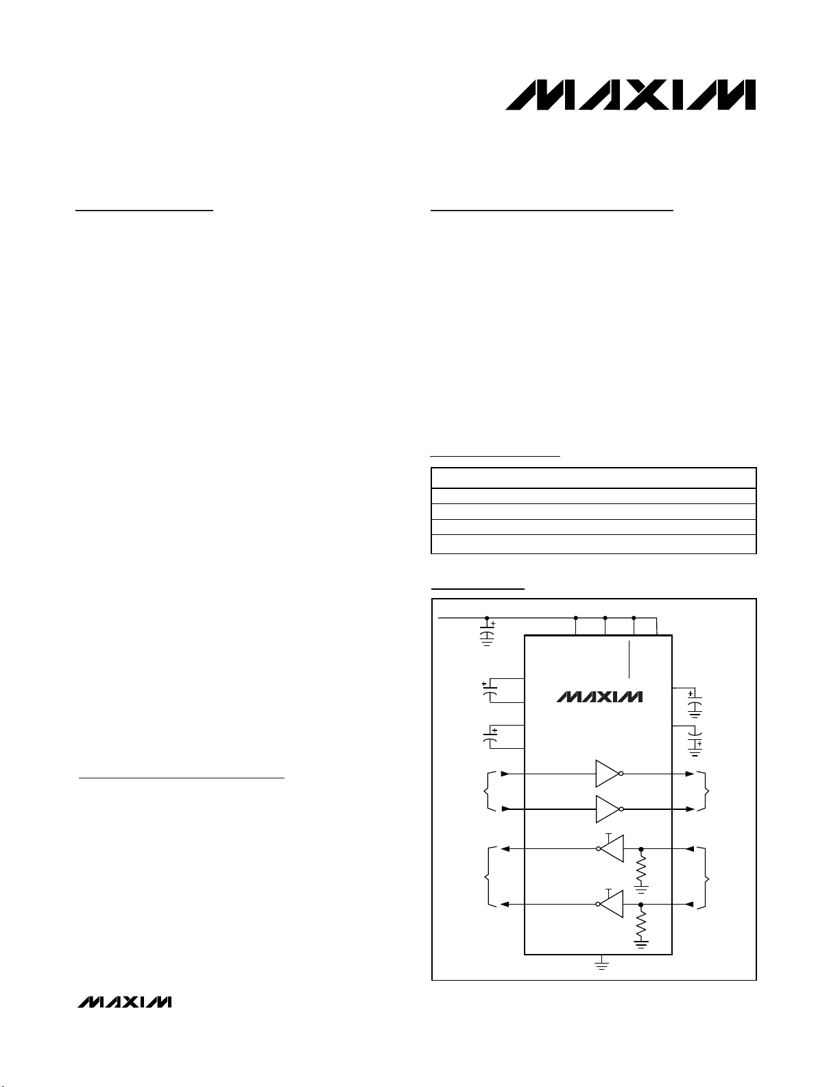
MAX3380E/
MAX3381E
R2OUT
R1OUT
R2IN
GND
RS-232
OUTPUTS
TTL/CMOS
INPUTS
T2IN
T1IN
C2-
C2+
C1-
C1+
R1IN
T2OUT
T1OUT
V-
V+
V
CCVL
C1
0.1µF
C2
0.1µF
C5
0.1µF
+3.3V
RS-232
INPUTS
TTL/CMOS
OUTPUTS
5kΩ
5kΩ
C3
0.1µF
C4
0.1µF
V
L
V
L
FORCEON
FORCEOFF
Typical Operating Circuit
For pricing, delivery, and ordering information, please contact Maxim/Dallas Direct! at
1-888-629-4642, or visit Maxim’s website at www.maxim-ic.com.
AutoShutdown Plus is a trademark of Maxim Integrated Products
PART TEMP. RANGE PIN-PACKAGE
MAX3380ECUP 0°C to +70°C 20 TSSOP
MAX3380EEUP -40°C to +85°C 20 TSSOP
MAX3381ECUP 0°C to +70°C 20 TSSOP
MAX3381EEUP -40°C to +85°C 20 TSSOP
Page 2
MAX3380E/MAX3381E
+2.35V to +5.5V, 1µA, 2Tx/2Rx RS-232 Transceivers
with ±15kV ESD-Protected I/O and Logic Pins
2 _______________________________________________________________________________________
ABSOLUTE MAXIMUM RATINGS
ELECTRICAL CHARACTERISTICS
(VCC= +2.35V to +5.5V, VL= +1.65V to +5.5V. When VCC< +4.5V, C1 = C2 = C3 = C4 = 0.1µF; when VCC≥ +4.5V, C1 = 0.047µF,
C2 = C3 = C4 = 0.33µF; T
A
= T
MIN
to T
MAX
, unless otherwise noted. Typical values are at VCC= VL= +3.3V, TA= +25°C.)
Stresses beyond those listed under “Absolute Maximum Ratings” may cause permanent damage to the device. These are stress ratings only, and functional
operation of the device at these or any other conditions beyond those indicated in the operational sections of the specifications is not implied. Exposure to
absolute maximum rating conditions for extended periods may affect device reliability.
Note 1: V+ and V- can have maximum magnitudes of +7V, but their absolute difference cannot exceed +13V.
V
CC
to GND...........................................................-0.3V to +6.0V
V
L
to GND..............................................................-0.3V to +6.0V
V+ to GND .............................................................-0.3V to +7.0V
V- to GND ..............................................................+0.3V to -7.0V
V+ + |V-| (Note 1) .................................................................+13V
Input Voltages
T_IN, FORCEON, FORCEOFF to GND...............-0.3V to +6.0V
R_IN to GND .....................................................................±25V
Output Voltages
T_OUT to GND...............................................................±13.2V
R_OUT, INVALID to GND...........................-0.3V to (V
L
+ 0.3V)
Short-Circuit Duration T_OUT to GND........................Continuous
Continuous Power Dissipation (T
A
= +70°C)
20-Pin TSSOP (derate 10.9mW/°C over +70°C) .........879mW
Operating Temperature Ranges
MAX3380ECUP/MAX3381ECUP........................0°C to +70°C
MAX3380EEUP/MAX3381EEUP .....................-40°C to +85°C
Junction Temperature......................................................+150°C
Storage Temperature Range .............................-65°C to +150°C
Lead Temperature (soldering, 10s) .................................+300°C
PARAMETER SYMBOL CONDITIONS MIN TYP MAX UNITS
Supply Current, AutoShutdown
Plus
Receivers idle, VT_IN = VCC or GND,
I
CC
FORCEON = GND, FORCEOFF = V
FORCEOFF = GND 1 10
CC
10
µA
Supply Current, Normal Operation I
LOGIC INPUTS (T_IN, FORCEON, FORCEOFF)
Input Logic Threshold Low V
Input Logic Threshold High V
Transmitter Input Hysteresis 0.5 V
Input Leakage Current ±0.01 ±1µA
RECEIVER OUTPUTS (R_OUT) AND INVALID
Output Voltage Low I
Output Voltage High I
RECEIVER INPUTS (R_IN)
Input Voltage Range -25 +25 V
Input Threshold Low TA = +25°C
Input Threshold High TA = +25°C
Input Hysteresis 0.3 V
Input Resistance TA = +25°C 357kΩ
CC
FORCEON = FORCEOFF = VL, no load 0.3 1 mA
VCC = +5.5V, VL = +5.5V 0.4 1.2
IL
VCC = +2.5V, VL = +1.65V 0.4
VCC = +5.5V, VL = +5.5V VL ✕ 0.66
IH
VCC = +2.5V, VL = +1.65V VL ✕ 0.66
= 500µA 0.5 V
OUT
= -500µA VL - 0.4 VL - 0.2 V
OUT
VL = +3.3V 0.6 1.2
V
= +5.0V 0.8 1.5
L
VL = +3.3V 1.5 2.4
V
= +5.0V 1.8 2.4
L
V
V
V
V
Page 3
MAX3380E/MAX3381E
+2.35V to +5.5V, 1µA, 2Tx/2Rx RS-232 Transceivers
with ±15kV ESD-Protected I/O and Logic Pins
_______________________________________________________________________________________ 3
ELECTRICAL CHARACTERISTICS (continued)
(VCC= +2.35V to +5.5V, VL= +1.65V to +5.5V. When VCC< +4.5V, C1 = C2 = C3 = C4 = 0.1µF; when VCC≥ +4.5V, C1 = 0.047µF,
C2 = C3 = C4 = 0.33µF; T
A
= T
MIN
to T
MAX
, unless otherwise noted. Typical values are at VCC= VL= +3.3V, TA= +25°C.)
PARAMETER SYMBOL CONDITIONS MIN TYP MAX UNITS
AutoShutdown Plus (FORCEON = GND, FORCEOFF = VL)
Receiver Input Threshold to
INVALID Output High
Receiver Input Threshold to
INVALID Output Low
Receiver Positive or Negative
Threshold to INVALID High
Receiver Positive or Negative
Threshold to INVALID Low
Receiver or Transmitter Edge to
Transmitters Enabled
Receiver or Transmitter Edge to
Transmitters Shutdown
TRANSMITTER OUTPUTS
VCC Mode Switch Point
(V
Falling)
CC
VCC Mode Switch Point
Rising)
(V
CC
VCC Mode Switch Point
Hysteresis
Output Voltage Swing
Output Resistance VCC = 0, transmitter output = ±2.0V 300 10M Ω
Output Short-Circuit Current ±60 mA
Output Leakage Current V
ESD PROTECTION
R_IN, T_OUT, R_OUT, T_IN,
FORCEON, FORCEOFF
Figure 3
Figure 3 -0.3 0.3 V
t
INVL
t
INVH
t
WU
t
AU T OS H D N VCC
VCC = +5.0V, Figure 4 0.3 µs
VCC = +5.0V, Figure 4 30 µs
VCC = +5.0V, Figure 4 15 µs
T_OUT = ±5.0V to ±3.7V 2.95 3.1 3.25 V
T_OUT = ±3.7V to ±5.5V 3.3 3.5 3.7 V
All transmitter
outputs loaded
with 3kΩ to ground
Human Body Model ±15
IEC 1000-4-2 Air-Gap Discharge Method ±15
IEC 1000-4-2 Contact Discharge Method ±8
= +5.0V, Figure 4 30 s
= ±12V, transmitters disabled ±25 µA
OUT
Positive threshold 2.7
Negative threshold -2.7
V
= + 3.25V to + 5.5V ,
C C
fal l i ng
V
C C
= + 2.5V to + 2.95V ,
V
C C
fal l i ng
V
C C
±5 ±5.4
±3.7
V
400 mV
V
kV
Page 4
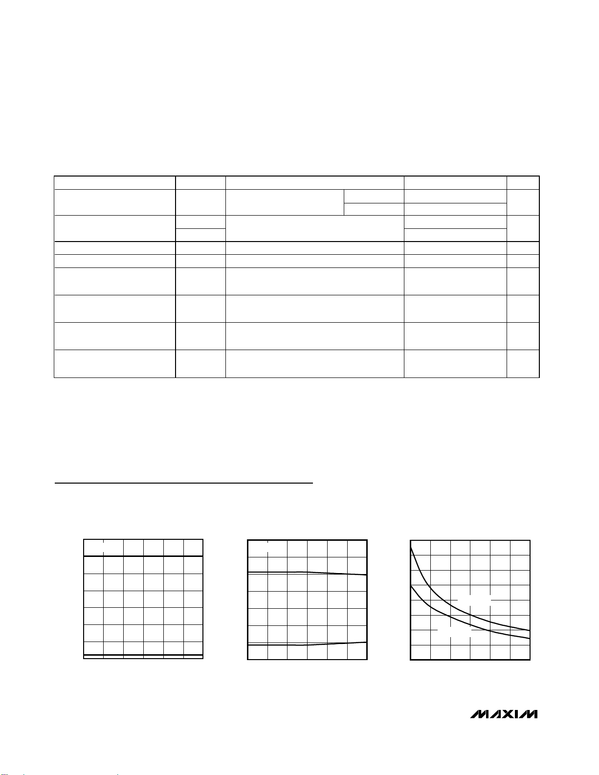
-6
-2
-4
2
0
6
4
8
0 1000 1500500 2000 2500 3000
TRANSMITTER OUTPUT VOLTAGE
vs. LOAD CAPACITANCE
MAX3380E toc01
LOAD CAPACITANCE (pF)
TRANSMITTER OUTPUT VOLTAGE (V)
V
OUT+
V
OUT-
VCC = +4.2V
-6
-2
-4
2
0
6
4
8
0 1000 1500500 2000 2500 3000
TRANSMITTER OUTPUT VOLTAGE
vs. LOAD CAPACITANCE
MAX3380E toc02
LOAD CAPACITANCE (pF)
TRANSMITTER OUTPUT VOLTAGE (V)
V
OUT+
V
OUT-
VCC = +2.5V
0
5
10
15
20
25
30
35
40
0 1000500 1500 2000 2500 3000
MAX3380E
SLEW RATE vs. LOAD CAPACITANCE
MAX3380E toc03
LOAD CAPACITANCE (pF)
SLEW RATE (V/µs)
VCC = +4.2V
VCC = +2.5V
Typical Operating Characteristics
(VCC= VL= +4.2V, C1 = 0.22µF, C2 = C3 = C4 = 1µF, C5 = 0.1µF parallel with 47µF, RL= 3kΩ, CL= 1000pF, data rate is 250kbps,
TA= +25°C, unless otherwise noted.)
MAX3380E/MAX3381E
+2.35V to +5.5V, 1µA, 2Tx/2Rx RS-232 Transceivers
with ±15kV ESD-Protected I/O and Logic Pins
4 _______________________________________________________________________________________
TIMING CHARACTERISTICS
(VCC= +2.35V to +5.5V, VL= +1.65V to +5.5V. When VCC< +4.5V, C1 = C2 = C3 = C4 = 0.1µF; when VCC≥ +4.5V, C1 = 0.047µF,
C2 = C3 = C4 = 0.33µF; T
A
= T
MIN
to T
MAX
, unless otherwise noted. Typical values are at VCC= VL= +3.3V, TA= +25°C.)
Note 2: Transmitter skew is measured at the transmitter zero crosspoint.
PARAMETER SYMBOL CONDITIONS MIN TYP MAX
Maximum Data Rate
Receiver Propagation Delay
Transmitter Skew t
Receiver Skew t
Transition Region Slew Rate
(MAX3380E)
Transition Region Slew Rate
(MAX3381E)
Transition Region Slew Rate
(MAX3380E)
Transition Region Slew Rate
(MAX3381E)
UNITS
MAX3381E 250
MAX3380E 460
20 100 V/µs
6 30 V/µs
kbps
0.15
0.15
30 V/µs
10 V/µs
PHL
PHL
R
= 3kΩ, CL = 1000pF, one
L
transmitter switching
t
PLH
t
PHL
- t
- t
Receiver input to receiver output, CL = 100pF
(Note 2) 200 ns
PLH
50 ns
PLH
VCC = +4.2V, -3.0V < T_OUT< +3.0V,
= 3kΩ, CL = 250pF to 1000pF, TA = +25°C
R
L
VCC = +4.2V, -3.0V < T_OUT< +3.0V,
= 3kΩ, CL = 150pF to 1000pF, TA = +25°C
R
L
VCC = +2.35V, -3.0V < T_OUT< +3.0V,
= 3kΩ, CL = 250pF to 1000pF, TA = +25°C
R
L
VCC = +2.35V, -3.0V < T_OUT< +3.0V,
R
= 3kΩ, CL = 250pF to 1000pF, TA = +25°C
L
µs
Page 5
MAX3380E/MAX3381E
+2.35V to +5.5V, 1µA, 2Tx/2Rx RS-232 Transceivers
with ±15kV ESD-Protected I/O and Logic Pins
_______________________________________________________________________________________ 5
Typical Operating Characteristics (continued)
(VCC= VL= +4.2V, C1 = 0.22µF, C2 = C3 = C4 = 1µF, C5 = 0.1µF parallel with 47µF, RL= 3kΩ, CL= 1000pF, data rate is 250kbps,
T
A
= +25°C, unless otherwise noted.)
SLEW RATE vs. LOAD CAPACITANCE
MAX3381E
14
13
12
11
10
9
SLEW RATE (V/µs)
8
7
6
0 1000500 1500 2000 2500 3000
VCC = +4.2V
VCC = +2.5V
LOAD CAPACITANCE (pF)
TRANSMITTER OUTPUT VOLTAGE
vs. SUPPLY VOLTAGE (V
8
6
V
OUT+
4
2
MAX3380E toc04
SUPPLY CURRENT vs. LOAD CAPACITANCE
WHEN TRANSMITTING DATA
80
1 TRANSMITTER SWITCHING
70
60
50
40
30
SUPPLY CURRENT (mA)
20
10
0
01000500 1500 2000 2500 3000
LOAD CAPACITANCE (pF)
RISING)
CC
MAX3380E toc07
460kbps
MAX3381E toc05
250kbps
20kbps
SUPPLY CURRENT
vs. SUPPLY VOLTAGE (V
25
1 TRANSMITTER SWITCHING
20
15
TRANSMITTER OUTPUT VOLTAGE
vs. SUPPLY VOLTAGE (V
8
6
V
OUT+
4
2
0
-2
V
OUT-
TRANSMITTER OUTPUT VOLTAGE (V)
-4
-6
2.5 3.5 4.5 5.5
FALLING)
CC
SUPPLY VOLTAGE (V)
CC
MAX3380E toc08
FALLING)
MAX3380E toc06
0
-2
V
TRANSMITTER OUTPUT VOLTAGE (V)
OUT-
-4
-6
2.5 3.5 4.5 5.5
SUPPLY VOLTAGE (V)
MAX3380E
1µs/div
= +4.2V
CC
DATASTREAM V
T_IN
5V/div
T_OUT
5V/div
MAX3380E toc09
5V
0
5V
0
-5V
10
SUPPLY CURRENT (mA)
5
0
2.5 3.5 4.5 5.5
SUPPLY VOLTAGE (V)
MAX3380E
1µs/div
= +2.5V
CC
T_IN
5V/div
T_OUT
5V/div
DATASTREAM V
VCC = V
+2.5V
L =
MAX3380E toc10
5V
0
5V
0
-5V
Page 6

MAX3380E/MAX3381E
+2.35V to +5.5V, 1µA, 2Tx/2Rx RS-232 Transceivers
with ±15kV ESD-Protected I/O and Logic Pins
6 _______________________________________________________________________________________
Detailed Description
The MAX3380E/MAX3381E are RS-232 transceivers that
maximize battery life by reducing current consumption
at low battery levels. When the supply voltage is above
+3.7V, the RS-232 outputs are at ±5.5V, which is compliant with the RS-232 standard. As the supply voltage
drops below the +3.1V set point, the RS-232 outputs
change to ±3.7V, which is compatible with the RS-232
standard. The outputs will remain at the compatible levels until the supply voltage rises above +3.5V, where
they return to compliant levels. 400mV of hysteresis protects against power-supply bounce that may cause
numerous mode changes.
Most devices that use charge pumps to double and
invert voltages consume higher current when the supply
voltage is less than half of the required output voltage.
This is due to the fact that the charge pump is constantly operating because the output voltage is below the
regulation voltage. This requires more supply current
because the output will never reach the regulation voltage and switch off. The MAX3380E/MAX3381E reduce
the output voltage requirement allowing the charge
pump to operate with supply voltages down to +2.35V.
Dual-Mode Regulated Charge-Pump
Voltage Converter
The MAX3380E/MAX3381Es’ internal power supply is a
dual-mode regulated charge pump. The output regulation point depends on VCCand the direction in which
VCCmoves through the switchover region of +2.95V <
VCC< +3.7V.
For supply voltages above +3.7V, the charge pump will
generate +5.5V at V+ and -5.5V at V-. The charge
pumps operate in a discontinuous mode. If the output
voltages are less than ±5.5V, the charge pumps are
enabled; if the output voltages exceed ±5.5V, the
charge pumps are disabled.
For supply voltages below +2.95V, the charge pump
will generate +4.0V at V+ and -4.0V at V-. The charge
pumps operate in a discontinuous mode.
Each charge pump requires a flying capacitor (C1, C2)
and a reservoir capacitor (C3, C4) to generate the V+
and V- supplies (see Typical Operating Circuit).
Pin Description
PIN NAME FUNCTION
1 C1+ Positive Terminal of Voltage-Doubler Charge-Pump Capacitor —
2 V+ +5.5V/+4.0V Generated by the Charge Pump —
3 C1- Negative Terminal of Voltage-Doubler Charge-Pump Capacitor —
4 C2+ Positive Terminal of Inverting Charge-Pump Capacitor —
5 C2- Negative Terminal of Inverting Charge-Pump Capacitor —
6 V- -5.5V/-4.0V Generated by the Charge Pump —
7 INVALID
8, 9 T_IN TTL/CMOS Transmitter Inputs Referenced to VL (T1IN, T2IN) ✔
10, 11 R_OUT TTL/CMOS Receiver Outputs Referenced to VL (R2OUT, R1OUT) ✔
12 FORCEON
13 V
14, 15 R_IN RS-232 Receiver Inputs (R2IN, R1IN) ✔
16, 17 T_OUT RS-232 Transmitter Outputs (T2OUT, T1OUT) ✔
18 GND Ground —
19 FORCEOFF
20 V
CC
INVALID is asserted if any inputs of the receivers are in an invalid state;
-0.3V < V
Force-On Input. Drive high to override automatic circuitry keeping transmitters on
(FORCEOFF must be high) (Table 1).
Logic Level Supply. +1.65V to +5.5V, sets CMOS logic thresholds and CMOS
L
outputs.
Force-Off Input. Drive low to shut down transmitters and on-board power supply.
This overrides all automatic circuitry and FORCEON (Table 1).
+2.35V to +5.5V Supply Voltage
R_IN
< +0.3V
ESD
PROTECTED
—
✔
—
✔
—
Page 7

MAX3380E/MAX3381E
+2.35V to +5.5V, 1µA, 2Tx/2Rx RS-232 Transceivers
with ±15kV ESD-Protected I/O and Logic Pins
_______________________________________________________________________________________ 7
Voltage Generation in the
Switchover Region
The MAX3380E/MAX3381E include a switchover circuit
between RS-232-compliant and RS-232-compatible
modes that has approximately 400mV of hysteresis
around the switchover point. The hysteresis is shown in
Figure 1. This large hysteresis helps to avoid mode
change under battery or power-supply bounce.
Under a decaying VCC, the charge pump will generate
an output voltage of ±5.5V with a VCCinput range
between +3.1V and +5.5V. When VCCdrops below the
switchover point of +3.1V, the charge pump switches
into RS-232-compatible mode generating ±4V.
When VCCis rising, the charge pump will generate an
output voltage of ±4.0V, while VCCis between +2.5V
and +3.5V. When VCCrises above the switchover voltage of +3.5V, the charge pump switches to RS-232compliant mode to generate an output voltage of ±5.5V.
RS-232 Transmitters
The transmitters are inverting level translators that convert CMOS-logic levels to RS-232-compatible levels.
The MAX3380E/MAX3381E will automatically reduce
the RS-232-compliant levels from ±5.5V to ±3.7V when
VCCfalls below approximately +3.1V. The reduced levels are RS-232-compatible and reduce supply current
requirements that help preserve the battery. Built-in
hysteresis of approximately 400mV for VCCensures
that the RS-232 output levels do not change if VCCis
noisy or has a sudden current draw causing the supply
voltage to drop slightly. The outputs will return to RS232-compliant levels (±5.5V) when VCCrises above
approximately +3.5V.
The MAX3380E/MAX3381E transmitters guarantee a data
rate of 460kbps/250kbps, respectively, with worst-case
loads of 3kΩ in parallel with 1000pF. Transmitters can be
paralleled to drive multiple receivers.
When FORCEOFF is driven to ground, the transmitters
are disabled and the outputs go into high impedance;
receivers remain active. When the AutoShutdown Plus
circuitry senses that all receiver and transmitter inputs
are inactive for more than 30s, the transmitters are disabled and the outputs go into a high-impedance state,
and the receivers remain active. When the power is off,
the MAX3380E/MAX3381E permit the outputs to be driven up to ±12V.
The transmitter inputs have a 400kΩ active positive
feedback resistor. They will retain a valid logic level if
the driving signal is removed or goes high impedance.
Connect unused transmitter inputs to VCCor ground.
RS-232 Receivers
The receivers convert RS-232 signals to logic levels
referred to VL. Both receivers are active in shutdown
(Table 1).
AutoShutdown Plus Mode
The MAX3380E/MAX3381E achieve a 1µA supply current
with Maxim’s AutoShutdown Plus feature, which operates
when FORCEOFF is high and FORCEON is low. When
these devices do not sense a valid signal transition on
any receiver and transmitter input for 30s, the on-board
charge pumps are shut down, reducing supply current
to 1µA. This occurs if the RS-232 cable is disconnected
or if the connected peripheral transmitters are turned off,
and if the UART driving the transmitter inputs is inactive.
The system turns on again when a valid transition is
applied to any RS-232 receiver or transmitter input. As a
result, the system saves power without changes to the
existing BIOS or operating system.
Figures 2a and 2b show valid and invalid RS-232
receiver voltage levels. INVALID indicates the receiver
input’s condition, and is independent of the FORCEON
and FORCEOFF states. Figure 2 and Table 1 summa-
rize the MAX3380E/MAX3381E’s operating modes.
FORCEON and FORCEOFF override AutoShutdown
Plus circuitry. When neither control is asserted, the IC
selects between these states automatically based on
the last receiver or transmitter input edge received.
By connecting FORCEON to INVALID, the MAX3380E/
MAX3381E is shut down when no valid receiver level and
no receiver or transmitter edge is detected for 30s, and
wakes up when a receiver or transmitter edge is detected (Figure 2c).
Figure 1. V+ Switchover for Changing Vcc
V
CC
2V/div
V+
2V/div
20ms/div
+4.5V
+2.5V
+5.8V
+4.4V
Page 8

MAX3380E/MAX3381E
+2.35V to +5.5V, 1µA, 2Tx/2Rx RS-232 Transceivers
with ±15kV ESD-Protected I/O and Logic Pins
8 _______________________________________________________________________________________
Figure 2a. I
NVALID
Functional Diagram, I
NVALID
Low
Figure 2b. I
NVALID
Functional Diagram, I
NVALID
High
Table 1. AutoShutdown Plus Truth Table
X = Don’t care
OPERATION
STATUS
Shutdown
(Forced Off)
VALID
FORCEON FORCEOFF
X 0 X X High-Z Active
RECEIVER
LEVEL
RECEIVER OR
TRANSMITTER EDGE
WITHIN 30s
T_OUT R_OUT
Normal Operation
(Forced On)
Normal Operation
(AutoShutdown
Plus)
Shutdown
(AutoShutdown
Plus)
Normal Operation INVALID 1 Yes X Active Active
Normal Operation INVALID 1 X Yes Active Active
Shutdown INVALID 1 No No High-Z Active
Normal Operation
(AutoShutdown)
Shutdown
(AutoShutdown)
+0.3V
1 1 X X Active Active
0 1 X Yes Active Active
0 1 X No High-Z Active
INVALID INVALID Yes X Active Active
INVALID INVALID No X High-Z Active
+2.7V
R_IN
-0.3V
INVALID ASSERTED IF ALL RECEIVER INPUTS ARE BETWEEN +0.3V AND -0.3V FOR
AT LEAST 30µs.
30µs
TIMER
R
INVALID
R_IN
-2.7V
INVALID DEASSERTED IF ANY RECEIVER INPUT HAS BEEN BETWEEN +2.7V AND -2.7V
FOR LESS THAN 30µs.
0.3µs
TIMER
R
INVALID
Page 9

MAX3380E/MAX3381E
+2.35V to +5.5V, 1µA, 2Tx/2Rx RS-232 Transceivers
with ±15kV ESD-Protected I/O and Logic Pins
_______________________________________________________________________________________ 9
By connecting FORCEON and FORCEOFF to INVALID,
the MAX3380E/MAX3381E are shut down when no valid
receiver level is detected.
VLLogic Supply Input
Unlike other RS-232 interface devices where the receiver outputs swing between 0 and VCC, the MAX3380E/
MAX3381E feature a separate logic supply input (VL)
that sets VOHfor the receiver and INVALID outputs. V
L
also sets the threshold for the transmitter inputs,
FORCEON and FORCEOFF. This feature allows a great
deal of flexibility in interfacing to many different types of
systems with different logic levels. Connect this input to
Figure 2d. Power-Down Logic
Figure 2c. AutoShutdown Plus Logic
Figure 4. AutoShutdown Plus/
INVALID
Timing Diagram
Figure 3. AutoShutdown Trip Levels
EDGE
T_IN
DETECT
EDGE
R_IN
DETECT
FORCEON
TRANSMITTERS ENABLED, INVALID HIGH
+2.7V
+0.3V
-0.3V
-2.7V
AutoShutdown, TRANSMITTERS DISABLED,
0
TRANSMITTERS ENABLED, INVALID HIGH
INDETERMINATE
1µA SUPPLY CURRENT INVALID LOW
INDETERMINATE
FORCEOFF
S
30s
TIMER
R
AUTOSHDN
FORCEOFF
FORCEON
AUTOSHDN
* POWERDOWN IS ONLY AN INTERNAL SIGNAL.
IT CONTROLS THE OPERATIONAL STATUS OF
THE TRANSMITTERS AND THE POWER SUPPLIES.
POWERDOWN*
RECEIVER
INPUTS
TRANSMITTER
INPUTS
TRANSMITTER
OUTPUTS
INVALID
OUTPUT
V
L
t
INVL
0
V+
V
CC
0
V-
t
INVH
t
AUTOSHDN
INVALID
}
REGION
t
t
WU
AUTOSHDN
t
WU
Page 10

MAX3380E/MAX3381E
the host logic supply (+1.65V to +5.5V). The VLinput
will draw a maximum current of 20µA with receiver outputs unloaded.
±15kV ESD Protection
Maxim has developed state-of-the-art structures to protect these pins against an ESD of ±15kV without damage. The ESD structures withstand high ESD in all states:
normal operation, shutdown, and power-down. After an
ESD event, Maxim’s “E” version devices keep working
without latch-up, whereas competing RS-232 products
can latch and must be powered down to remove latchup. ESD protection can be tested in various ways. The
transmitter and receiver outputs and receiver and logic
inputs of this product family are characterized for protection to the following limits:
• ±15kV using the Human Body Model
• ±8kV using the Contact Discharge method speci-
fied in IEC 1000-4-2
• ±15kV using IEC 1000-4-2’s Air-Gap Discharge
method
ESD Test Conditions
ESD performance depends on a variety of conditions.
Contact Maxim for a reliability report that documents
test setup, methodology, and results.
Human Body Model
Figure 5a shows the Human Body Model, and Figure
5b shows the current waveform it generates when discharged into a low impedance. This model consists of
a 100pF capacitor charged to the ESD voltage of interest, which is then discharged into the test device
through a 1.5kΩ resistor.
IEC 1000-4-2
The IEC 1000-4-2 standard covers ESD testing and
performance of finished equipment; it does not specifically refer to ICs. The MAX3380E/MAX3381E help you
design equipment that meets Level 4, the highest level
of IEC 1000-4-2 without the need for additional ESDprotection components. The major difference between
tests done using the Human Body Model and IEC
1000-4-2 is higher peak current in IEC 1000-4-2,
because series resistance is lower in the IEC 1000-4-2
model. Hence, the ESD withstand voltages measured
+2.35V to +5.5V, 1µA, 2Tx/2Rx RS-232 Transceivers
with ±15kV ESD-Protected I/O and Logic Pins
10 ______________________________________________________________________________________
Figure 5a. Human Body ESD Test Model
Figure 6a. IEC 1000-4-2 ESD Test Model
Figure 5b. Human Body Current Waveform
Figure 6b. IEC 1000-4-2 ESD Generator Current Waveform
R
D
1500Ω
DISCHARGE
RESISTANCE
STORAGE
CAPACITOR
DEVICE
UNDER
TEST
HIGH-
VOLTAGE
DC
SOURCE
R
C
1MΩ
CHARGE-CURRENT
LIMIT RESISTOR
C
s
100pF
IP 100%
90%
AMPERES
36.8%
10%
0
0
t
RL
TIME
t
DL
CURRENT WAVEFORM
PEAK-TO-PEAK RINGING
I
r
(NOT DRAWN TO SCALE)
R
D
330Ω
DISCHARGE
RESISTANCE
STORAGE
CAPACITOR
HIGH-
VOLTAGE
DC
SOURCE
R
C
50MΩ to 100MΩ
CHARGE-CURRENT
LIMIT RESISTOR
C
s
150pF
I
100%
90%
PEAK
I
10%
tr = 0.7ns to 1ns
30ns
60ns
DEVICE
UNDER
TEST
t
Page 11

MAX3380E/MAX3381E
+2.35V to +5.5V, 1µA, 2Tx/2Rx RS-232 Transceivers
with ±15kV ESD-Protected I/O and Logic Pins
______________________________________________________________________________________ 11
to IEC 1000-4-2 are generally lower than that measured
using the Human Body Model. Figure 6a shows the IEC
1000-4-2 model, and Figure 6b shows the current
waveform for the ±8kV IEC 1000-4-2 Level 4 ESD
Contact Discharge test.
The Air-Gap test involves approaching the device with
a charged probe. The Contact Discharge method connects the probe to the device before the probe is energized.
Machine Model
The Machine Model for ESD tests all pins using a
200pF storage capacitor and zero discharge resistance. Its objective is to emulate the stress caused by
contact that occurs with handling and assembly during
manufacturing. All pins require this protection during
manufacturing, not just RS-232 inputs and outputs.
Therefore, after PC board assembly, the Machine
Model is less relevant to I/O ports.
Applications Information
Capacitor Selection
The capacitor type used for C1–C4 is not critical for
proper operation. Polarized or nonpolarized capacitors
can be used. The charge pump requires 0.1µF capacitors for +3.3V operation. For other supply voltages, see
Table 2 for required capacitor values. Do not use values smaller than those listed in Table 2. Increasing the
capacitor values (e.g., by a factor of 2) reduces ripple
on the transmitter outputs and slightly reduces power
consumption. C2, C3, and C4 can be increased without
changing C1’s value. However, do not increase C1
without also increasing the values of C2, C3, C4, and
C5 to maintain the proper ratios (C1 to the other capacitors).
When using the minimum required capacitor values,
make sure the capacitor value does not degrade
excessively with temperature. If in doubt, use capacitors with a large nominal value. The capacitor’s equivalent series resistance (ESR) usually rises at low
temperatures and influences the amount of ripple on
V+ and V-.
Power-Supply Decoupling
In most circumstances, connect a 0.1µF capacitor from
VCCto GND. This capacitor is for noise reduction. If the
MAX3380E/MAX3381E are used in a data cable application, add a 47µF capacitor from VCCto ground. The
47µF capacitor is used to ensure that the current needed during power-up is supplied to the device. In applications that are sensitive to power-supply noise,
decouple VCCto ground with a capacitor of the same
value as charge-pump capacitor C1. Connect bypass
capacitors as close to the IC as possible.
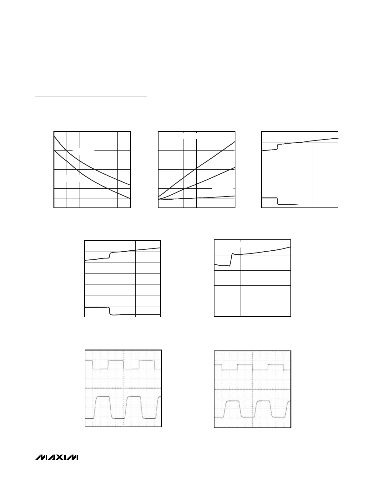
Transmitter Outputs when Recovering
from Shutdown
Figure 7 shows two transmitter outputs when exiting
shutdown mode. As they become active, the two transmitter outputs are shown going to opposite RS-232 levels (one transmitter input is high, the other is low). Each
transmitter is loaded with 3kΩ in parallel with 1000pF.
The transmitter outputs display no ringing or undesirable transients as they come out of shutdown. Note that
the transmitters are enabled only when the magnitude
of V- exceeds approximately 3V.
High Data Rates
The MAX3380E/MAX3381E maintain the RS-232 ±5.0V
minimum transmitter output voltage even at high data
rates. Figure 8 shows a transmitter loopback test circuit. Figure 9 shows a loopback test result for the
MAX3380E at 460kbps with true RS-232 output voltage
levels (VCC= +4.2V). Figure 10 shows the same test
with RS-232-compatible levels (VCC= +2.5V). With
data rates as high as 460kbps, the MAX3380E is compatible with 2.5-Generation GSM standards.
Table 2. Minimum Required Capacitor
Values
Figure 7. Transmitter Outputs when Recovering from Shutdown
or Powering Up
FORCEON =
5V
0
5V/div
2V/div
6V
0
FORCEOFF
T2OUT
VCC (V) C1, C5 (µF) C2, C3, C4 (µF)
+2.35 to +3.6 0.1 0.1
+4.5 to +5.5 0.047 0.33
+2.35 to +5.5 0.22 1
T1OUT
6V
4µs/div
VCC = 3.3V, C1–C4 = 0.1µF, C
LOAD
= 1000pF
Page 12

MAX3380E/MAX3381E
+2.35V to +5.5V, 1µA, 2Tx/2Rx RS-232 Transceivers
with ±15kV ESD-Protected I/O and Logic Pins
12 ______________________________________________________________________________________
For Figure 9 and Figure 10, a single transmitter was driven at 460kbps, and all transmitters were loaded with
an RS-232 receiver in parallel with 1000pF.
Data Cable Applications
The MAX3380E/MAX3381Es’ ±15kV ESD protection on
both the RS-232 I/Os as well as the logic I/Os makes
them ideal candidates for data cable applications. A
data cable is both an electrical connection and a level
translator, allowing ultra-miniaturization of cell phones
and other small portable devices.
Previous data cable approaches suffered from complexity due to the required protection circuits on both
the logic side of the cable, as well as on the RS-232
connections. The example shown in Figure 11 shows
the ease of using the MAX3380E/MAX3381E in data
cable applications. For best performance, keep the
logic level lines short and use the RS-232 level lines to
span any distance.
Figure 10. Loopback Test Results at 460kbps (VCC= +2.5V)
Figure 9. Loopback Test Results at 460kbps (VCC= +4.2V)
Figure 8. Loopback Test Circuit
V
C1
C2
CC
C5
V
V
CC
C1+
C1-
C2+
C2-
MAX3380E
MAX3381E
L
V+
C3
V-
C4
T1IN
5V/div
T1OUT
5V/div
R1OUT
5V/div
1µs/div
VCC = V
+4.2V, C1 = 0.1µF, C2 = C3 = C4 = 1µF,
L =
= 1000pF
C
LOAD
T1IN
2V/div
T1OUT
5V/div
R1OUT
2V/div
5V
0
5V
0
-5V
5V
0
2V
0
5V
0
-5V
2V
0
T_ IN
R_ OUT
FORCEON
V
CC
FORCEOFF
GND
T_ OUT
R_ IN
5kΩ
1000pF
VCC = V
C
LOAD
TIME (1µs/div)
+2.5V, C1 = 0.1µF, C2 = C3 = C4 = 1µF,
L =
= 1000pF
Page 13

MAX3380E/MAX3381E
+2.35V to +5.5V, 1µA, 2Tx/2Rx RS-232 Transceivers
with ±15kV ESD-Protected I/O and Logic Pins
______________________________________________________________________________________ 13
Figure 11. Typical Application Circuit
Chip Information
TRANSISTOR COUNT: 1467
PROCESS: BiCMOS
20
19
18
17
16
15
14
13
1
2
3
4
5
6
7
8
V
CC
FORCEOFF
GND
T1OUTC2+
C1-
V+
C1+
TOP VIEW
T2OUT
R1IN
R2IN
V
L
T1IN
INVALID
V-
C2-
12
11
9
10
FORCEON
R1OUTR2OUT
T2IN
MAX3380E/
MAX3381E
TSSOP
Pin Configuration
0.1µF47µF
V
BATT
CELL PHONE
LOGIC LEVELS
Tx
RTS
Rx
CTS
0.1µF
0.1µF
V
C1+
C1-
C2+
C2-
T1IN
T2IN
R1OUT
R2OUT
CC
MAX3380E/
MAX3381E
V
L
FORCEOFF
FORCEON
T1OUT
T2OUT
R1IN
R2IN
INVALID
V+
V-
0.1µF
0.1µF
PERIPHERALS
RS-232 LEVELS
Tx
CTS
Rx
RTS
I/O
Page 14

MAX3380E/MAX3381E
+2.35V to +5.5V, 1µA, 2Tx/2Rx RS-232 Transceivers
with ±15kV ESD-Protected I/O and Logic Pins
Maxim cannot assume responsibility for use of any circuitry other than circuitry entirely embodied in a Maxim product. No circuit patent licenses are
implied. Maxim reserves the right to change the circuitry and specifications without notice at any time.
14 ____________________Maxim Integrated Products, 120 San Gabriel Drive, Sunnyvale, CA 94086 408-737-7600
© 2001 Maxim Integrated Products Printed USA is a registered trademark of Maxim Integrated Products.
Package Information
TSSOP.EPS
 Loading...