

Page 1
现货库存、技术资料、百科信息、热点资讯,精彩尽在鼎好!
General Description
The MAX3370/MAX3371 logic level translators are ideal
for applications interfacing low-voltage devices to other
logic levels. Externally applied voltages set the logic
levels of the MAX3370/MAX3371. The devices accept
VCCfrom +2.5V to +5.5V and VLfrom +1.6V to +5.5V,
allowing data transfer between low-voltage ASICs and
higher voltage devices. The MAX3371 features a shutdown mode that reduces supply current to <1µA and
puts the I/O pins in a high-impedance state.
The MAX3370/MAX3371 are bidirectional level shifters,
allowing data transfer from the VCCside to the VLside
and from the VLside to the VCCside. Both devices
operate at speeds up to 2Mbps with an active driver
and up to 500kbps with an open-drain driver.
The MAX3370/MAX3371 are available in space-saving
5-pin and 6-pin SC70 packages, respectively.
________________________Applications
Cell Phone Cradles
Cell Phone Hands-Free Kits
Portable POS Systems
Portable Communication Devices
Smart Card Readers
SPI™, MICROWIRE™, and I2C™ Level Translation
Low-Voltage ASIC Level Translation
RS-232-Compatible Translation
Features
♦ Allow Bidirectional Level Translation
♦ Miniature SC70 Packages
♦ Operational Down to 1.6V
♦ Low Quiescent Current (<100µA)
♦ Ultra-Low (<1µA) Shutdown Supply Current
(MAX3371)
♦ Three-State Outputs in Shutdown (MAX3371)
♦ 2Mbps (10pF Load) Push-Pull Driving
♦ 1Mbps (50pF Load) Push-Pull Driving
♦ 500kbps (30pF Load) Open-Drain Driving
MAX3370/MAX3371
†
1µA, 2Mbps, Low-Voltage Level
Translators in SC70
________________________________________________________________ Maxim Integrated Products 1
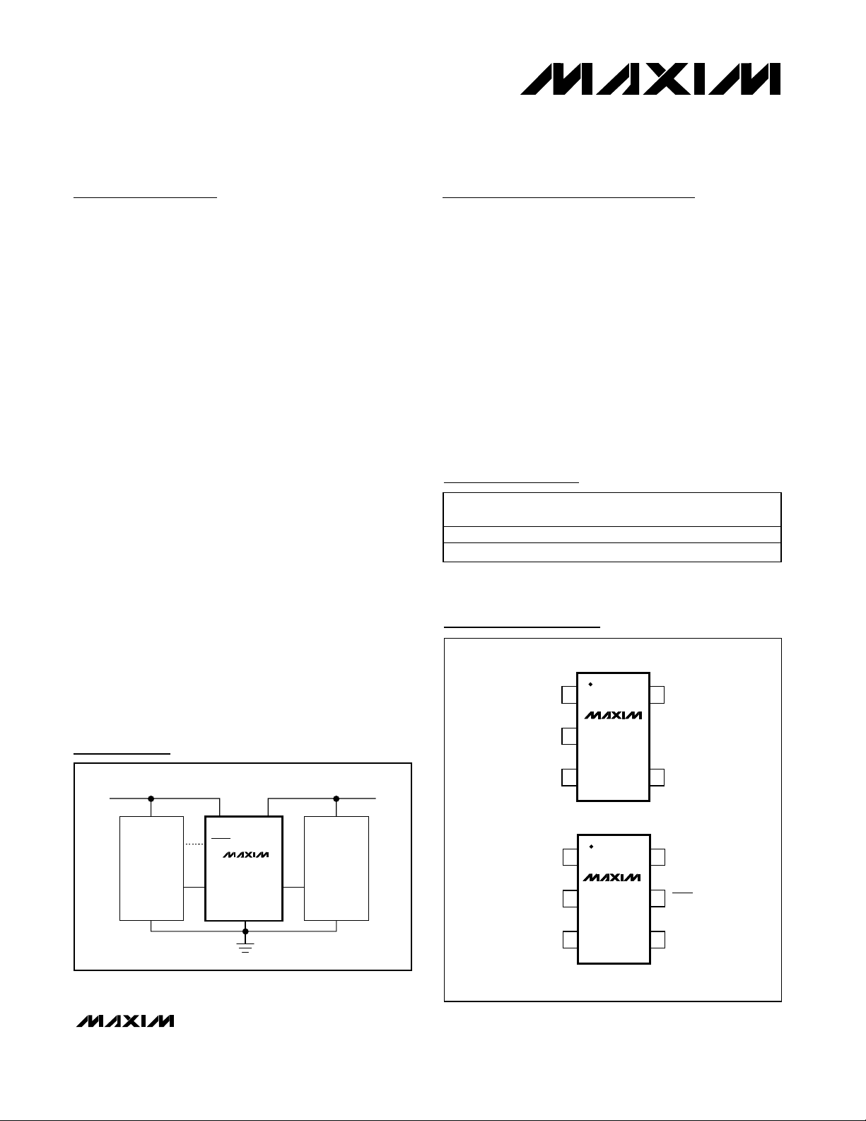
GND
I/O V
CC
I/O V
L
15V
CC
V
L
MAX3370
SC70-5
TOP VIEW
2
34
GND
I/O V
CC
I/O V
L
16V
CC
5 SHDN
V
L
MAX3371
SC70-6
2
34
Pin Configurations
DATA I/O VLI/O V
CC
1.8V
SYSTEM
CONTROLLER
+1.8V +3.3V
3.3V SYSTEM
V
L
SHDN
*
V
CC
DATA
GNDGND
*
MAX3371 ONLY
GND
MAX3370
MAX3371
Typical Operating Circuit
19-1847; Rev 1; 2/01
Ordering Information
I2C is a trademark of Philips Corp.
SPI is a trademark of Motorola, Inc.
MICROWIRE is a trademark of National Semiconductor Corp.
PART
TEMP.
RANGE
PIN-
TOP
MARK
MAX3370EXK-T
ABV
MAX3371EXT-T
AAO
For price, delivery, and to place orders, please contact Maxim Distribution at 1-888-629-4642,
or visit Maxim’s website at www.maxim-ic.com.
†
MAX3370/MAX3371 covered by U.S. Patent number 5,894,240.
PACKAGE
-40°C to +85°C 5 SC70-5 NO
-40°C to +85°C 6 SC70-6 YES
SHDN
Page 2
MAX3370/MAX3371
1µA, 2Mbps, Low-Voltage Level
Translators in SC70
2 _______________________________________________________________________________________
ABSOLUTE MAXIMUM RATINGS
ELECTRICAL CHARACTERISTICS
(VCC= +2.5V to +5.5V, VL= +1.6V to +5.5V (Note 1), GND = 0; I/O VL, I/O VCCunconnected; TA= -40°C to +85°C, unless otherwise
noted. Typical values are at T
A
= +25°C.) (Note 2)
Stresses beyond those listed under “Absolute Maximum Ratings” may cause permanent damage to the device. These are stress ratings only, and functional
operation of the device at these or any other conditions beyond those indicated in the operational sections of the specifications is not implied. Exposure to
absolute maximum rating conditions for extended periods may affect device reliability.
VCCto GND..............................................................-0.3V to +7V
SHDN to GND...............................................-0.3V to (VL+ 0.3V)
I/O V
L
to GND................................................-0.3V to (VL+ 0.3V)
VL, I/O VCCto GND...................................-0.3V to (VCC+ 0.3V)
Short-Circuit Duration: I/O VL, I/O VCCto GND..........Continuous
Continuous Power Dissipation (T
A
= +70°C)
5/6-Pin SC70 (derate 3.1mW/°C above +70°C) ...........245mW
Operating Temperature Range ...........................-40°C to +85°C
Storage Temperature Range.............................-65°C to +150°C
Lead Temperature (soldering, 10s).................................+300°C
PARAMETER
CONDITIONS
UNITS
POWER SUPPLIES
VL Supply Range V
L
(Note 1) 1.6 5.5 V
VCC Supply Range V
CC
2.5 5.5 V
Supply Current from V
CC
70 100 µA
Supply Current from V
L
I
QVL
5 100 µA
V
CC
Shutdown Supply Current SHDN = GND, TA = +25°C, MAX3371
1 µA
VL Shutdown Supply Current SHDN = GND, TA = +25°C, MAX3371
1 µA
Three-State Output Leakage
Current
I/O VL, I/O VCC; SHDN = GND, TA = +25°C,
MAX3371
1 µA
LOGIC LEVEL THRESHOLDS
I/O VL Input Voltage High
Threshold
V
IHL
V
I/O VL Input Voltage Low
Threshold
V
ILL
V
I/O VCC Input Voltage High
Threshold
V
IHC
V
I/O VCC Input Voltage Low
Threshold
V
ILC
0.2 V
I/O VL Output Voltage High V
OHL
I/O VL sink current = 20µA,
I/O V
CC
≥ VCC - 0.4V (Note 3)
V
L
V
I/O VL Output Voltage Low V
OLL
I/O VL sink current = 1mA, I/O V
CC
≤ 0.2V
(Note 3)
0.4 V
I/O VCC Output Voltage High V
OHC
I/O VCC source current = 20µA,
I/O V
L
≥ V
L
- 0.2V (Note 3)
V
I/O VCC Output Voltage Low V
OLC
I/O VCC sink current = 1mA,
I/O V
L
≤ 0.15V (Note 3)
0.4 V
SHDN Input Voltage High
V
L
V
VL ≥ +1.8V 0.4
SHDN Input Voltage Low
VL ≥ +1.6V 0.2
V
SYMBOL
I
V
IH-SHDN
V
IL-SHDN
QVCC
MIN TYP MAX
0.03
0.03
0.02
0.15
2/3 ×
2/3 ×
V
CC
2/3 ×
VL - 0.2
VCC - 0.4
Page 3
MAX3370/MAX3371
1µA, 2Mbps, Low-Voltage Level
Translators in SC70
_______________________________________________________________________________________ 3
ELECTRICAL CHARACTERISTICS (continued)
(VCC= +2.5V to +5.5V, VL= +1.6V to +5.5V (Note 1), GND = 0; I/O VL, I/O VCCunconnected; TA= -40°C to +85°C, unless otherwise
noted. Typical values are at T
A
= +25°C.) (Note 2)
PARAMETER
CONDITIONS
UNITS
T IM IN G C H A RA C T ER ISTIC S ( R
LOAD
= 1M Ω , V
C C
= + 2.5V , VL = + 1.6V , I/O test si g nal Rai l -to- Rai l
®
unless othe r w i se noted , Fi gur e 1) (N ote 3)
C
LOAD
= 10pF, data rate = 2Mbps (Note 5) 100
C
LOAD
= 50pF, data rate = 1Mbps 200
I/O VCC Rise Time
(Note 4)
t
RVCC
C
LOAD
= 30pF, data rate = 500kbps,
open-drain drive
400
ns
C
LOAD
= 10pF, data rate = 2Mbps (Note 5) 50
C
LOAD
= 50pF, data rate = 1Mbps 200
I/O VCC Fall Time
(Note 4)
t
FVCC
C
LOAD
= 30pF, data rate = 500kbps,
open-drain drive
400
ns
C
LOAD
= 10pF, data rate = 2Mbps (Note 5) 100
C
LOAD
= 50pF, data rate = 1Mbps 200
I/O VL Rise Time
(Note 4)
t
RVL
C
LOAD
= 30pF, data rate = 500kbps,
open-drain drive
400
ns
C
LOAD
= 10pF, data rate = 2Mbps (Note 5) 50
C
LOAD
= 50pF, data rate = 1Mbps 200
I/O VL Fall Time
(Note 4)
t
FVL
C
LOAD
= 30pF, data rate = 500kbps,
open-drain drive
400
ns
C
LOAD
= 10pF, data rate = 2Mbps (Note 5) 50
C
LOAD
= 50pF, data rate = 1Mbps 200
HIGH-to-LOW Transition
Propagation Delay
(Driving I/O V
L
)
C
LOAD
= 30pF, data rate = 500kbps,
open-drain drive
400
ns
C
LOAD
= 10pF, data rate = 2Mbps (Note 5) 200
C
LOAD
= 50pF, data rate = 1Mbps 400
LOW-to-HIGH Transition
Propagation Delay
(Driving I/O V
L
)
C
LOAD
= 30pF, data rate = 500kbps,
open-drain drive
800
ns
C
LOAD
= 10pF, data rate = 2Mbps (Note 5) 50
C
LOAD
= 50pF, data rate = 1Mbps 200
HIGH-to-LOW Transition
Propagation Delay
(Driving I/O V
CC
)
C
LOAD
= 30pF, data rate = 500kbps,
open-drain drive
400
ns
C
LOAD
= 10pF, data rate = 2Mbps (Note 5) 200
C
LOAD
= 50pF, data rate = 1Mbps 400
LOW-to-HIGH Transition
Propagation Delay
(Driving I/O V
CC
)
C
LOAD
= 30pF, data rate = 500kbps,
open-drain drive
800
ns
C
LOAD
= 10pF, data rate = 2Mbps (Note 3) 2
C
LOAD
= 50pF, data rate = 1Mbps 4
HIGH-to-LOW Transition
Propagation Delay
Device-to-Device Skew
(Driving I/O V
L
)
C
LOAD
= 30pF, data rate = 500kbps,
open-drain drive
5
ns
Rail-to-Rail is a registered trademark of Nippon Motorola Ltd.
SYMBOL
MIN TYP MAX
t
PD-VCC-HL
t
PD-VCC-LH
t
PD-VL-HL
t
PD-VL-LH
Page 4

MAX3370/MAX3371
1µA, 2Mbps, Low-Voltage Level
Translators in SC70
4 _______________________________________________________________________________________
Note 1: VLmust always be less than or equal to VCC.
Note 2: All units are 100% production tested at T
A
= +25°C. Limits over the operating temperature range are guaranteed by design
and not production tested.
Note 3: Tested only at worst case: V
CC
= +2.5V, VL= +1.6V.
Note 4: 10% to 90%.
Note 5: Guaranteed by correlation to C
LOAD
= 50pF.
ELECTRICAL CHARACTERISTICS (continued)
(VCC= +2.5V to +5.5V, VL= +1.6V to +5.5V (Note 1), GND = 0; I/O VL, I/O VCCunconnected; TA= -40°C to +85°C, unless otherwise
noted. Typical values are at T
A
= +25°C.) (Note 2)
PARAMETER
SYMBOL
CONDITIONS
MIN
TYP
MAX
UNITS
C
LOAD
= 10pF, data rate = 2Mbps (Note 3) 5
C
LOAD
= 50pF, data rate = 1Mbps 8
LOW-to-HIGH Transition
Propagation Delay
Device-to-Device Skew
(Driving I/O V
L
)
C
LOAD
= 30pF, data rate = 500kbps,
open-drain drive
80
ns
C
LOAD
= 10pF, data rate = 2Mbps (Note 3) 2
C
LOAD
= 50pF, data rate = 1Mbps 4
HIGH-to-LOW Transition
Propagation Delay
Device-to-Device Skew
(Driving I/O V
CC
)
C
LOAD
= 30pF, data rate = 500kbps,
open-drain drive
5
ns
C
LOAD
= 10pF, data rate = 2Mbps (Note 3) 7
C
LOAD
= 50pF, data rate = 1Mbps 8
LOW-to-HIGH Transition
Propagation Delay
Device-to-Device Skew
(Driving I/O V
CC
)
C
LOAD
= 30pF, data rate = 500kbps,
open-drain drive
50
ns
C
LOAD
= 10pF (Note 5) 2 3
C
LOAD
= 50pF 1 2Maximum Data Rate
C
LOAD
= 30pF, open-drain drive 0.5 1
Mbps
Page 5

MAX3370/MAX3371
1µA, 2Mbps, Low-Voltage Level
Translators in SC70
_______________________________________________________________________________________ 5
+2.5V+1.6V
GND
I/O V
L
I/O V
L
I/O V
CC
I/O V
CC
VLV
CC
t
PD-VCC-LH
t
PD-VCC-HL
MAX3370
MAX3371
t
RVCC
t
FVCC
DATA
C
LOAD
R
LOAD
t
RISE, tFALL
≤10ns
Figure 1a. Rail-to-Rail Driving I/O V
L
Figure 1b. Rail-to-Rail Driving I/O V
CC
Figure 1c. Open-Drain Driving I/O V
L
Figure 1d. Open-Drain Driving I/O V
CC
+2.5V+1.6V
VLV
CC
MAX3370
MAX3371
DATA
I/O V
I/O V
L
CC
C
LOAD
t
RISE, tFALL
I/O V
I/O V
CC
≤10ns
L
R
LOAD
t
PD-VL-LH
GND
t
PD-VL-HL
t
RVL
t
FVL
I/O V
I/O V
L
t
≤10ns
RISE, tFALL
t
PD-VCC-LH
I/O V
CC
t
RVCC
VLV
MAX3370
MAX3371
L
GND
I/O V
CC
CC
t
PD-VCC-HL
+2.5V+1.6V
DATA
t
FVCC
R
LOAD
C
LOAD
VLV
MAX3370
MAX3371
DATA
I/O V
I/O V
L
C
t
RISE, tFALL
LOAD
I/O V
I/O V
CC
≤10ns
L
R
LOAD
t
PD-VL-LH
GND
t
RVL
CC
CC
+2.5V+1.6V
t
PD-VL-HL
t
FVL
Page 6

MAX3370/MAX3371
1µA, 2Mbps, Low-Voltage Level
Translators in SC70
6 _______________________________________________________________________________________
Typical Operating Characteristics
(Driving I/O VLrail-to-rail, RL= 1MΩ,TA = +25°C, unless otherwise noted.)
I
VL
(µA)
86
88
90
92
94
96
98
100
102
2.5 3.53.0 4.0 4.5 5.0 5.5
VL SUPPLY CURRENT
vs. POWER-SUPPLY VOLTAGE
MAX3370-01
V
CC
(V)
RATE = 2Mbps, C
LOAD
= 10pF
RATE = 1Mbps, C
LOAD
= 50pF
RATE = 500kbps, C
LOAD
= 30pF,
OPEN-DRAIN DRIVE
VL = 1.8V
0
200
100
400
300
500
600
2.5 3.5 4.03.0 4.5 5.0 5.5
MAX3370-02
V
CC
(V)
I
VCC
(µA)
V
CC
SUPPLY CURRENT
vs. POWER-SUPPLY VOLTAGE
RATE = 2Mbps, C
LOAD
= 10pF
RATE = 1Mbps, C
LOAD
= 50pF
VL = 1.8V
RATE = 500kbps, C
LOAD
= 30pF,
OPEN-DRAIN DRIVE
89
92
91
90
93
94
95
96
97
98
99
-40 10-15 356085
MAX3370-03
TEMPERATURE (°C)
I
VL
(µA)
VL SUPPLY CURRENT
vs. TEMPERATURE
VCC = 2.5V
VCC = 3.3V
VCC = 5.0V
VL = 1.8V, RATE = 500kbps,
C
LOAD
= 30pF,
OPEN-DRAIN DRIVE
100
200
150
300
250
400
350
450
-40 10-15 356085
MAX3370-04
TEMPERATURE (°C)
I
VCC
(µA)
V
CC
SUPPLY CURRENT
vs. TEMPERATURE
VCC = 2.5V
VCC = 3.3V
VCC = 5.0V
VL = 1.8V, RATE = 500kbps,
C
LOAD
= 30pF,
OPEN-DRAIN DRIVE
80
90
85
100
95
110
105
115
MAX3370-05
C
LOAD
(pF)
I
VL
(µA)
0 50 100 150 200
VL SUPPLY CURRENT
vs. LOAD CAPACITANCE
RATE = 500kbps, C
LOAD
= 30pF,
OPEN-DRAIN DRIVE
RATE = 2Mbps, C
LOAD
= 10pF
RATE = 1Mbps, C
LOAD
= 50pF
VL = 1.8V
V
CC
= 3.3V
80
280
180
480
380
680
580
780
MAX3370-06
C
LOAD
(pF)
I
VCC
(µA)
0 50 100 150 200
V
CC
SUPPLY CURRENT
vs. LOAD CAPACITANCE
RATE = 500kbps, C
LOAD
= 30pF,
OPEN-DRAIN DRIVE
RATE = 2Mbps, C
LOAD
= 10pF
RATE = 1Mbps, C
LOAD
= 50pF
VL = 1.8V
V
CC
= 3.3V
Page 7

MAX3370/MAX3371
1µA, 2Mbps, Low-Voltage Level
Translators in SC70
_______________________________________________________________________________________ 7
0
15
10
5
20
25
30
35
40
45
50
0 50 100 150 200
MAX3370-07
C
LOAD
(pF)
PROPAGATION DELAY (ns)
PROPAGATION DELAY
vs. LOAD CAPACITANCE (DRIVING I/O V
L
)
LOW-TO-HIGH TRANSITION
HIGH-TO-LOW TRANSITION
VL = 1.8V
V
CC
= 3.3V
0
10
5
20
15
30
25
35
0 50 100 150 200
MAX3370-08
C
LOAD
(pF)
PROPAGATION DELAY (ns)
PROPAGATION DELAY
vs. LOAD CAPACITANCE (DRIVING I/O V
CC
)
LOW-TO-HIGH TRANSITION
HIGH-TO-LOW TRANSITION
VL = 1.8V
V
CC
= 3.3V
I/O V
CC
0
1V/div
0
I/O V
L
100ns/div
RAIL-TO-RAIL DRIVING
(RATE = 2Mbps, C
LOAD
= 10pF,
V
CC
= 3.3V, VL = 1.8V)
MAX3370-09
I/O V
CC
0
1V/div
0
I/O V
L
200ns/div
RAIL-TO-RAIL DRIVING
(RATE = 1Mbps, C
LOAD
= 50pF,
V
CC
= 3.3V, VL = 1.8V)
MAX3370-10
I/O V
CC
0
1V/div
0
I/O V
L
400ns/div
OPEN-DRAIN DRIVING
(RATE = 500kbps, C
LOAD
= 30pF,
V
CC
= 3.3V, VL = 1.8V)
MAX3370-11
I/O V
CC
0
2V/div
0
I/O V
L
400ns/div
OPEN-DRAIN DRIVING
(RATE = 500kbps, C
LOAD
= 30pF,
V
CC
= 5V, VL = 2.5V)
MAX3370-12
0
2V/div
0
I/O V
CC
100ns/div
MAX3371
EXITING SHUTDOWN
MAX3370-13
I/O V
L
V
SHDN
0
Typical Operating Characteristics (continued)
(Driving I/O V
L
rail-to-rail, RL= 1MΩ, TA = +25°C, unless otherwise noted.)
Page 8

MAX3370/MAX3371
1µA, 2Mbps, Low-Voltage Level
Translators in SC70
8 _______________________________________________________________________________________
Pin Description
PIN
MAX3370 MAX3371
NAME FUNCTION
11V
L
Logic Supply Voltage
2 2 GND Ground
3 3 I/O V
L
Input/Output Referred to V
L
4 4 I/O V
CC
Input/Output Referred to V
CC
56V
CC
Power-Supply Voltage
— 5 SHDN
Shutdown. A high turns on the device. A low shuts down the device. I/O V
CC
and I/O VL are high impedance in shutdown.
Detailed Description
The MAX3370/MAX3371 provide the necessary level
translation to allow data transfer in a multivoltage system. These devices transmit data between an I/O pin
referenced to VCCand an I/O pin referenced to VL. The
VCCsupply voltage range is from +2.5V to +5.5V, and
the VLsupply voltage range is between +1.6V and
+5.5V. The MAX3371 features a shutdown mode in
which I/O V
CC
and I/O VL are placed in a high-imped-
ance state and supply current drops to 1µA.
The MAX3370/MAX3371 are bidirectional level shifters
allowing data transfer from the VCCside to the VLside,
and from the VLside to the VCCside. Both devices
operate at speeds up to 2Mbps with an active driver
and up to 500kbps with an open-drain driver.
Level Translation
The MAX3370/MAX3371 provide bidirectional level
translation between I/O pins referred to VCCand VL.
I/O VCCand I/O VLare internally pulled up to their
respective power-supply rails through 10kΩ resistors.
VCCmust be between +2.5V and +5.5V, and VLmust
be between +1.6V and +5.5V. For proper operation, V
L
can not exceed VCC.
The MAX3370/MAX3371 can operate at data rates up
to 2Mbps when driven by an active (push-pull) driver
with a 10pF load, 1Mbps when driven by an active driver with a 50pF load, or 500kbps when driven by an
open-drain driver with a 30pF load. The internal pullups
allow these devices to be driven by open-drain drivers.
MAX3371 Shutdown Mode
The MAX3371 enters a low-power shutdown mode
when SHDN is driven low. Connect SHDN to V
L
or drive
high for normal operation. Activating shutdown mode
disconnects the internal 10kΩ pullup resistors on I/O
V
CC
and I/O VL. As a result, the supply current
decreases to <1µA, and the I/O lines are high impedance. The high impedance I/O lines in shutdown allow
use in a multidrop network. When in shutdown, I/O V
L
can be driven to VLand I/O VCCcan be driven to VCC.
Speed-Up
The speed-up circuit is a one-shot generator that helps
the rise time of the output waveform in the low-to-high
transition. When triggered, switches S1and S2turn on
for 320ns to pull up I/O VLand I/O VCC. This greatly
reduces the rise time and propagation delay for the
low-to-high transition as well as improves the duty
cycle (closer to 50% for an ideal square-wave input).
See the scope plots in the Typical Operating
Characteristics for the speed-up circuitry in operation.
Functional Diagram
SPEEDUP
MNSW
R
1
S
1
S
2
R
2
GND
I/O V
CC
I/O V
L
V
CC
V
L
MAX3370
Page 9

MAX3370/MAX3371
1µA, 2Mbps, Low-Voltage Level
Translators in SC70
_______________________________________________________________________________________ 9
Applications Information
Power-Supply Decoupling
To reduce ripple and the chance of transmitting incorrect data, decouple V
CC
and VL to ground with a 0.1µF
capacitor as close to the device as possible.
I2C Level Translation
The MAX3370/MAX3371 are ideal for level translation
between a low-voltage ASIC and an I
2
C device. The
devices’ bidirectional natures allow their use in the data
line of I
2
C communications. A typical application is
interfacing a low-voltage microprocessor to a 3V or 5V
D/A converter, such as the MAX517.
The I/O lines on the MAX3370/MAX3371 are bidirectional, can be level-shifted up to +5.5V, and contain
internal 10kΩ pullup resistors to allow open-drain dri ving (see the Typical Operating Circuit).
Push-Pull vs. Open-Drain Driving
The MAX3370/MAX3371 I/O pins can be driven by a
push-pull or open-drain device. When using a push-pull
driver, the MAX3370/MAX3371 operate up to 2Mbps
with a 10pF load or 1Mbps with a 50pF load. The internal pullup resistors on the I/O pins allow use with opendrain devices. The MAX3370/MAX3371 operate up to
500kbps with a 30pF load when driven by an opendrain device.
Data rates higher than those listed in the Electrical
Characteristics table can be achieved. The maximum
data rate is limited to 3Mbps by the speed-up circuitry.
Unidirectional vs. Bidirectional Level Translator
The MAX3370/MAX3371 may also be used to translate
unidirectional signals without signal inversion. The
devices provide the smallest solution (SC70 package)
for unidirectional level translation without inversion.
Chip Information
TRANSISTOR COUNT: 75
PROCESS: BiCMOS
Page 10

MAX3370/MAX3371
1µA, 2Mbps, Low-Voltage Level
Translators in SC70
1µA, 2Mbps, Low-Voltage Level
Translators in SC70
Maxim cannot assume responsibility for use of any circuitry other than circuitry entirely embodied in a Maxim product. No circuit patent licenses are
implied. Maxim reserves the right to change the circuitry and specifications without notice at any time.
10 ____________________Maxim Integrated Products, 120 San Gabriel Drive, Sunnyvale, CA 94086 408-737-7600
© 2001 Maxim Integrated Products Printed USA is a registered trademark of Maxim Integrated Products.
Package Information
SC70, 5L.EPS
SC70, 6L.EPS
 Loading...