

Page 1
现货库存、技术资料、百科信息、热点资讯,精彩尽在鼎好!
General Description
The MAX3362 low-power, high-speed transceiver for
RS-485/RS-422 communication operates from a single
+3.3V power supply. The device contains one differential transceiver consisting of a line driver and receiver.
The transceiver operates at data rates up to 20Mbps,
with an output skew of less than 6ns. Driver and receiver propagation delays are guaranteed below 50ns. This
fast switching and low skew make the MAX3362 ideal
for multidrop clock/data distribution applications.
The output level is guaranteed at +1.5V with a standard
54Ω load, compliant with RS-485 specifications. The
transceiver draws 1.7mA supply current when
unloaded or fully loaded with the drivers disabled.
Additionally, the MAX3362 has a low-power shutdown
mode, reducing the supply current to 1µA.
The MAX3362 has a 1/8-unit-load receiver input impedance, allowing up to 256 transceivers on the bus. The
MAX3362 is designed for half-duplex communication.
The device has a hot-swap feature that eliminates false
transitions on the data cable during circuit initialization.
The drivers are short-circuit current limited, and a thermal shutdown circuit protects against excessive power
dissipation.
The MAX3362 is available in an 8-pin SOT package
and specified over industrial and automotive temperature ranges.
Applications
Clock/Data Distribution
Telecom Equipment
Security Equipment
Point-of-Sale Equipment
Industrial Controls
Features
♦ Space-Saving 8-Pin SOT Package
♦ Guaranteed 20Mbps Data Rate
♦ Operates from a Single +3.3V Supply
♦ 6ns (max) Transmitter and Receiver Skew
♦ Hot-Swap Feature
♦ Interoperable with +5V Logic
♦ Allows up to 256 Transceivers on the Bus
♦ 1µA Low-Power Shutdown Mode
♦ 1.7mA Operating Supply Current
♦ -7V to +12V Common-Mode Range
♦ Current Limiting and Thermal Shutdown
♦ Half-Duplex Operation
♦ Automotive Temperature Range Variants
MAX3362
3.3V, High-Speed, RS-485/RS-422 Transceiver in
SOT Package
________________________________________________________________ Maxim Integrated Products 1
Ordering Information
19-2218; Rev 1; 5/02
For pricing, delivery, and ordering information, please contact Maxim/Dallas Direct! at
1-888-629-4642, or visit Maxim’s website at www.maxim-ic.com.
Typical Operating Circuit
Pin Configuration and Functional Diagram appear at end of
data sheet.
120Ω 120Ω
DI
D
B
PART TEMP RANGE
MAX3362EKA -40°C to +85°C 8 SOT23 AAJL
MAX3362AKA -40°C to +125°C 8 SOT23 AALL
PINPACKAGE
TOP MARK
B
DE
D
DE
RO
RE
R
MAX3362
A
D
DI DE RO
R
RE
D
DI DE RO
AABAB
R
R
RE
DI
RO
RE
Page 2
MAX3362
3.3V, High-Speed, RS-485/RS-422 Transceiver in
SOT Package
2 _______________________________________________________________________________________
ABSOLUTE MAXIMUM RATINGS
DC ELECTRICAL CHARACTERISTICS
(VCC= +3.3V ±5%, TA= T
MIN
to T
MAX
, unless otherwise noted. Typical values are at VCC= +3.3V and TA= +25°C.) (Notes 1, 2)
Stresses beyond those listed under “Absolute Maximum Ratings” may cause permanent damage to the device. These are stress ratings only, and functional
operation of the device at these or any other conditions beyond those indicated in the operational sections of the specifications is not implied. Exposure to
absolute maximum rating conditions for extended periods may affect device reliability.
All voltages with respect to GND.
V
CC
, RE, DE, DI ......................................................-0.3V to +6V
Receiver Input Voltages, Driver Output
Voltages (A, B) .......................................................-8V to +13V
Receiver Input Current, Driver Output
Current (A, B) .................................................................250mA
|V
A
- VB|..................................................................................+8V
Receiver Output Voltage (RO)....................-0.3V to (V
CC
+ 0.3V)
Continuous Power Dissipation (TA= +70°C)
8-Pin SOT (derate 9.7mW/°C above +70°C) ............... 777mW
Operating Temperature Range
MAX3362E__ .................................................. -40°C to +85°C
MAX3362A__ ................................................ -40°C to +125°C
Storage Temperature Range .............................-65°C to +150°C
Junction Temperature......................................................+150°C
Lead Temperature (soldering, 10s) .................................+300°C
DRIVER
Differential Driver Output V
Change in Magnitude of
Differential Output Voltage
Driver Common-Mode Output
Voltage
Change In Magnitude of
Common-Mode Voltage
Input High Voltage V
Input Low Voltage V
Input Hysteresis V
Input Current (DE, DI, RE)IIN0 < VIN < 5V ±1µA
Driver Short-Circuit Output
Current
Driver Short-Circuit Foldback
Output Current
PARAMETER SYMBOL CONDITIONS MIN TYP MAX UNITS
OD
∆V
V
OC
∆V
IH
IL
HYS
I
OSD
I
OSDF
Figure 1, RL = 100Ω (RS-422)
(extended temperature range)
Figure 1, RL = 100Ω
(automotive temperature range)
Figure 1, RL = 54Ω (RS-485)
(extended temperature range)
Figure 1, RL = 54Ω or 100Ω
OD
(Note 3)
Figure 1, RL = 54Ω or 100Ω 3V
Figure 1, RL = 54Ω or 100Ω
OC
(Note 3)
DE, DI, RE 2.0 V
DE, DI, RE 0.8 V
DE, DI, RE 50 mV
0 < V
-7V < V
(VCC - 1V) < V
-7V < V
< 12V (Note 4) +250
OUT
< VCC (Note 4) -250
OUT
< 12V (Note 4) +25
OUT
< 1V (Note 4) -25
OUT
2.0
1.5
1.5
0.2 V
0.2 V
V
mA
mA
Page 3
MAX3362
3.3V, High-Speed, RS-485/RS-422 Transceiver in
SOT Package
_______________________________________________________________________________________ 3
DC ELECTRICAL CHARACTERISTICS (continued)
(VCC= +3.3V ±5%, TA= T
MIN
to T
MAX
, unless otherwise noted. Typical values are at VCC= +3.3V and TA= +25°C.) (Notes 1, 2)
SWITCHING CHARACTERISTICS (MAX3362E_ _ only)
(VCC= +3.3V ±5%, TA= T
MIN
to T
MAX
, unless otherwise noted. Typical values are at VCC= +3.3V and TA= +25°C.) (Note 1)
PARAMETER SYMBOL CONDITIONS MIN TYP MAX UNITS
Thermal Shutdown Threshold V
Thermal Shutdown Hysteresis V
RECEIVER
Receiver Differential Threshold
Voltage
Receiver Input Hysteresis ∆V
Receiver Output High Voltage V
Receiver Output Low Voltage V
Three-State Output Current at
Receiver
Receiver Input Resistance R
Receiver Input Current I
Receiver Output Short-Circuit
Current
POWER SUPPLY
Supply Voltage V
Supply Current in Normal
Operation (Static Condition)
Supply Current in Shutdown
Mode
TS
TSH
V
TH
OH
OL
I
OZR
IN
I
OSR
CC
I
Q
I
SHDN
-7V < VCM < 12V -200 0 +200 mV
VA + VB = 0 25 mV
TH
IO = -1mA, VA - VB = V
IO = 1mA, VA - VB = -V
0 < VO < V
VCM = 12V 96 kΩ
IN
CC
TH
TH
DE = GND,
V
= GND or 3.465V
CC
0 < VRO < V
CC
No load, DI = VCC or GND 1.7 3 mA
DE = GND, RE = V
CC
150 °C
10 °C
VCC - 0.4 V
0.4 V
±1µA
VIN = +12V 125
V
= -7V -100
IN
±150 mA
3.135 3.300 3.465 V
110µA
µA
PARAMETER SYMBOL CONDITIONS MIN TYP MAX UNITS
Driver Propagation Delay
Driver Differential Output
Rise or Fall Time
Driver Output Skew t
Maximum Data Rate f
Driver Enable to Output Low t
Driver Disable Time from Low t
Driver Disable Time from High t
t
PDLH
t
PDHL
t
DR
t
DF
Figures 2 and 3,
R
= 54Ω, CL = 50pF
L
Figures 2 and 3,
R
= 54Ω, CL = 50pF
L
Figures 2 and 3,
R
DSKEW
MAX
PDZL
PDLZ
PDHZ
= 54Ω, CL = 50pF
L
= |t
t
DSKEW
PDLH
Figure 4,
R
= 500Ω, CL = 50pF
L
Figure 4,
R
= 500Ω, CL = 50pF
L
Figure 5,
R
= 500Ω, CL = 50pF
L
- t
PDHL
|
50
50
12.5
12.5
ns
ns
6ns
20 Mbps
100 ns
100 ns
100 ns
Page 4
MAX3362
3.3V, High-Speed, RS-485/RS-422 Transceiver in
SOT Package
4 _______________________________________________________________________________________
Note 1: Devices production tested at +25°C. Over-temperature limits are guaranteed by design.
Note 2: All currents into the device are positive; all currents out of the device are negative. All voltages are referenced to device
ground, unless otherwise noted.
Note 3: ∆V
OD
and ∆VOCare the changes in VODand VOC, respectively, when the DI input changes state.
Note 4: The short-circuit output current applies to peak current just prior to foldback-current limiting; the short-circuit foldback out-
put current applies during current limiting to allow a recovery from bus contention.
Note 5: Shutdown is enabled by bringing RE high and DE low. If the enable inputs are in this state for less than 50ns, the device is
guaranteed not to enter shutdown. If the enable inputs are in this state for at least 600ns, the device is guaranteed to have
entered shutdown.
Note 6: Transition time from shutdown mode to normal operation.
SWITCHING CHARACTERISTICS (MAX3362E_ _ only) (continued)
(VCC= +3.3V ±5%, TA= T
MIN
to T
MAX
, unless otherwise noted. Typical values are at VCC= +3.3V and TA= +25°C.) (Note 1)
PARAMETER SYMBOL CONDITIONS MIN TYP MAX UNITS
Driver Enable to Output High t
Receiver Propagation Delay
Receiver Output Skew t
Receiver Enable to Output Low t
Receiver Enable to Output High t
Receiver Disable Time from Low t
Receiver Disable Time from
High
Time to Shutdown t
Driver Enable from Output High
to Shutdown
Driver Enable from Output Low
to Shutdown
Receiver Enable from Output
High to Shutdown
Receiver Enable from Output
Low to Shutdown
Time to Normal Operation t
Driver Enable from Shutdown to
Output High
Driver Enable from Shutdown to
Output Low
Receiver Enable from Shutdown
to Output High
Receiver Enable from Shutdown
to Output Low
PDZH
t
PRLH
t
PRHL
RSKEW
PRZL
PRZH
PRLZ
t
PRHZ
SD
t
PDHS
t
PDLS
t
PRHS
t
PRLS
NO
t
PDSH
t
PDSL
t
PRSH
t
PRSL
Figure 5,
R
= 500Ω, CL = 50pF
L
Figure 6, CL = 15pF
Figure 6, CL = 15pF
t
= |t
RSKEW
Figure 7, RL = 1kΩ, C
Figure 7, RL = 1kΩ, C
Figure 7, RL = 1kΩ, C
Figure 7, RL = 1kΩ, C
PRLH
- t
|
PRHL
= 15pF 100 ns
L
= 15pF 100 ns
L
= 15pF 100 ns
L
= 15pF 100 ns
L
(Note 5) 50 600 ns
50 600 ns
50 600 ns
50 600 ns
50 600 ns
(Note 6) 1500 3000 ns
Figure 5
R
= 500Ω, CL = 50pF
L
Figure 4
= 500Ω, CL = 50pF
R
L
Figure 7
= 1kΩ, CL = 15pF
R
L
Figure 7
= 1kΩ, CL = 15pF
R
L
100 ns
50
50
6ns
1500 3000 ns
1500 3000 ns
1500 3000 ns
1500 3000 ns
ns
Page 5
MAX3362
3.3V, High-Speed, RS-485/RS-422 Transceiver in
SOT Package
_______________________________________________________________________________________ 5
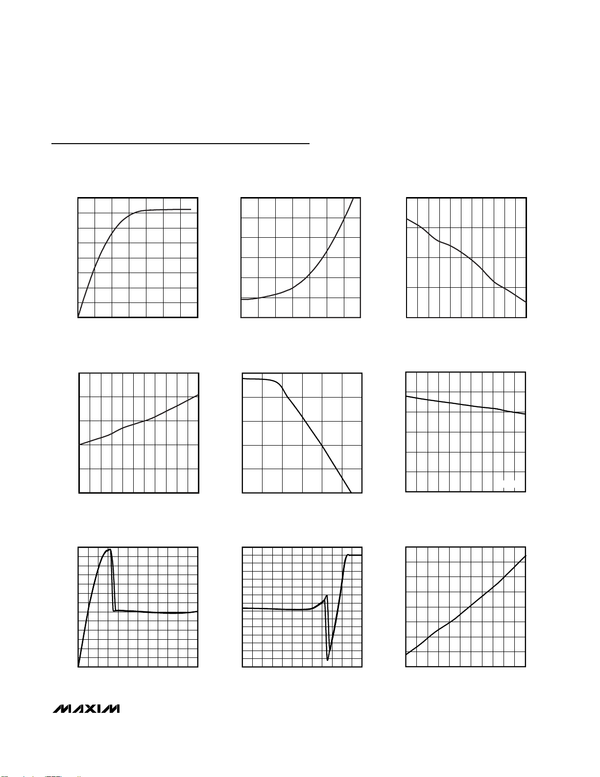
Typical Operating Characteristics
(VCC= +3.3V, TA = +25°C, unless otherwise noted.)
0
10
5
20
15
35
30
25
40
0 1.00.5 1.5 2.0 2.5 3.0 3.5
OUTPUT CURRENT vs. RECEIVER OUTPUT
LOW VOLTAGE
MAX3362 toc01
RECEIVER OUTPUT LOW VOLTAGE (V)
OUTPUT CURRENT (mA)
-30
-20
-25
-10
-15
-5
0
0 1.5 2.00.5 1.0 2.5 3.0 3.5
OUTPUT CURRENT vs. RECEIVER OUTPUT
HIGH VOLTAGE
MAX3362 toc02
RECEIVER OUTPUT HIGH VOLTAGE (V)
OUTPUT CURRENT (mA)
3.22
3.23
3.25
3.24
3.26
-40 -10 5
35
50-25 65 80 95 110 125
RECEIVER OUTPUT HIGH VOLTAGE
vs. TEMPERATURE
MAX3362 toc03
TEMPERATURE (°C)
RECEIVER OUTPUT HIGH VOLTAGE (V)
20
0
0.01
0.02
0.03
0.04
0.05
-40 -10 5-25 20 35 50 65 80 95 110 125
RECEIVER OUTPUT LOW VOLTAGE
vs. TEMPERATURE
MAX3362 toc04
TEMPERATURE (°C)
RECEIVER OUTPUT LOW VOLTAGE (V)
DRIVER OUTPUT CURRENT
vs. DIFFERENTIAL OUTPUT VOLTAGE
MAX3362 toc05
DIFFERENTIAL OUTPUT VOLTAGE (V)
DRIVER OUTPUT CURRENT (mA)
3.23.02.82.62.4
15
30
45
60
75
0
2.2 3.4
DRIVER DIFFERENTIAL OUTPUT VOLTAGE
vs. TEMPERATURE
MAX3362 toc06
TEMPERATURE (°C)
DRIVER DIFFERENTIAL OUTPUT VOLTAGE (V)
1109580655035205-10-25
0.5
1.0
1.5
2.0
2.5
3.0
0
-40 125
RL = 54Ω
DRIVER OUTPUT CURRENT
vs. DRIVER OUTPUT LOW VOLTAGE
MAX3362 toc07
DRIVER OUTPUT LOW VOLTAGE (V)
DRIVER OUTPUT CURRENT (mA)
11108 92 3 4 5 6 71
10
20
30
40
50
60
70
80
90
100
110
120
130
0
012
DRIVER OUTPUT CURRENT
vs. DRIVER OUTPUT HIGH VOLTAGE
MAX3362 toc08
DRIVER OUTPUT HIGH VOLTAGE (V)
DRIVER OUTPUT CURRENT (mA)
431 2-5 -4 -3 -2 -1 0-6
-130
-120
-110
-100
-90
-80
-70
-60
-50
-40
-30
-20
-10
0
10
-140
-7 5
SUPPLY CURRENT vs. TEMPERATURE
MAX3362 toc09
TEMPERATURE (°C)
I
CC
(mA)
11095-25 -10 5 35 50 6520 80
1.69
1.70
1.71
1.72
1.73
1.74
1.75
1.76
1.68
-40 125
Page 6

MAX3362
3.3V, High-Speed, RS-485/RS-422 Transceiver in
SOT Package
6 _______________________________________________________________________________________
Typical Operating Characteristics (continued)
(VCC= +3.3V, TA = +25°C, unless otherwise noted.)
SHUTDOWN SUPPLY CURRENT
vs. TEMPERATURE
1.4
1.2
1.0
0.8
(µA)
SHDN
0.6
I
0.4
0.2
0
-40 125
TEMPERATURE (°C)
MAX3362 toc10
1109580655035205-10-25
UNLOADED DRIVER OUTPUT
WAVEFORM
DRIVER OUTPUT SKEW vs. TEMPERATURE
0.26
0.24
0.22
0.20
0.18
0.16
0.14
0.12
0.10
0.08
DRIVER OUTPUT SKEW (ns)
0.06
0.04
0.02
0
-40 125
TEMPERATURE (°C)
MAX3362 toc11
RECEIVER PROPAGATION DELAY (ns)
1109565 80-10 5 20 35 50-25
LOADED DRIVER OUTPUT
RECEIVER PROPAGATION DELAY
vs. TEMPERATURE
35
33
31
29
27
25
-40 -10 5
20
TEMPERATURE (°C)
WAVEFORM
35
50-25 65 80 95 110 125
MAX3362 toc12
A
B
f
= 16Mbps
DIN
DRIVER PROPAGATION DELAY
DIN
A
B
f
= 16Mbps
DIN
20ns/div
20ns/div
MAX3362 toc15
MAX3362 toc13
3.3V
0
3.3V
0
2V/div
A
B
f
DIN
R
= 54Ω
L
= 16Mbps
20ns/div
RECEIVER PROPAGATION DELAY
A
B
RO
f
DIN
= 16Mbps
20ns/div
MAX3362 toc14
2V
0
MAX3362 toc16
2V/div
2V/div
Page 7

MAX3362
3.3V, High-Speed, RS-485/RS-422 Transceiver in
SOT Package
_______________________________________________________________________________________ 7
Pin Description
Figure 2. Driver Timing Test Circuit
Figure 3. Driver Propagation Delay
Figure 1. Driver DC Test Load
Figure 4. Driver Enable and Disable Times (t
PDSL
, t
PDZL
, t
PDLS
,
t
PDLZ
)
PIN NAME DESCRIPTION
1RO
2 RE
Receiver Output. RO is high if the receiver input differential (A-B) ≥ 200mV and the receiver is enabled
(RE is low). RO is low if the receiver input differential (A-B) ≤ -200mV and the receiver is enabled.
Receiver Output Enable. Driving RE low enables RO. RO is high impedance when RE is high. Drive RE
high and DE low (disable both receiver and driver outputs) to enter low-power shutdown mode.
Driver Output Enable. Driving DE high enables driver outputs. These outputs are high impedance
3DE
when DE is low. Drive RE high and DE low (disable both receiver and driver outputs) to enter lowpower shutdown mode.
4DI
D r i ver Inp ut. D r i vi ng D I l ow for ces the noni nver ti ng outp ut l ow and i nver ti ng outp ut hi g h, w hen the d r i ver i s
enab l ed ( D E i s hi g h) . D r i vi ng D I hi g h for ces the noni nver ti ng outp ut hi g h and i nver ti ng outp ut l ow .
5 GND Ground
6 A Noninverting Receiver Input and Noninverting Driver Output
7 B Inverting Receiver Input and Inverting Driver Output
8VCCSupply Voltage. VCC = 3.3V ±5%. Bypass V
RL/2
D
V
CC
V
OD
R
/2
L
V
OC
to GND with a 0.1µF capacitor.
CC
V
CC
D
R
C
L
C
R
L
L
= 50pF
L
= 54Ω
OUT
t
V
DI
A - B
CC
/2
V
CC
0
B
(A+B)/2
A
90%
10%
ri
t
PDLH
t
DR
V
t
fi
t
PDHL
t
DF
tri = 5ns
= 5ns
t
fi
OUT
S1
0 or 3V
GENERATOR
IN
t
, t
PDSL
PDZL
V
OL
D
50Ω
VOM = (VOL + VCC) /2
CC
C
L
t
PDLZ
RL = 500Ω
OUT
= 50pF
0.25V
V
CC
/2
V
CC
0
V
CC
Page 8

MAX3362
3.3V, High-Speed, RS-485/RS-422 Transceiver in
SOT Package
8 _______________________________________________________________________________________
Figure 5. Driver Enable and Disable Times (t
PDSH
, t
PDZH
, t
PDHS
, t
PDHZ
)
Figure 6. Receiver Propagation Delays
IN
OUT
V
OL
0 or 3V
GENERATOR
, t
t
PDSH
PDZH
GENERATOR
V
D
50Ω
= (VOH) /2
OM
50Ω
V
S1
C
L
ID
= 50pF
R
OUT
RL = 500Ω
V
CC
/2
V
CC
0
0.25V
V
t
PDHZ
CC
OUT
CL = 15pF
V
CC
t
PRHL
VOM =
2
3.0V
0
V
CC
V
OM
0
IN
OUT
1.5V
0
1.5V 1.5V
t
PRLH
V
OM
V
OL
Page 9
MAX3362
3.3V, High-Speed, RS-485/RS-422 Transceiver in
SOT Package
_______________________________________________________________________________________ 9
Detailed Description
The MAX3362 low-power, high-speed transceiver for
RS-485/RS-422 communication operates from a single
+3.3V power supply. The device contains one differential line driver and one differential line receiver. The driver and receiver may be independently enabled. When
disabled, outputs enter a high-impedance state.
The transceiver guarantees data rates up to 20Mbps,
with an output skew of less than 6ns. This low skew
time makes the MAX3362 ideal for multidrop clock/data
distribution applications, such as cellular base stations.
Driver and receiver propagation delays are below 50ns.
The output level is guaranteed at 1.5V on a standard
54Ω load.
The device has a hot-swap feature that eliminates false
transitions on the data cable during circuit initialization.
Also, drivers are short-circuit current limited and are
protected against excessive power dissipation by thermal shutdown circuitry.
Figure 7. Receiver Enable and Disable Times
OUT
IN
IN
OUT
0.25V
1.5V
t
PRHZ
1.5V
-1.5V
S1 OPEN
S2 CLOSED
S3 = 1.5V
S1 OPEN
S2 CLOSED
S3 = 1.5V
S3
GENERATOR
1.5V
t
PRZH
t
PRSH
1.5V
S1
S2
0.25V
t
PRLZ
V
CC
S1 CLOSED
S2 OPEN
S3 = -1.5V
S1 CLOSED
S2 OPEN
S3 = -1.5V
1.5V
t
t
PRZL
PRSL
1.5V
3V
0
V
OC
V
OL
3V
0
V
OH
0
R
= 1kΩ
V
R
ID
50Ω
3V
0
V
OH
0
3V
0
V
OH
0
L
C
L
IN
OUT
IN
OUT
Page 10

MAX3362
3.3V, High-Speed, RS-485/RS-422 Transceiver in
SOT Package
10 ______________________________________________________________________________________
The MAX3362 has a 1/8-unit-load receiver input impedance, allowing up to 256 transceivers to be connected
simultaneously on a bus. The MAX3362 is designed for
half-duplex communication.
Driver
The driver transfers single-ended input (DI) to differential outputs (A, B). The driver enable (DE) input controls
the driver. When DE is high, driver outputs are enabled.
These outputs are high impedance when DE is low.
When the driver is enabled, setting DI low forces the
noninverting output (A) low and inverting output (B)
high. Conversely, drive DI high to force noninverting
output high and inverting output low (Table 1).
Drive RE high and DE low (disable both receiver and
driver outputs) to enter low-power shutdown mode.
Receiver
The receiver reads differential inputs from the bus lines
(A, B) and transfers this data as a single-ended output
(RO). The receiver enable (RE) input controls the
receiver. Drive RE low to enable the receiver. Driving
RE high places RO into a high-impedance state.
When the receiver is enabled, RO is high if (A-B) ≥
200mV. RO is low if (A-B) ≤ -200mV.
Drive RE high and DE low (disable both receiver and
driver outputs) to enter low-power shutdown mode.
Hot-Swap Capability
Hot-Swap Input
When circuit boards are inserted into a hot or powered
backplane, disturbances to the enable and differential
receiver inputs can lead to data errors. Upon initial circuit board insertion, the processor undergoes its
power-up sequence. During this period, the output drivers are high impedance and are unable to drive the
DE input of the MAX3362 to a defined logic level.
Leakage currents up to 10µA from the high-impedance
output could cause DE to drift to an incorrect logic
state. Additionally, parasitic circuit board capacitance
could cause coupling of V
CC
or GND to DE. These fac-
tors could improperly enable the driver.
When VCCrises, an internal pulldown circuit holds DE
low for at least 10µs and until the current into DE
exceeds 200µA. After the initial power-up sequence,
the pulldown circuit becomes transparent, resetting the
hot-swap tolerable input.
Hot-Swap Input Circuitry
The MAX3362 enable inputs feature hot-swap capability.
At the input there are two NMOS devices, M1 and M2
(Figure 8). When VCCramps from 0, an internal 10µs
timer turns on M2 and sets the SR latch, which also turns
on M1. Transistors M2, a 300µA current sink, and M1, a
30µA current sink, pull DE to GND through an 8kΩ resistor. M2 is designed to pull DE to the disabled state
against an external parasitic capacitance up to 100pF
that may drive DE high. After 10µs, the timer deactivates
M2 while M1 remains on, holding DE low against threestate leakages that may drive DE high. M1 remains on
until an external source overcomes the required input
current. At this time, the SR latch resets and M1 turns off.
When M1 turns off, DE reverts to a standard, highimpedance CMOS input. Whenever VCCdrops below
1V, the hot-swap input is reset.
For RE there is a complimentary circuit employing two
PMOS devices pulling RE to VCC.
Hot-Swap Line Transient
The circuit of Figure 9 shows a typical offset termination
used to guarantee a greater than 200mV offset when a
line is not driven (the 50pF represents the minimum
parasitic capacitance that would exist in a typical application). During a hot-swap event when the driver is
Table 1. Transmitter Functional Table
Table 2. Receiver Functional Table
INPUTS OUTPUTS
RE DE DI A B
X11 1 0
X10 0 1
0 0 X High Z High Z
1 0 X Shutdown
RE DE A – BRO
0X≥ 200mV 1
0X≤ -200mV 0
1 1 X High-Z
1 0 X Shutdown
TRANSMITTING
RECEIVING
INPUTS OUTPUT
Page 11

MAX3362
3.3V, High-Speed, RS-485/RS-422 Transceiver in
SOT Package
______________________________________________________________________________________ 11
Figure 8. Simplified Structure of the Driver Enable Input (DE)
Figure 9. Differential Power-Up Glitch (Hot Swap)
Figure 10. Differential Power-Up Glitch (0.1V/µs)
V
CC
10µs
TIMER
TIMER
DE
8kΩ
30µA
M1 M2
3.3V
1kΩ
0.1kΩ
1kΩ
50pF
V
CC
T
OR GND
V
CC
Y
IN
Z
300µA
V
A-B
DE
(HOT SWAP)
3.3V
CC
A
B
0
10mV/div
AC-COUPLED
10mV/div
AC-COUPLED
10mV/div
10µs/div
Page 12

MAX3362
3.3V, High-Speed, RS-485/RS-422 Transceiver in
SOT Package
12 ______________________________________________________________________________________
connected to the line and is powered up the driver
must not cause the differential signal to drop below
200mV. Figures 10, 11, and 12 show the results of the
MAX3362 during power-up for three different VCCramp
rates (0.1V/µs, 1V/µs, and 10V/µs). The photos show
the VCCramp, the single-ended signal on each side of
the 100Ω termination, as well as the differential signal
across the termination.
Low-Power Shutdown Mode
Low-power shutdown mode is initiated by bringing both
RE high and DE low. In shutdown, the MAX3362 typically draws only 1µA supply current.
RE and DE may be driven simultaneously; the device is
guaranteed not to enter shutdown if RE is high and DE
is low for less than 50ns. If the inputs are in this state
for at least 600ns, the device will enter shutdown.
Enable times t
PDZH, tPDZL, tPRZH
and t
PRZL
in the
Switching Characteristics table assume the device was
not in a low-power shutdown state. Enable times t
PDSH,
t
PDSL, tPRSH,
and t
PRSL
assume the device was shut
down. Drivers and receivers take longer to become
enabled from low-power shutdown mode than from
driver/receiver disable mode.
Applications Information
Propagation Delays
Figures 5 and 6 show the typical propagation delays.
Skew time is simply the difference between the low-tohigh and high-to-low propagation delay. Small
driver/receiver skew times help maintain a symmetrical
mark-space ratio (50% duty cycle). Both the receiver
skew time and driver skew time are under 6ns.
256 Transceivers on the Bus
The standard RS-485 receiver input impedance is 12kΩ
(one-unit load), and a standard driver can drive up to
32 unit loads. The MAX3362 transceiver has a 1/8-unitload receiver input impedance (96kΩ), allowing up to
256 transceivers to be connected in parallel on one
communication line. Any combination of these devices
and/or other RS-485 transceivers with a total of 32 unit
loads or less can be connected to the line.
Driver Output Protection
Two mechanisms prevent excessive output current and
power dissipation caused by faults or by bus contention. The first, a foldback current limit on the output
stage, provides immediate protection against short circuits over the whole common-mode voltage range (see
Typical Operating Characteristics). The second, a thermal shutdown circuit, forces the driver outputs into a
high-impedance state if the die temperature becomes
excessive.
Typical Applications
The MAX3362 transceiver is designed for bidirectional
data communications on multipoint bus transmission
lines. The Typical Operating Circuit shows a typical network applications circuit. To minimize reflections, the
line should be terminated at both ends in its characteristic impedance, and stub lengths off the main line
should be kept as short as possible.
Figure 11. Differential Power-Up Glitch (1V/µs)
Figure 12. Differential Power-Up Glitch (10V/µs)
3.3V
V
CC
A
B
A-B
1µs/div
0
10mV/div
AC-COUPLED
10mV/div
AC-COUPLED
10mV/div
3.3V
V
CC
A
B
A-B
200ns/div
0
50mV/div
AC-COUPLED
50mV/div
AC-COUPLED
10mV/div
Page 13

MAX3362
3.3V, High-Speed, RS-485/RS-422 Transceiver in
SOT Package
______________________________________________________________________________________ 13
Pin Configuration
RD
DI
V
CC
RE
B
A
GND
DE
R
D
MAX3362
Functional Diagram
Chip Information
TRANSISTOR COUNT: 708
PROCESS: BiCMOS
TOP VIEW
1
RO
2
MAX3362
3
DE
4
SOT23
87V
6
5
CC
BRE
A
GNDDI
Page 14

MAX3362
3.3V, High-Speed, RS-485/RS-422 Transceiver in
SOT Package
Maxim cannot assume responsibility for use of any circuitry other than circuitry entirely embodied in a Maxim product. No circuit patent licenses are
implied. Maxim reserves the right to change the circuitry and specifications without notice at any time.
14 ____________________Maxim Integrated Products, 120 San Gabriel Drive, Sunnyvale, CA 94086 408-737-7600
© 2002 Maxim Integrated Products Printed USA is a registered trademark of Maxim Integrated Products.
Package Information
(The package drawing(s) in this data sheet may not reflect the most current specifications. For the latest package outline information,
go to www.maxim-ic.com/packages.)
SOT23, 8L.EPS
 Loading...