

Page 1
现货库存、技术资料、百科信息、热点资讯,精彩尽在鼎好!
General Description
The MAX3355E integrates a charge pump and comparators to enable a system with an integrated USB onthe-go (OTG) dual-role transceiver to function as a USB
OTG dual-role device. USB OTG facilitates the direct
connection of peripherals and mobile devices such as
PDAs, cellular phones, MP3 players, and digital cameras to one another without a host PC.
The MAX3355E’s internal charge pump supplies V
BUS
power and signaling that is required by the transceiver as
defined in On-the-Go Supplement to the USB 2.0
Specification, Revision 1.0. The MAX3355E features ID
detection and internal comparators for monitoring
V
BUS
. The V
BUS
status outputs are used during negotiation for the USB according to the session request protocol (SRP) and host negotiation protocol (HNP).
The MAX3355E operates with logic supply voltages
(VL) as low as 1.65V, ensuring compatibility with lowvoltage ASICs. The device also features a logic-selectable 1µA shutdown mode.
The MAX3355E has built-in ±15kV ESD-protection circuitry to protect the V
BUS
and ID_IN pins. The device is
available in a miniature 4 x 3 chip-scale package
(UCSP), as well as a 14-pin TSSOP package, and is
specified for operation over the -40°C to +85°C extended
temperature range.
Applications
Cell Phones MP3 Players
PDAs Digital Cameras
Features
♦ Guaranteed 8mA (min) V
BUS
Charge-Pump Output
♦ ±15kV ESD Protection on V
BUS
and ID_IN
♦ Up to +6.0V Backdrive Capability for V
BUS
♦ +2.6V to +5.5V Operating Voltage Range
♦ V
L
Operates Down to +1.65V
♦ Guaranteed V
BUS
Input Impedance When Not
Driven
♦ Automatic C
LOAD
Detection
♦ Comparators for Host Negotiation Protocol
♦ ID_IN Detection
♦ Available in 4 x 3 UCSP or 14-Pin TSSOP Package
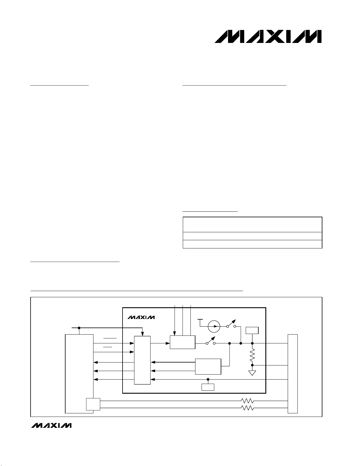
MAX3355E
±15kV ESD-Protected USB On-the-Go
Charge Pump and Comparators in UCSP
________________________________________________________________ Maxim Integrated Products 1
Ordering Information
CHARGE
PUMP
5V AT 8mA
40kΩ TO
100kΩ
STATUS2
STATUS1
ON/OFF
MAX3355E
V
BUS
COMPARATORS
CURRENT
SOURCE
V
BUS
V
BUS
GND
USB CONNECTOR
ID_IN
GND
ID
D+
D-
V
CC
V
L
C+
V
CC
C-
ESD
LEVEL
SHIFTER
OFFVBUS
SHDN
STATUS1
STATUS2
ID_OUT
DUAL-ROLE
ASIC
LOGIC SUPPLY
+1.65V TO V
CC
USB
XCVR
ESD
Functional Diagram
19-2844; Rev 1; 8/03
For pricing, delivery, and ordering information, please contact Maxim/Dallas Direct! at
1-888-629-4642, or visit Maxim’s website at www.maxim-ic.com.
Pin Configurations appear at end of data sheet.
PART TEMP RANGE
MAX3355EEBC-T -40°C to +85°C 4 x 3 UCSP ABE
MAX3355EEUD -40°C to +85°C 14 TSSOP —
PINPACKAGE
TOP
MARK
Page 2
MAX3355E
±15kV ESD-Protected USB On-the-Go
Charge Pump and Comparators in UCSP
2 _______________________________________________________________________________________
ABSOLUTE MAXIMUM RATINGS
ELECTRICAL CHARACTERISTICS
(VCC= +2.6V to +5.5V, VL= +1.65V to VCC, C1 = 0.1µF, VCCdecoupled with 1µF capacitor to GND, VLdecoupled with 0.1µF
capacitor to GND, C
LOAD
= 1µF (min), ESR
LOAD
= 1Ω (max), TA= T
MIN
to T
MAX
. Typical values are at VCC= +3.0V, VL= 1.8V, TA=
+25°C, unless otherwise noted.) (Notes 1, 2)
Stresses beyond those listed under “Absolute Maximum Ratings” may cause permanent damage to the device. These are stress ratings only, and functional
operation of the device at these or any other conditions beyond those indicated in the operational sections of the specifications is not implied. Exposure to
absolute maximum rating conditions for extended periods may affect device reliability.
(All voltages referenced to GND)
V
CC
, VL, V
BUS
, ID_IN.............................................-0.3V to +6.0V
C+..................................................................(V
CC
- 0.3V) to +6V
C-................................................................-0.3V to (V
CC
+ 0.3V)
OFFVBUS, SHDN, STATUS1,
STATUS2, ID_OUT ....................................-0.3V to (V
L
+ 0.3V)
V
BUS
Short Circuit to GND .........................................Continuous
Output Current (all other pins)..........................................±15mA
Continuous Power Dissipation (T
A
= +70°C)
4 x 3 UCSP (derate 6.5mW/°C above +70°C) .............520mW
14-Pin TSSOP (derate 9.1mW/°C above +70°C) .........727mW
Operating Temperature Range ...........................-40°C to +85°C
Storage Temperature Range .............................-65°C to +150°C
Junction Temperature......................................................+150°C
Lead Temperature (soldering, 10s) .................................+300°C
Bump Temperature (soldering)
Infrared (15s) ...............................................................+200°C
Vapor Phase (20s) .......................................................+215°C
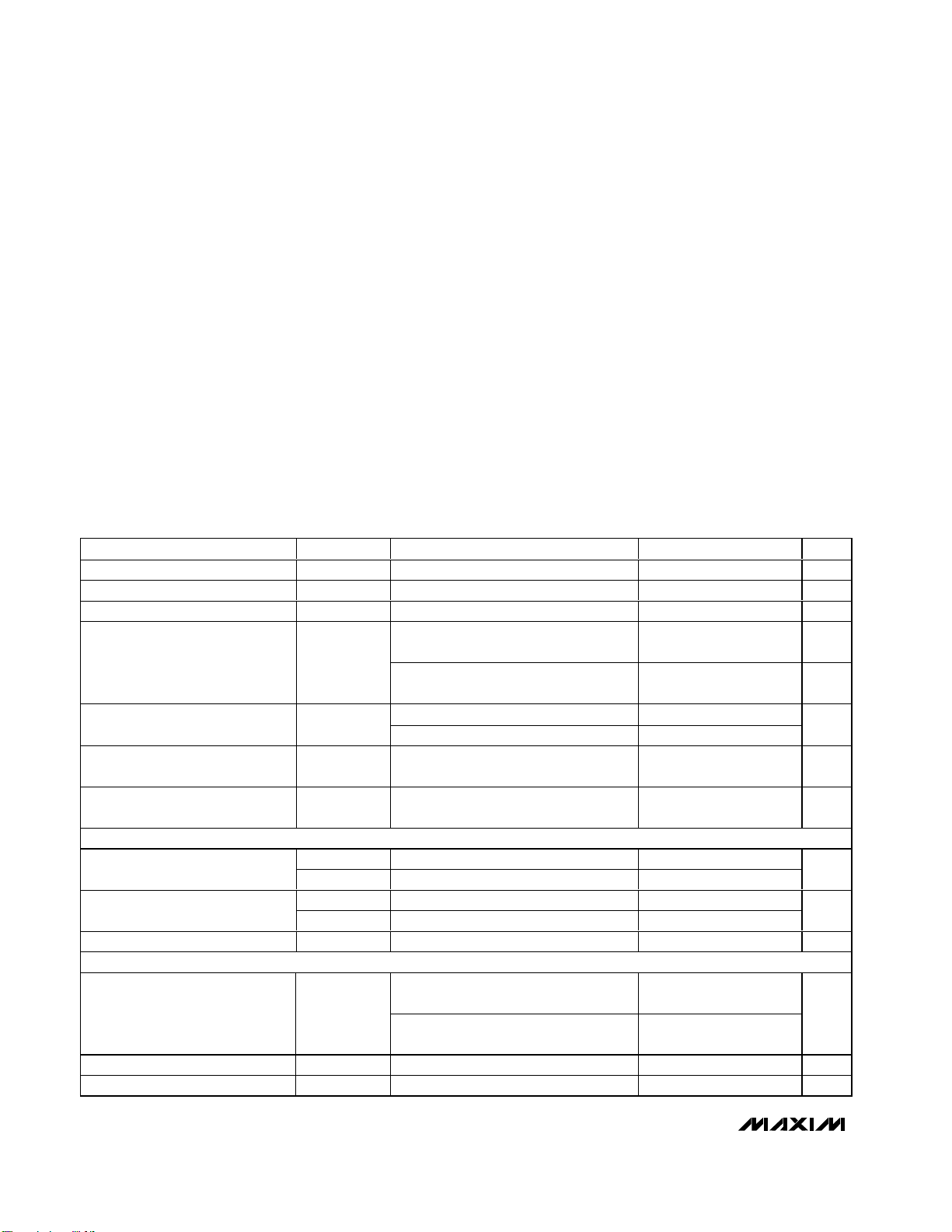
PARAMETER SYMBOL CONDITIONS MIN TYP MAX UNITS
Supply Voltage V
Logic Supply Voltage V
Logic Supply Current I
Operating Supply Current I
Shutdown Supply Current I
Thermal-Shutdown Protection
Threshold
Thermal-Shutdown Protection
Hysteresis
LOGIC INPUTS AND OUTPUTS
STATUS1, STATUS2, ID_OUT
Output Voltage
OFFVBUS, SHDN Input Voltage
Input Leakage Current I
V
OUTPUT VOLTAGE: DEVICE A CONFIGURED
BUS
V
Output Voltage
BUS
V
Leakage Voltage OFFVBUS = GND 200 mV
BUS
V
Sink Current OFFVBUS = GND, V
BUS
CC
L
L
CC
CCSHDN
V
OH
V
OL
V
IH
V
IL
LKG
No activity on V
reference active
Device A configured, OFFVBUS = VL,
I
= 8mA, charge pump on
LOAD
Device B configured, SHDN = GND 1
Device A configured, SHDN = GND 30
Device A configured, OFFVBUS = VL,
charge pump on
Device A configured, OFFVBUS = VL,
charge pump on
I
SOURCE
I
SINK
= +1mA 2/3 x V
= -1mA 0.4
OFFVBUS, SHDN = GND or V
I
= 0 to 8mA, C
LOAD
OFFVBUS = V
No load, C
ID_IN = GND
2.6 5.5 V
1.65 V
CC
100 µA
; comparator and
BUS
200 µA
20 mA
+150 °C
+20 °C
L
2/3 x V
L
0.4
±1 µA
= 1µF,
LOAD
, ID_IN = GND
L
= 1µF, OFFVBUS = VL,
LOAD
= +6.0V 150 µA
BUS
L
4.63 5.25
4.8
V
µA
V
V
V
Page 3
MAX3355E
±15kV ESD-Protected USB On-the-Go
Charge Pump and Comparators in UCSP
_______________________________________________________________________________________ 3
ELECTRICAL CHARACTERISTICS (continued)
(VCC= +2.6V to +5.5V, VL= +1.65V to VCC, C1 = 0.1µF, VCCdecoupled with 1µF capacitor to GND, VLdecoupled with 0.1µF
capacitor to GND, C
LOAD
= 1µF (min), ESR
LOAD
= 1Ω (max), TA= T
MIN
to T
MAX
. Typical values are at VCC= +3.0V, VL= 1.8V, TA=
+25°C, unless otherwise noted.) (Notes 1, 2)
V
BUS
V
BUS
V
BUS
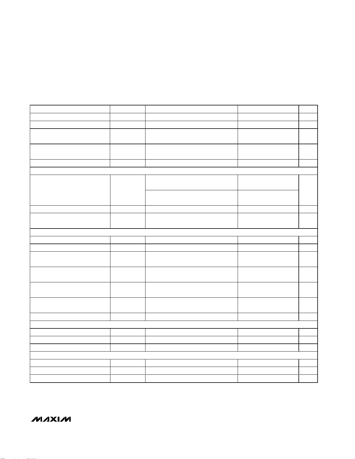
PARAMETER SYMBOL CONDITIONS MIN TYP MAX UNITS
Source Current OFFVBUS = V
Short-Circuit Current Limit V
Output Ripple
Charge-Pump Switching
Frequency
V
Input Impedance R
BUS
LOAD DETECTION V
V
Output Voltage
BUS
V
Source Current OFFVBUS = VL, ID_IN = VCC (Note 4) 450 600 850 µA
BUS
V
Current Gate Time t
BUS
V
COMPARATOR
BUS
V
Valid Comparator Threshold V
BUS
V
Valid Comparator Hysteresis 20 mV
BUS
Session Valid Comparator
Threshold
Session Valid Comparator
Hysteresis
B-Session End Comparator
Threshold
B-Session End Comparator
Hysteresis
Shutdown Comparator V
ID_IN
ID_IN Voltage Input for Device B 2/3 x V
ID_IN Voltage Input for Device A 0.4 V
ID_IN Input Impedance 150 200 250 kΩ
ESD PROTECTION (ID_IN, V
Human Body Model ±15 kV
IFC 1000-4-2 Air-Gap Discharge ±15 kV
IFC 1000-4-2 Contact Discharge ±8 kV
OUTPUT VOLTAGE
BUS
BUS
INVBUS
VBUSCHRG
THVBUSVLDVBUS
V
THSESVLD
V
THSESEND
TH,SHDN
)
shorted to GND 200 mA
BUS
I
= 8mA, C
LOAD
OFFVBUS = V
ID_IN = GND 8 mA
L,
LOAD
, ID_IN = GND (Note 3)
L
= 1µF,
100 mV
500 kHz
OFFVBUS = GND or SHDN = GND 40 100 kΩ
C
= 20µF, OFFVBUS = VL, ID_IN =
LOAD
V
, I
source on-time = t
BUS
VBUSCHRG
= 95µF, OFFVBUS = VL, ID_IN =
, I
source on-time = t
BUS
VBUSCHRG
C
V
CC
LOAD
CC
OFFVBUS = VL, ID_IN = VCC, Device B
(Note 4)
2.1
155
(max)
105
1.9
(min)
rising 4.4 4.55 4.63 V
1.12 1.4 1.68 V
15 mV
0.4 0.5 0.6 V
30 mV
0.8 2.4 V
cc
56
V
ms
V
Page 4
MAX3355E
±15kV ESD-Protected USB On-the-Go
Charge Pump and Comparators in UCSP
4 _______________________________________________________________________________________
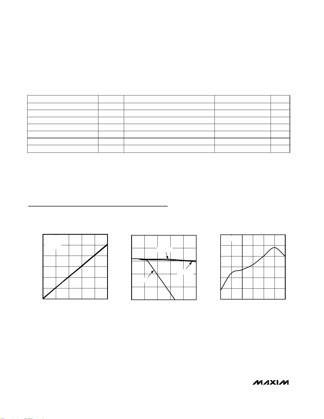
Typical Operating Characteristics
(VCC, VL= +3.3V, C1 = 0.1µF, VCCdecoupled with 1µF capacitor to GND, VLdecoupled with 0.1µF capacitor to GND, C
LOAD
= 1µF
min, ESR
LOAD
= 1Ω max, TA= +25°C, unless otherwise noted.)
0
40
20
80
60
100
120
050
VCC INPUT CURRENT
vs. V
BUS
OUTPUT CURRENT
MAX3355E toc01
V
BUS
OUTPUT CURRENT (mA)
V
CC
INPUT CURRENT (mA)
2010 30 40
VCC = 2.6V
V
CC
= 4.0V
V
CC
= 5.5V
4.00
4.50
4.25
4.75
5.00
5.25
050
V
BUS
OUTPUT VOLTAGE
vs. V
BUS
OUTPUT CURRENT
MAX3355E toc02
V
BUS
OUTPUT CURRENT (mA)
V
BUS
OUTPUT VOLTAGE (V)
2010 30 40
VCC = 4.0V
VCC = 5.5V
VCC = 2.6V
0
75
25
50
100
125
150
2.5 5.5
V
BUS
OUTPUT RIPPLE VOLTAGE
vs. V
CC
INPUT VOLTAGE
MAX3355E toc03
V
CC
INPUT VOLTAGE (V)
V
BUS
OUTPUT RIPPLE VOLTAGE (mV)
3.53.0 4.0 5.04.5
I
VBUS
= 8mA
TIMING CHARACTERISTICS
(VCC= +2.6V to +5.5V, VL= +1.65V to VCC, C1 = 0.1µF, VCCdecoupled with 1µF capacitor to GND, VLdecoupled with 0.1µF
capacitor to GND, C
LOAD
= 1µF (min), ESR
LOAD
= 1Ω (max), TA= T
MIN
to T
MAX
. Typical values are at VCC= +3.0V, VL= 1.8V, TA=
+25°C, unless otherwise noted.) (Notes 1, 2)
Note 1: Limits are 100% production tested at +25°C. Limits over temperature are guaranteed by design.
Note 2: All currents out of the device are positive; all currents into the device are negative. All voltages are referenced to device
ground unless otherwise specified.
Note 3: The ripple voltage is strongly correlated to the bus capacitance and its ESR.
Note 4: The V
BUS
current source and current gate time vary together with process and temperature such that the resulting V
BUS
pulse is guaranteed to drive a <13µF load to a voltage >2.0V, and to drive a >96µF load to a voltage <2.2V.
V
BUS
PARAMETER SYMBOL CONDITIONS MIN TYP MAX UNITS
Rise Time 0 to 4.4V, C
OFFVBUS Propagation Delay 6µs
Comparator Propagation Delay 3µs
Time to Exit Shutdown 50 µs
Time to Shutdown 1µs
ID_OUT Rise Time C
ID_OUT Fall Time C
ID_OUT
ID_OUT
= 8mA 100 ms
LOAD
LOAD
= 1µF, I
= 50pF 10 ns
= 50pF 10 ns
Page 5

MAX3355E
±15kV ESD-Protected USB On-the-Go
Charge Pump and Comparators in UCSP
_______________________________________________________________________________________ 5
Typical Operating Characteristics (continued)
(VCC, VL= +3.3V, C1 = 0.1µF, VCCdecoupled with 1µF capacitor to GND, VLdecoupled with 0.1µF capacitor to GND, C
LOAD
= 1µF
min, ESR
LOAD
= 1Ω max, TA= +25°C, unless otherwise noted.)
4.0
4.8
4.2
4.4
4.6
5.0
5.2
5.4
2.5 5.5
V
BUS
OUTPUT VOLTAGE
vs. V
CC
INPUT VOLTAGE
MAX3355E toc04
VCC INPUT VOLTAGE (V)
V
BUS
OUTPUT VOLTAGE (V)
3.53.0 4.0 5.04.5
I
VBUS
= 0mA
I
VBUS
= 8mA
65
67
66
68
69
70
-40 85
V
BUS
INPUT IMPEDANCE
vs. TEMPERATURE
MAX3355E toc05
TEMPERATURE (°C)
V
BUS
INPUT IMPEDANCE (kΩ)
10-15 35 60
16
17
18
19
20
-40 85
SUPPLY CURRENT
vs. TEMPERATURE
MAX3355E toc06
TEMPERATURE (°C)
SUPPLY CURRENT (mA)
10-15 35 60
I
VBUS
= 8mA
VCC = 4.0V
VCC = 2.6V
VCC = 5.5V
V
BUS
vs. CAPACITANCE LOAD
DURING LOAD DETECTION
MAX3355E toc07
C
VBUS
= 10µF
1V/div
C
VBUS
= 96µF
1V/div
40ms/div
0
0
Page 6
MAX3355E
±15kV ESD-Protected USB On-the-Go
Charge Pump and Comparators in UCSP
6 _______________________________________________________________________________________
Typical Application Circuit
Pin Description
PIN
UCSP TSSOP
A1 2 V
A2 3 ID_OUT Device ID Output. Output of ID_IN level translated to VL.
A3 5 STATUS1
A4 6 STATUS2
B1 1 V
B2 4 OFFVBUS V
B3 11 SHDN
B4 9 V
C1 14 C+ Charge-Pump Positive Connection
C2 13 C- Charge-Pump Negative Connection
C3 12 GND Ground
C4 10 ID_IN
— 7, 8 N.C. No Connection
NAME FUNCTION
CC
Power Supply. +2.6V to +5.5V input supply. Bypass VCC to GND with a 1µF capacitor.
Status Output 1. Provides output voltage detection for use during HNP handshaking (Tables 1
and 2).
Status Output 2. Provides output voltage detection for use during HNP handshaking (Tables 1
and 2).
BUS
U S B S up p l y. V
V
i s l ow er than + 2.1V w hen ID _IN i s op en or a l oad g r eater than 96.5µF i s sensed . V
B U S
p r ovi d es a nom i nal + 5.0V outp ut w hen ID _IN i s l ow and O FFVBUS i s hi g h.
B U S
b e b ackd r i ven to + 6.0V w i thout any conseq uence. Byp ass V
Off. Turns the internal charge pump providing V
BUS
Shutdown. Connect SHDN to GND to enter shutdown and reduce supply current to less than
1µA. Connect SHDN to V
Logic Supply. VL sets the logic output high voltage and logic input high threshold. VL must be
L
between +1.65V and V
Device ID. ID_IN is internally pulled up to V
for normal operation.
L
.
CC
Leave ID_IN open for device B and connect
CC.
ID_IN to GND for device A.
B U S
on and off.
BUS
can
to G N D w i th a 1µF cap aci tor .
B U S
V
CC
V
1µF
L
0.1µF
V
CC
V
L
MAX3355E
OFFVBUS
ID_OUT
STAT US1
µP
OTG SIE
D+
D-
STAT US2
SHDN
V
BUS
ID_IN
GND
C+
C1
0.1µF
C-
C
LOAD
1µF
USB OTG
CONNECTOR
Page 7
Detailed Description
USB OTG is an emerging USB standard that enables
devices to talk in a peer-to-peer manner on a USB bus.
OTG allows peripherals and mobile devices such as
PDAs, cellular phones, and digital cameras to be
attached directly to one another without requiring a
PC host.
The MAX3355E integrates a charge pump and comparators to enable a system with an integrated USB OTG
dual-role transceiver to function as a USB OTG dual-role
device. The MAX3355E’s internal charge pump supplies
V
BUS
power and signaling as defined in On-the-Go
Supplement: USB 2.0, Revision 1.0. The MAX3355E’s
internal level-detection comparators monitor important
V
BUS
voltages needed to support SRP and HNP.
Charge Pump
The MAX3355E provides power for the V
BUS
line using
an internal charge pump. The charge pump provides
an OTG-compliant output on V
BUS
while sourcing 8mA
load current. The charge pump can be powered from
voltages between +2.6V and +5.5V. A 0.1µF flying
capacitor, connected between C+ and C-, and a 1µF
(min) decoupling reservoir capacitor on V
BUS
are
required for proper operation.
The charge pump is active if OFFVBUS is connected to
VLand the MAX3355E is configured as device A (ID_IN
connected to GND). To minimize V
BUS
ripple, select a
reservoir capacitor value between 1µF and 6.8µF. The
charge-pump output is protected from short-circuit conditions on V
BUS
by an internal current clamp that limits
the V
BUS
current to 200mA.
Current Generator
An internal current generator injects up to 600µA of current onto the V
BUS
line. The current generator is stable
over the supply voltage variation. The current generator
is connected to V
BUS
when OFFVBUS and SHDN are 1
and ID_IN is open. It remains connected for t
VBUSCHRG
or until the V
BUS
line voltage exceeds the lower of V
CC
and 4.82V.
Comparators
The MAX3355E contains internal comparators for monitoring the V
BUS
voltage. The status of V
BUS
is summarized in two status outputs: STATUS1 and STATUS2.
The status outputs can be used to negotiate for the
USB OTG bus. The V
BUS
status is conveyed according
to Table 1. While in shutdown mode, the STATUS2 output can be used to indicate V
BUS
voltage (Table 2).
Device ID
Configure the MAX3355E as device A by connecting
ID_IN to GND and as device B by leaving ID_IN open
(Table 3). ID_IN is level translated to VLand provided
as an output at ID_OUT. VL sets the logic output high
level. ID_IN is internally pulled up to VCC.
MAX3355E
±15kV ESD-Protected USB On-the-Go
Charge Pump and Comparators in UCSP
_______________________________________________________________________________________ 7
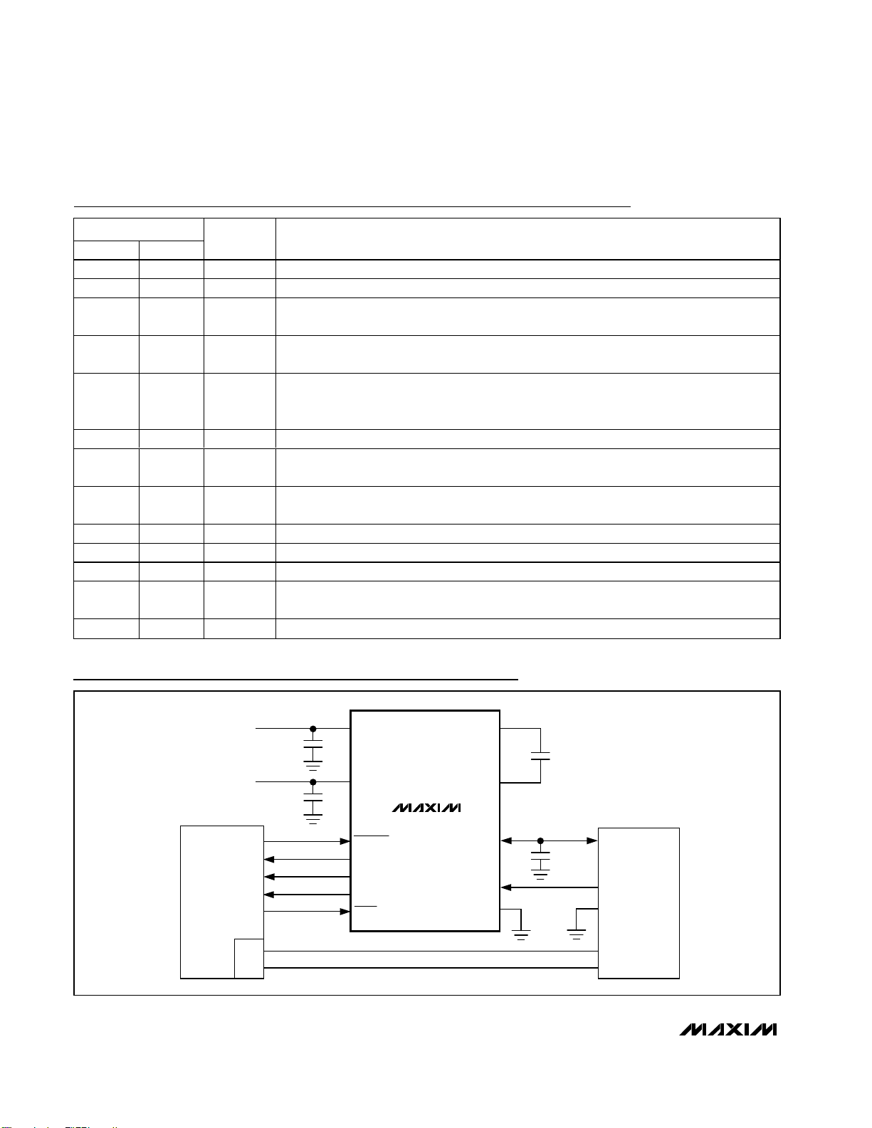
Table 1. Status Bit Significance
Table 2. Status Bit Shutdown
Functionality (SHDN = GND)
Table 3. Device ID
Table 4. Function Select
Note: The 600µA current source is supplied for t
VBUSCHRG
(see the Current Generator section).
STATUS1 STATUS2 SIGNIFICANCE
00 V
10V
01V
11 V
THSESEND
THSESVLD
BUS
BUS
< V
< V
< V
> V
THSESEND
< V
BUS
< V
BUS
THVBUSVLD
THVBUSVLD
THSESVLD
STATUS1 STATUS2 SIGNIFICANCE
01 V
00 V
ID_IN ID_OUT CONFIGURATION
0 0 Device A
Open V
L
BUS
BUS
< V
TH,SHDN
> V
TH,SHDN
Device B
SHDN OFFVBUS ID_IN V
0XXR
10XR
1 1 0 5V Active Active
111R
BUS
INVBUS
INVBUS
(Note 5) Inactive Active
INVBUS
CHARGE PUMP COMPARATORS
Inactive Inactive
Inactive Active
Page 8

MAX3355E
OFFVBUS
Connect OFFVBUS to GND to disable V
BUS
and the
charge pump (Table 4). For normal V
BUS
operation,
connect OFFVBUS to VL. When OFFVBUS = GND, V
BUS
impedance is between 40kΩ to 100kΩ as defined in On-
the-Go Supplement: USB 2.0, Revision 1.0.
SHDN
The MAX3355E shutdown mode reduces supply current
to less than 1µA. To enter shutdown mode, connect
SHDN to GND. Shutdown mode disables the charge
pump and comparators (Table 4). While in shutdown
mode, the STATUS1 output defaults to logic 0 and STATUS2 indicates V
BUS
. During shutdown, if V
BUS
is exter-
nally driven above V
TH,SHDN
(defined in the Comparators
section), the MAX3355E sinks current from VCC.
Applications Information
±15kV ESD Protection
To protect the MAX3355E against ESD, ID_IN and V
BUS
have extra protection against static electricity to protect
the device up to ±15kV. For ±15kV protection on V
BUS
,
a 1µF capacitor must be connected from V
BUS
to GND
as close to the device as possible. The ESD structures
withstand high ESD in all states—normal operation,
shutdown, and powered down. ESD protection can be
tested in various ways. The ID_IN input and V
BUS
are
characterized for protection to the following limits:
1) ±15kV using the Human Body Model
2) ±8kV using the IEC 1000-4-2 Contact Discharge
method
3) ±15kV using the IEC 1000-4-2 Air-Gap Discharge
method
ESD performance depends on a variety of conditions.
Contact Maxim for a reliability report that documents
test setup, test methodology, and test results.
Human Body Model
Figure 1 shows the Human Body Model and Figure 2
shows the current waveform it generates when discharged into a low impedance. This model consists of a
100pF capacitor charged to the ESD voltage of interest,
which is then discharged into the test device through a
1.5kΩ resistor.
IEC 1000-4-2
The IEC 1000-4-2 standard covers ESD testing and
performance of finished equipment. It does not specifically refer to integrated circuits. The MAX3355E helps
the user design equipment that meets Level 4 of IEC
1000-4-2, without the need for additional ESD-protection components. The major difference between tests
done using the Human Body Model and IEC 1000-4-2
is a higher peak current in IEC 1000-4-2. This occurs
because series resistance is lower in the IEC 1000-4-2
model. Hence, the ESD withstand voltage measured to
±15kV ESD-Protected USB On-the-Go
Charge Pump and Comparators in UCSP
8 _______________________________________________________________________________________
Figure 1. Human Body ESD Test Model
Figure 2. Human Body Current Waveform
Figure 3. IEC 1000-4-2 ESD Test Model
R
D
1.5kΩ
DISCHARGE
RESISTANCE
STORAGE
CAPACITOR
HIGH-
VOLTAGE
DC
SOURCE
R
C
1MΩ
CHARGE-CURRENT-
LIMIT RESISTOR
C
100pF
s
IP 100%
90%
AMPERES
36.8%
10%
0
0
t
RL
TIME
t
DL
CURRENT WAVEFORM
PEAK-TO-PEAK RINGING
I
r
(NOT DRAWN TO SCALE)
DEVICE
UNDER
TEST
R
C
50Ω to 100Ω
CHARGE-CURRENT-
LIMIT RESISTOR
HIGH-
VOLTAGE
DC
SOURCE
150pF
C
s
R
D
330Ω
DISCHARGE
RESISTANCE
STORAGE
CAPACITOR
DEVICE
UNDER
TEST
Page 9
MAX3355E
±15kV ESD-Protected USB On-the-Go
Charge Pump and Comparators in UCSP
_______________________________________________________________________________________ 9
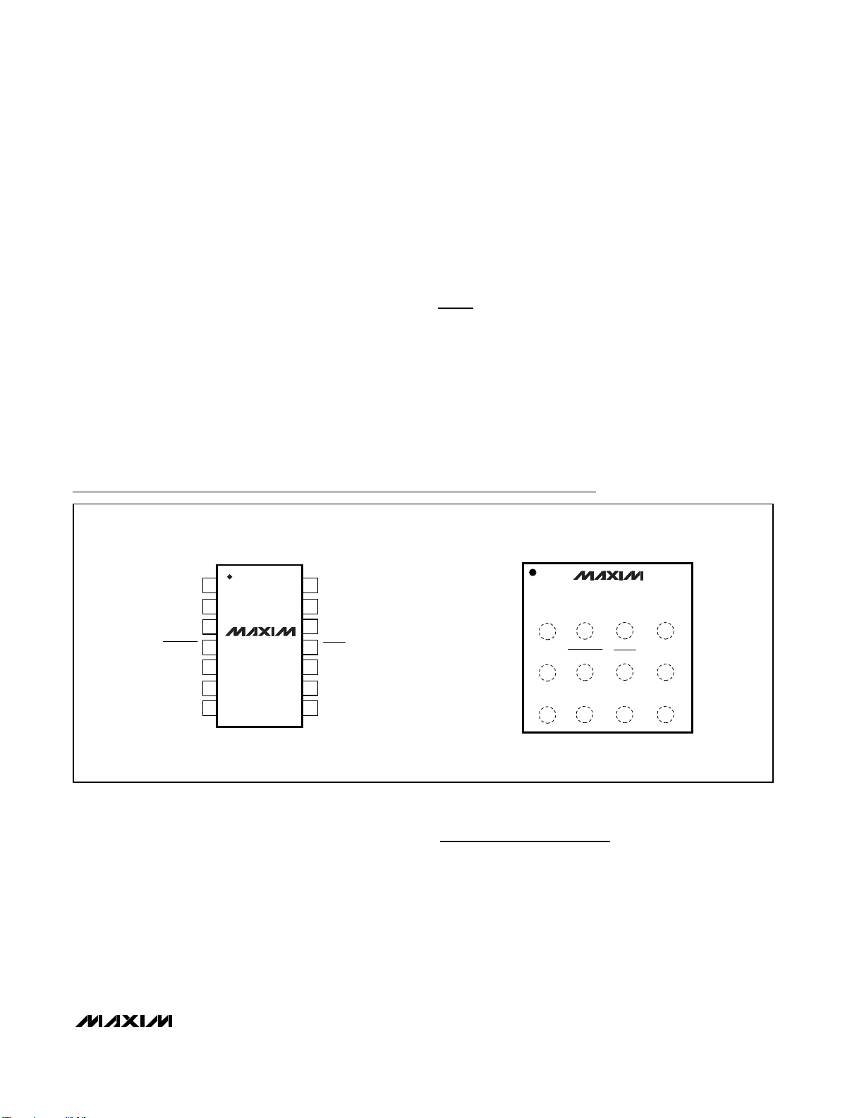
Pin Configurations
Chip Information
TRANSISTOR COUNT: 1601
PROCESS: BiCMOS
IEC 1000-4-2 is generally lower than that measured
using the Human Body Model. Figure 3 shows the IEC
1000-4-2 model. The Air-Gap Discharge test involves
approaching the device with a charged probe. The
contact-discharge method connects the probe to the
device before the probe is energized.
Machine Model
The Machine Model for ESD tests all pins using a
200pF storage capacitor and zero discharge resistance. Its objective is to emulate the stress caused by
contact that occurs with handling and assembly during
manufacturing. All pins require this protection during
manufacturing. After PC board assembly, the Machine
Model is less relevant to I/O ports.
Layout Considerations
The MAX3355E charge-pump switching frequency
makes proper layout important to ensure stability and
maintain the output voltage under all loads. For best
performance, minimize the distance between the
capacitors and the MAX3355E.
UCSP Applications Information
For the latest application details on UCSP construction, dimensions, tape-carrier information, printed circuit board techniques, bump-pad layout, and
recommended reflow temperature profile, as well as
the latest information on reliability testing results, refer
to Maxim Application Note: UCSP–A Wafer-Level
Chip-Scale Package available on Maxim’s web site at
www.maxim-ic.com/ucsp.
TOP VIEW
V
BUS
V
ID_OUT
STATUS1
STATUS2
1
2
CC
3
4
MAX3355E
5
6
7
14
C+
13
C-
12
GND
11
SHDNOFFVBUS
ID_IN
10
9
V
L
N.C.N.C.
8
TOP VIEW
A
B
C
1
ID_OUT STATUS1
V
CC
OFFVBUS SHDN
V
BUS
C+ C- GND ID_IN
MAX3355E
32
4
STATUS2
V
L
TSSOP
UCSP
Page 10

MAX3355E
±15kV ESD-Protected USB On-the-Go
Charge Pump and Comparators in UCSP
10 ______________________________________________________________________________________
Package Information
(The package drawing(s) in this data sheet may not reflect the most current specifications. For the latest package outline information
go to www.maxim-ic.com/packages
.)
MAX3355E Package Code: B12-1
12L, UCSP 4x3.EPS
PACKAGE OUTLINE, 4x3 UCSP
21-0104
1
F
1
Page 11
MAX3355E
±15kV ESD-Protected USB On-the-Go
Charge Pump and Comparators in UCSP
Maxim cannot assume responsibility for use of any circuitry other than circuitry entirely embodied in a Maxim product. No circuit patent licenses are
implied. Maxim reserves the right to change the circuitry and specifications without notice at any time.
Maxim Integrated Products, 120 San Gabriel Drive, Sunnyvale, CA 94086 408-737-7600 ____________________ 11
© 2003 Maxim Integrated Products Printed USA is a registered trademark of Maxim Integrated Products.
Package Information (continued)
(The package drawing(s) in this data sheet may not reflect the most current specifications. For the latest package outline information
go to www.maxim-ic.com/packages
.)
TSSOP4.40mm.EPS
 Loading...