

Page 1
General Description
The MAX3353E I2C-compatible USB On-the-Go (OTG)
regulated charge pump with switchable pullup/pulldown resistors allows peripherals and mobile devices
such as PDAs, cellular phones, and digital cameras to
be interconnected without a host PC.
The MAX3353E enables a system with an integrated
USB dual-role transceiver to function as a USB OTG
dual-role device. The charge pump in the MAX3353E
supplies V
BUS
power and signaling that is required by
the transceiver as defined in On-the-Go Supplement:
USB 2.0, Revision 1.0. The MAX3353E provides the
switchable pullup and pulldown resistors on D+ and Drequired for a dual-role device.
The MAX3353E integrates a regulated charge pump,
switchable pullup/pulldown resistors, and an I2C-compatible 2-wire serial interface. The device provides a
detector to monitor ID status and operates with logic
supply voltages (V
L
) between +1.65V and VCCand
charge-pump supply voltages (V
CC
) from +2.6V to
+5.5V. The charge pump supplies an OTG-compatible
output on V
BUS
while sourcing 8mA output current.
The MAX3353E enables USB OTG communication
between digital logic parts that cannot supply or tolerate
the +5V V
BUS
levels that USB OTG requires. By control-
ling and measuring V
BUS
using internal comparators,
this device supports USB OTG session request protocol
(SRP) and host negotiation protocol (HNP).
The MAX3353E has built-in ±15kV ESD protection circuitry
to guard V
BUS
, ID_IN, D+, and D-. The MAX3353E is
available in a 5 x 4 chip-scale package (UCSP™) and
16-pin TSSOP package.
Applications
Mobile Phones
PDAs
Digital Cameras
MP3 Players
Photo Printers
Features
♦ Ideal for Enabling USB Dual-Role Components for
USB OTG Protocol
♦ Charge Pump for V
BUS
Signaling and Operation
Down to +2.6V
♦ Level Translators Allow Low-Voltage System
Interface
♦ Internal V
BUS
Comparators and ID Detector
♦ Internal Switchable Pullup and Pulldown
Resistors for Host/Peripheral Functionality
♦ I
2
C-Compatible Bus Interface with Command and
Status Registers
♦ Interrupt Features
♦ ±15kV ESD Protection on ID_IN, V
BUS
, D+, and D-
♦ Supports SRP and HNP
♦ Available in 5 x 4 UCSP and 16-Pin TSSOP
MAX3353E
USB On-the-Go Charge Pump with Switchable
Pullup/Pulldown Resistors
________________________________________________________________ Maxim Integrated Products 1
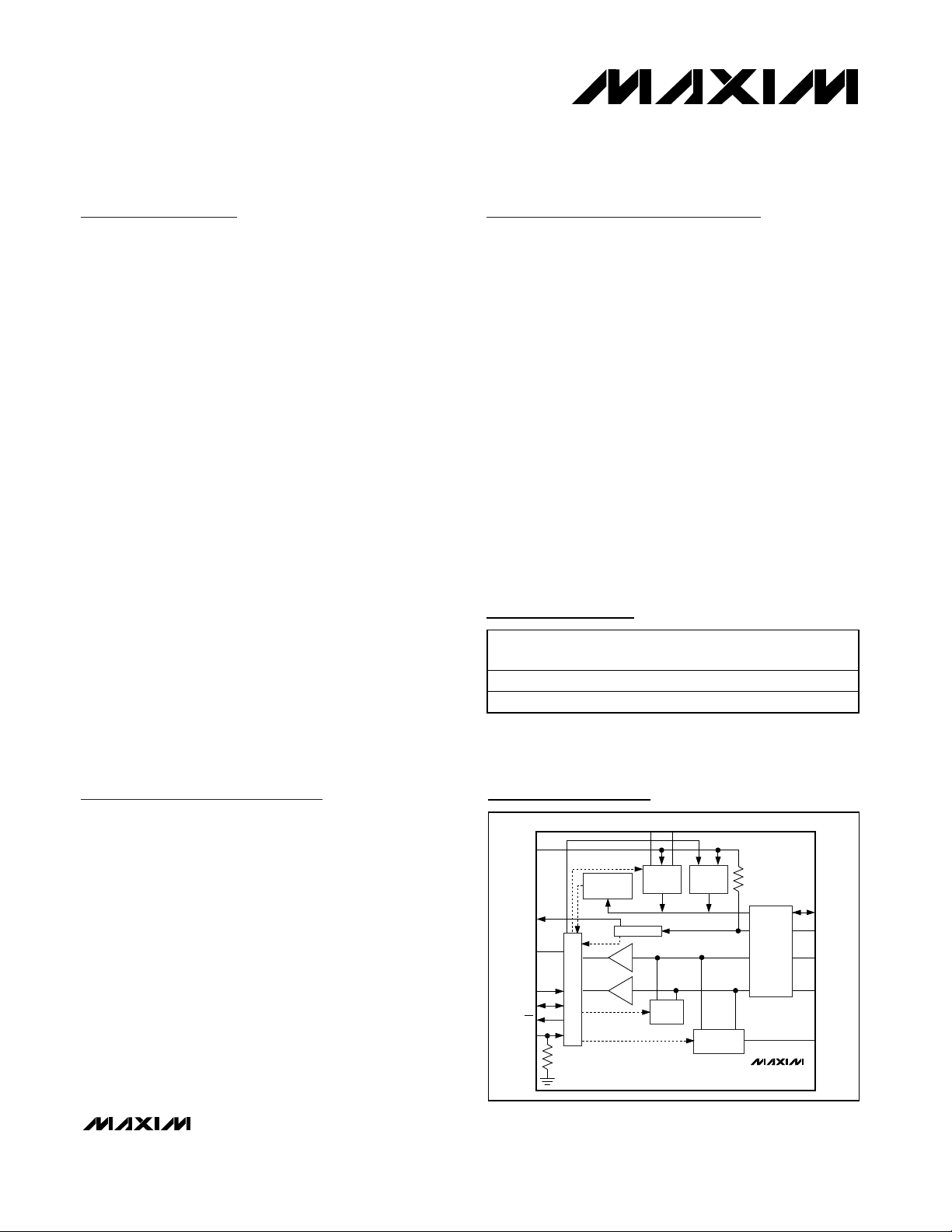
MAX3353E
PULLUP/DOWN
RESISTORS
CURRENT
GENERATOR
CHARGE
PUMP
C+ C-
V
BUS
COMPARATORS
I
2
C INTERFACE AND CONTROL LOGIC
ID DETECTOR
V
CC
V
L
ID_OUT
SCL
SDA
ADD
INT
V
BUS
ID_IN
D+
D-
V
TRM
SE0
DRIVER
200kΩ
±15kV
ESD
PROTECTION
110kΩ
Functional Diagram
Ordering Information
19-2845; Rev 1; 10/03
For pricing, delivery, and ordering information, please contact Maxim/Dallas Direct! at
1-888-629-4642, or visit Maxim’s website at www.maxim-ic.com.
UCSP is a trademark of Maxim Integrated Products, Inc.
PART
TEMP RANGE
PIN-
PKG
CODE
MAX3353EEUE
—
MAX3353EEBP-T
B20-4
Pin Configurations appear at end of data sheet.
Typical Applications Circuit appears at end of data sheet.
PACKAGE
-40°C to +85°C
-40°C to +85°C
16 TSSOP
5 x 4 UCSP
Page 2
MAX3353E
USB On-the-Go Charge Pump with Switchable
Pullup/Pulldown Resistors
2 _______________________________________________________________________________________
ABSOLUTE MAXIMUM RATINGS
ELECTRICAL CHARACTERISTICS
(VCC= +2.6V to +5.5V, VL= +1.65V to VCC, V
TRM
= +3V to +3.6V, C
FLYING
= 0.1µF, VCCdecoupled with 1µF capacitor to ground;
V
TRM
and VLdecoupled with 0.1µF capacitor to ground; C
VBUS
= 1µF (min), TA= T
MIN
to T
MAX
, unless otherwise noted. Typical
values are at V
CC
= +4V, VL= +1.8V, V
TRM
= +3.3V, and TA= +25°C.) (Notes 3, 4)
Stresses beyond those listed under “Absolute Maximum Ratings” may cause permanent damage to the device. These are stress ratings only, and functional
operation of the device at these or any other conditions beyond those indicated in the operational sections of the specifications is not implied. Exposure to
absolute maximum rating conditions for extended periods may affect device reliability.
(All voltages referenced to GND.)
V
CC,VL
, V
TRM
..........................................................-0.3V to +6V
D+, D-, ID_IN (Note 1)..............................................-0.3V to +6V
V
BUS
(Notes 1, 2) .....................................................-0.3V to +6V
C+..................................................................(V
CC
- 0.3V) to +6V
C-................................................................-0.3V to (V
CC
+ 0.3V)
INT, ID_OUT..................................................-0.3V to (V
L
+ 0.3V)
SDA, SCL, ADD .......................................................-0.3V to +6V
V
BUS
Output Short Circuit to Ground ....................... Continuous
Output Current (all other pins) .........................................±15mA
Continuous Power Dissipation (T
A
= +70°C)
16-Pin TSSOP (derate 9.4mW/°C above +70°C) .........755mW
5 x 4 UCSP (derate 7.8mW/°C above +70°C) .............625mW
Operating Temperature Range ...........................-40°C to +85°C
Storage Temperature Range .............................-65°C to +150°C
Junction Temperature......................................................+150°C
Lead Temperature (soldering 10s) .................................+300°C
Bump Temperature (soldering)
Infrared (15s) ...............................................................+200°C
Vapor Phase (20s) .......................................................+215°C
Note 1: 15kV ESD protected.
Note 2: V
BUS
can be backdriven to +6V.
)
Supply Voltage V
Logic Supply Voltage V
V
Supply Voltage V
TRM
VCC Operating Supply Current I
VCC Shutdown Supply Current I
V
Supply Current I
TRM
VL Input Current I
ID_OUT, INT Output Voltage High V
SDA, INT, ID_OUT Output
Voltage Low
SDA, SCL, ADD Input Voltage
High
SDA, SCL, ADD Input Voltage
Low
PARAMETER SYMBOL CONDITION MIN TYP MAX UNITS
CC
L
TRM
CC
CC(SHDN
VTRM
VL
OH
V
OL
V
IH
V
IL
Inp ut/Thr ee- S tate O utp ut Leakag e
C ur r ent ( S D A, S C L, INT)
ID_IN floating, V
V
BUS_CHG2
BUS_CHG1
= 0, V
BUS_DRV
= 0,
= 0,
BDISC_ACONN = 0
V
BUS_DRV
V
BUS_CHG2
= 1, V
= 0, I
BUS_CHG1
= 8mA
VBUS
= 0,
No activity on I2C serial bus 0.4 2 µA
DP_PULLDWN = 1, DP_PULLUP = 0,
DM_PULLDWN = 1, DM_PULLUP = 0
no activity on USB serial bus
No activity on I2C serial bus 1 µA
INT configured to push/pull; source current
= +1mA
I
LOAD
Sink current I
= -1mA 0.4 V
LOAD
INT configured to open drain ±1 µA
2.6 5.5 V
1.65 V
CC
3.0 3.6 V
73 100 µA
18 25 mA
1µA
V
- 0.4 V
L
0.67 x V
L
0.4 V
V
V
Page 3
MAX3353E
USB On-the-Go Charge Pump with Switchable
Pullup/Pulldown Resistors
_______________________________________________________________________________________ 3
ELECTRICAL CHARACTERISTICS (continued)
(VCC= +2.6V to +5.5V, VL= +1.65V to VCC, V
TRM
= +3V to +3.6V, C
FLYING
= 0.1µF, VCCdecoupled with 1µF capacitor to ground;
V
TRM
and VLdecoupled with 0.1µF capacitor to ground; C
VBUS
= 1µF (min), TA= T
MIN
to T
MAX
, unless otherwise noted. Typical
values are at V
CC
= +4V, VL= +1.8V, V
TRM
= +3.3V, and TA= +25°C.) (Notes 3, 4)
PARAMETER SYMBOL CONDITION MIN TYP MAX UNITS
ADD Pulldown Resistor 110 kΩ
ESD PROTECTION (V
, ID_IN, D+, D-)
BUS
ESD Protection
V
/ CHARGE-PUMP SPECIFICATIONS
B U S
(V
BUS_DRV
V
BUS
V
BUS
V
BUS
= 1, V
BUS_DISCHG
Output Voltage V
Output Current I
= 0, V
BUS_CHG1
BUSIVBUS
VBUS
Short-Circuit Current V
Output Ripple I
Efficiency VCC = 2.6V, I
Switching Frequency f 600 kHz
V
Voltage in Three-State
BUS
Mode
V
Pulldown Resistance V
BUS
V
Input Impedance V
BUS
V
AND CURRENT SOURCE SPECIFICATIONS (V
BUS
V
Output Voltage V
BUS
V
Current Source (Note 5) 450 600 850 µA
BUS
V
Current Gate Time V
BUS
BUS
COMPARATOR SPECIFICATIONS
V
BUS_VALID
Comparator
Threshold
V
BUS_VALID
Comparator
Hysteresis
SESSION_VALID Comparator
Threshold
SESSION_VALID Comparator
Hysteresis
B_SESSION_END Comparator
Threshold
B_SESSION_END Comparator
Hysteresis
SINGLE-ENDED RECEIVERS AND SE0 SPECIFICATIONS (D+, D-)
Low-Level Input Threshold 0.8 V
High-Level Input Threshold 2.0 V
Human Body Model ±15
IEC1000-4-2 Air-Gap Discharge ±11
IEC1000-4-2 Contact Discharge ±6
= 0, V
BUS_CHG2
= 0 to 8mA, C
= 0, unless otherwise noted.)
= 1µF 4.63 5.25 V
VBUS
8mA
shorted to GND 140 250 mA
BUS
= 8mA, C
VBUS
V
BUS_DRV
BUS_DRV
BUS_DRV
C
LOAD
C
LOAD
BUS_CHG1
= 0 0.2 V
= 0, V
= 0 40 100 kΩ
BUS_CHG1
= 15µF 2.1
= 95µF 1.9
= 1, V
= 1µF 100 mV
VBUS
= 8mA 80 %
VBUS
BUS_DISCHG
= 1, V
BUS_CHG2
= 1 3.2 5.1 6.5 kΩ
BUS_CHG2
= 0, V
BUS_DRV
= 0, V
BUS_DISCHG
= 0 (Note 5) 56 105 155 ms
4.40 4.55 4.63 V
20 mV
1.0 1.4 1.8 V
20 mV
0.4 0.5 0.6 V
35 mV
= 0)
kV
V
Page 4
MAX3353E
USB On-the-Go Charge Pump with Switchable
Pullup/Pulldown Resistors
4 _______________________________________________________________________________________
ELECTRICAL CHARACTERISTICS (continued)
(VCC= +2.6V to +5.5V, VL= +1.65V to VCC, V
TRM
= +3V to +3.6V, C
FLYING
= 0.1µF, VCCdecoupled with 1µF capacitor to ground;
V
TRM
and VLdecoupled with 0.1µF capacitor to ground; C
VBUS
= 1µF (min), TA= T
MIN
to T
MAX
, unless otherwise noted. Typical
values are at V
CC
= +4V, VL= +1.8V, V
TRM
= +3.3V, and TA= +25°C.) (Notes 3, 4)
TIMING CHARACTERISTICS
(VCC= +2.6V to +5.5V, VL = +1.65V to VCC, V
TRM
= +3V to +3.6V, C
FLYING
= 0.1µF, VCCdecoupled with 1µF capacitor to ground.
V
TRM
and VLdecoupled with 0.1µF capacitor to ground. C
VBUS
= 1µF (min), TA= T
MIN
to T
MAX
, unless otherwise noted. Typical val-
ues are at T
A
= +25°C, VCC= +4V, VL = +1.8V, V
TRM
= +3.3V.) (Notes 3, 4)
Hysteresis Voltage V
Output Voltage Low
(D+ and D- in SE0 state)
PULLUP/PULLDOWN RESISTOR SPECIFICATIONS (D+, D-, ID_IN)
Pulldown Resistor on D+
Pulldown Resistor on D-
Pullup Resistor on D+
Pullup Resistor on D-
D- Leakage Current
D+ Leakage Current
Input Impedance on D+/D-
ID_IN Pullup Resistor 140 200 270 kΩ
ID_IN Input Voltage Low 0.33 x V
ID_IN Input Voltage High 0.67 x V
PARAMETER SYMBOL CONDITION MIN TYP MAX UNITS
HYST
I
= -2.4mA 0.3 V
SINK
D P _P U LLD WN = 1, D P _P U LLU P = 0,
BD IS C _AC ON N = 0
D M _P U LLD WN = 1, D M _P U LLU P = 0,
BD IS C _AC ON N = 0
D P _P U LLD WN = 0, D P _P U LLU P = 1,
BD IS C _AC ON N = 0
D M _P U LLD WN = 0, D M _P U LLU P = 1,
D P _P U LLU P = 0, BDIS C _AC ONN = 0
D M _P U LLD WN = 0, D M _P U LLU P = 0,
BD IS C _AC ON N = 0
D P _P U LLD WN = 0, D P _P U LLU P = 0,
BD IS C _AC ON N = 0
D P _P U LLU P = 0, D P _PU LLDWN = 0,
D M _P U LLU P = 0, D M _PU LLDWN = 0,
BD IS C _AC ON N = 0
0.2 V
14.25 15.75 kΩ
14.25 15.75 kΩ
1.425 1.575 kΩ
1.425 1.575 kΩ
300 kΩ
CC
±1µA
±1µA
CC
V
V
Time to Assert D+ Pullup
Time to Assert SE0
Interrupt Propagation Delay (Note 6) 1 µs
V
BUS
INT Out Rise Time
PARAMETER SYMBOL CONDITION MIN TYP MAX UNITS
Rise Time
BDISC_ACONN = 1, ID_IN = GND
(A Device)
BDISC_ACONN = 1,
ID_IN = floating (B Device)
From 0 to 4.4V; C
V
INT out push/pull configured,
C
BUS_DRV
LOAD
= 1
= 50pF
= 1µF; I
LOAD
VBUS
= 8mA;
1ms
0.025 0.061 1 ms
100 ms
20 ns
Page 5
MAX3353E
USB On-the-Go Charge Pump with Switchable
Pullup/Pulldown Resistors
_______________________________________________________________________________________ 5
TIMING CHARACTERISTICS (continued)
(VCC= +2.6V to +5.5V, VL = +1.65V to VCC, V
TRM
= +3V to +3.6V, C
FLYING
= 0.1µF, VCCdecoupled with 1µF capacitor to ground.
V
TRM
and VLdecoupled with 0.1µF capacitor to ground. C
VBUS
= 1µF (min), TA= T
MIN
to T
MAX
, unless otherwise noted. Typical val-
ues are at T
A
= +25°C, VCC= +4V, VL = +1.8V, V
TRM
= +3.3V.) (Notes 3, 4)
I2C/SMBUS-COMPATIBLE TIMING SPECIFICATIONS
(VCC= +2.6V to +5.5V, VL = +1.65V to VCC, V
TRM
= +3V to +3.6V, C
FLYING
= 0.1µF, VCCdecoupled with 1µF capacitor to ground.
V
TRM
and VLdecoupled with 0.1µF capacitor to ground. C
VBUS
= 1µF (min). TA= T
MIN
to T
MAX
, unless otherwise noted. Typical val-
ues are at V
CC
= +4V, VL = +1.8V, V
TRM
= +3.3V, and TA= +25°C.) (Notes 3, 4)
Note 3: All currents into the device are negative; currents out of the device are positive. All voltages are referenced to device
ground unless otherwise specified.
Note 4: Parameters are 100% production tested at +25°C, limits over temperature are guaranteed by design.
Note 5: The V
BUS
current source and current gate time vary together with process and temperature such that the resulting V
BUS
pulse is guaranteed to drive a <13µF load to a voltage >2.0V, and to drive a >96µF load to a volatge <2.2V. See the SRP
V
BUS
Pulsing section for an explanation of this self-timed pulse.
Note 6: Guaranteed by design, not production tested.
Note 7: A master device must provide a hold time of at least 300ns for the SDA signal to bridge the undefined region of SCL’s falling
edge.
Note 8: C
B
is total capacitance of one bus line in pF. Tested with CB= 400pF.
Note 9: Input filters on SDA, SCL, and ADD suppress noise spikes less than 50ns.
PARAMETER SYMBOL CONDITION MIN TYP MAX UNITS
INT Out Fall Time C
ID_OUT Rise Time C
ID_OUT Fall Time C
Time to Exit Shutdown 500 µs
Time to Enter Shutdown 1000 µs
= 50pF 20 ns
LOAD
= 50pF 30 ns
LOAD
= 50pF 10 ns
LOAD
PARAMETER SYMBOL CONDITION MIN TYP MAX UNITS
Serial Clock Frequency f
Bus Free Time Between Stop and
Start Conditions
Start Condition Hold Time t
Stop Condition Setup Time t
Clock Low Period t
Clock High Period t
Data Setup Time t
Data Hold Time t
Maximum Receive SCL/SDA Rise
Time
Minimum Receive SCL/SDA Rise
Time
Maximum Receive SCL/SDA Fall
Time
Minimum Receive SCL/SDA Fall
Time
Transmit SDA Fall Time (Note 4)
Pulse Width of Suppressed Spike t
SCL
t
BUF
HD:STA
SU:STO
LOW
HIGH
SU:DAT
HD:DAT
t
R
t
R
t
F
t
F
t
F
t
F
SP
DC 400 kHz
1.3 µs
0.6 µs
0.6 µs
1.3 µs
0.6 µs
100 ns
(Note 7) 0 0.9 µs
(Note 8) 300 ns
(Note 8) 20 + 0.1C
B
(Note 8) 300 ns
(Note 8) 20 + 0.1C
CB = 400pF, I
CB = 50pF, I
= 3mA, VL ≥ 2.5V 20 + 0.1C
SDA
= 3mA, VL < 2.5 20 + 0.1C
SDA
B
B
B
250
250
(Note 9) 50 ns
ns
ns
ns
Page 6
MAX3353E
USB On-the-Go Charge Pump with Switchable
Pullup/Pulldown Resistors
6 _______________________________________________________________________________________
Typical Operating Characteristics
(VCC= +3V, VL= +2.5V, C
FLYING
= 0.1µF, C
VBUS
= 1µF (ESR
CVBUS
= 0.1Ω), TA= +25°C.)
0
40
20
80
60
100
120
050
INPUT CURRENT
vs. OUTPUT CURRENT
MAX3353 toc01
OUTPUT CURRENT (mA)
INPUT CURRENT (mA)
2010 30 40
VCC = 2.6V
V
CC
= 3.3V
V
CC
= 4.2V
4.00
4.50
4.25
4.75
5.00
5.25
050
V
BUS
OUTPUT VOLTAGE
vs. V
BUS
OUTPUT CURRENT
MAX3353 toc02
OUTPUT CURRENT (mA)
V
BUS
OUTPUT VOLTAGE (V)
2010 30 40
VCC = 2.6V
VCC = 4.2V
V
CC
= 3.3V
4.70
4.80
4.75
4.85
4.90
2.5
V
BUS
OUTPUT VOLTAGE
vs. INPUT VOLTAGE
MAX3353 toc03
INPUT VOLTAGE (V)
V
BUS
OUTPUT VOLTAGE (V)
4.0
3.5
3.0
5.0
4.5
5.5
I
VBUS
= 8mA
I
VBUS
= 0
MAX3353 toc04
200μs/div
I
CC
5mA/div
SCL
5V/div
TIME TO ENTER SHUTDOWN
MAX3353 toc05
100μs/div
I
CC
10mA/div
SCL
5V/div
TIME TO EXIT SHUTDOWN
MAX3353 toc06
40ms/div
V
BUS
1V/div
V
BUS
1V/div
CL = 10μF
CL = 96μF
V
BUS
WITH CAPACITIVE LOAD
65.0
67.0
66.5
66.0
65.5
67.5
68.0
-40 85
V
BUS
INPUT IMPEDANCE
vs. TEMPERATURE
MAX3353 toc07
TEMPERATURE (°C)
V
BUS
INPUT IMPEDANCE (kΩ)
10-15
35
60
16
18
17
19
20
-40 85
SUPPLY CURRENT
vs. TEMPERATURE
MAX3353 toc08
TEMPERATURE (°C)
SUPPLY CURRENT (mA)
10-15
35
60
I
VBUS
= 8mA
VCC = 2.6V
VCC = 3.3V
VCC = 4.2V
Page 7
Detailed Description
The MAX3353E integrates a regulated charge pump,
switchable pullup/pulldown resistors, and an I2Ccompatible 2-wire serial interface. The internal level
shifter allows the device to operate with logic supply voltages (VL) between +1.65V and VCC. The MAX3353E’s
OTG-compliant charge pump operates with input supply
voltages (VCC) from +2.6V to +5.5V and supplies an
OTG-compatible output on V
BUS
while sourcing 8mA
output current.
The MAX3353E level-detector comparators monitor important V
BUS
voltages needed to support SRP and HNP and
provides an interrupt output signal for OTG events that
require action. The V
BUS
power-control block performs the
various switching functions required by an OTG dual-role
device and is programmable by system logic.
For OTG operation, D+ and D- are connected to switchable pulldown resistors (host) and switchable pullup
resistors (peripheral) controlled by internal registers.
Charge Pump
The MAX3353E’s OTG-compliant charge-pump operates
with input supply voltages (VCC) from +2.6V to +5.5V
and supplies an OTG-compatible output on V
BUS
with
the capability of sourcing 8mA (min) output current.
When V
BUS
is not providing power, an input impedance
of no more than 100kΩ and no less than 40kΩ to GND is
present on V
BUS
. When V
BUS
provides power, the rise
time on V
BUS
from 0 to 4.4V is no longer than 100ms
when driving a constant current load of 8mA and an
external load capacitance of 13µF.
During a continuous short circuit on V
BUS
, the chargepump output is current limited to 140mA (typ). Thermalshutdown circuitry turns off the charge pump if the die
temperature exceeds +150°C and restarts when the die
cools to 140°C.
Level Shifters
Internal level shifters allow the system-side interface to
run at logic supply voltages as low as 1.65V. Interface
logic signals are referenced to the voltage applied to VL.
MAX3353E
USB On-the-Go Charge Pump with Switchable
Pullup/Pulldown Resistors
_______________________________________________________________________________________ 7
Pin Description
PIN
TSSOP UCSP
1C5VCCPower-Supply Input. VCC input range is +2.6V to +5.5V. Bypass VCC to GND with a 1µF capacitor.
2D5V
3 D4 SDA Serial Data Input/Output. I2C bus serial data input/open-drain output can be driven above VL.
4 C3 ADD
5 D3 SCL Serial Clock Input. I2C bus serial clock input. Can be driven above VL.
6D2INT
7 D1 ID_OUT Device ID Output. Output of ID_IN level translated to VL.
8C1V
9 B1 D- USB D- (±15kV ESD Protected)
10 A1 D+ USB D+ (±15kV ESD Protected)
11 A2 ID_IN
12 — N.C. No Connection. Not internally connected.
13 A3 GND Ground
14 A4 C- Charge-Pump Capacitor Negative Connection
15 A5 C+ Charge-Pump Capacitor Positive Connection
16 B5 V
NAME FUNCTION
Logic Supply. VL sets the logic output high voltage and logic input high threshold for SDA, SCL,
L
INT, and ID_OUT. V
Address Select Input. Address selection for the I
110kΩ pulldown resistor (see the 2-Wire I
Interrupt Output. INT is an active-low output and can be set either open-drain or push/pull output
through control register 1 (default = open drain).
Termination Supply Input. Connect +3V to +3.6V supply voltage for internal USB pullup resistors.
TRM
Bypass V
Device ID Input. Internally pulled up to V
can be read through the I
OTG Bus Supply. Provides power to the bus. V
BUS
GND with a 1µF capacitor.
TRM
can range from +1.65V to VCC. Bypass VL to GND with a 0.1µF capacitor.
L
2
C-compatible interface. ADD has an internal
2
C Compatible Serial Interface section for details).
to GND with a 0.1µF capacitor.
. ID_IN logic state is VL level translated to ID_OUT and
2
C interface (±15kV ESD protected).
CC
can be back-driven to +6V. Bypass V
BUS
BUS
to
Page 8
MAX3353E
V
BUS
Level-Detection Comparators
Comparators drive status register bits 0, 1, and 2 to
indicate these important USB OTG V
BUS
voltage levels:
•V
BUS
is valid (V
BUS
> 4.6V)
• A USB session is valid (V
BUS
> 1.4V)
• A USB session is ended (V
BUS
< 0.5V)
The 4.6V comparator sets bit 0 in status register
V
BUS_VALID
to 1 if V
BUS
> 4.6V. The A Device uses the
V
BUS
valid status bit (V
BUS_VALID
) to determine if the B
Device is sinking too much current (i.e., is not supported).
The interrupt can be associated to either a positive or a
negative transition. The 1.4V comparator sets bit 1 of status register SESSION_VALID to 1 if V
BUS
> 1.4V. This status bit indicates that a data transfer session is valid and
the interrupt can be associated to either a positive or a
negative transition. The session-end comparator sets bit
2 in the status register SESSION_END to a 1 when V
BUS
< 0.5V, and generates an interrupt when V
BUS
falls below
0.5V. Figure 1 shows the level-detector comparators.
Interrupt Logic
When OTG events require action, the MAX3353E provides an interrupt output signal on INT. An interrupt is
triggered (INT goes low) when one of the conditions
specified by the interrupt-mask register and interruptedge register is verified. INT stays active until the interrupt is cleared by reading the interrupt latch register.
Shutdown
In shutdown mode, the MAX3353E’s quiescent current
is reduced to less than 2µA. Bit 0 in control register 2
controls the shutdown feature. Setting bit 0 = 1 places
the device in shutdown mode (Figure 2, Table 5). When
in shutdown, the MAX3353E’s charge-pump current
generator and V
BUS
detection comparators are turned
off. During shutdown, the I2C serial interface is fully
functional and registers can be read from or written to.
ID_IN and ID_OUT are both functional in shutdown.
V
BUS
Power Control
V
BUS
is a dual-function I/O that can supply USB OTG-
compliant voltage to the USB. The V
BUS
power-control
block performs the various switching functions required
by an OTG dual-role device. This action is programmed
by the system logic using internal register control bits in
control register 2.
• Discharge V
BUS
through a resistor to ensure a ses-
sion is not in progress.
• Charge V
BUS
through an internal current generator
to initiate SRP (session request protocol).
• Connect the charge pump to V
BUS
to provide power
on V
BUS
.
Bit 0 (SDWN) in control register 2 is used to place the
MAX3353E in normal operation or shutdown mode.
Setting bit 1 (V
BUS_CHG1
) issues a timed pulse on V
BUS
suitable for implementing the session request protocol
(see the SRP V
BUS
Pulsing section). The pulse is created
by turning a current source – supplied by VCCand connected to V
BUS
– on and off. Setting control register bit
2 (V
BUS_CHG2
) to 1 charges VBUS through the current
source continuously. Setting V
BUS_CHG2
to zero discon-
nects the current source. Bit 3 (V
BUS_DRV
) turns the
USB On-the-Go Charge Pump with Switchable
Pullup/Pulldown Resistors
8 _______________________________________________________________________________________
Figure 1. Comparator Network Diagram
Figure 2. Power-Control Block Diagram
V
BUS
V
4.6V
1.4V
0.5V
V
CC
CURRENT SOURCE
CHARGE
PUMP
ON/OFF
CURRENT
76543210
00000001
DEFAULT
(POWER-ON)
VALUES
NOTE: SWITCHES ARE SHOWN IN THEIR DEFAULT
(POWER-ON) POSITIONS. A "1" CLOSES A SWITCH.
GATE
TIMER
0 = OPERATING MODE
1 = SHUTDOWN MODE
BUS_VALID
SESSION_VALID
SESSION_END
67kΩ
5kΩ
CONTROL REGISTER 2
V
BUS
Page 9

charge pump on and off to power V
BUS
. Bit 4 in control
register 2 (V
BUS_DISCHG
) is used to discharge V
BUS
through a 5kΩ resistor. Figure 2 and Table 2 show
power control.
Autoconnect and Autoresponse
USB OTG defines the HNP, where the default host (A
Device) can pass the host responsibilities off to the
default peripheral (B Device). This protocol can be handled entirely by the firmware and controlling logic that drives the OTG transceiver. The MAX3353E has the option
to automatically perform some of the required signaling
for some of the timing-critical events in the HNP process.
The automatic signaling used by the A Device, when it
transfers host control to the B Device, is defined by the
OTG transceiver supplement and is known as autoconnect. Autoconnect allows the transceiver to automatically
connect the A Device’s D+ pullup resistor during HNP.
Autoconnect is enabled when the MAX3353E is configured as an A Device (ID_IN = 0) and the BDISC_ACONN
control bit is set.
The MAX3353E also has the capability to automate the
signaling used by the B Device when it assumes host
control from the A Device. This autoresponse is not specified by the OTG-transceiver supplement. Autoresponse
causes the B Device to automatically assert a bus reset
by driving a single-ended zero (SE0: both D+ and D- driven low) onto USB in response to the A Device connecting its D+ pullup resistor. Autoresponse is enabled when
the MAX3353E is configured as a B Device and the
BDISC_ACONN control bit is set.
Note: In a system, D+ and D- are also driven by a transceiver in an ASIC or other device. The autoresponse
mode should not be used unless the system designer
can ensure that there is no bus conflict between the
transceiver and the MAX3353E driving USB to SE0.
Autoconnect Details
When the MAX3353E is configured as an A Device
(ID_IN = GND), it can enable autodetect by setting
BDISC_ACONN to one. This should be done after the
USB is in the suspend state (>3ms with no traffic). The
MAX3353E monitors D+/D- for an SE0. The presence of
the SE0 indicates that the B Device has disconnected
its pullup resistor, the first step in HNP. When SE0 is
detected, the MAX3353E automatically turns on its
internal pullup resistor to the D+ line within 3ms. There
are two ways for firmware to ascertain that the
MAX3353E has automatically turned on its D+ pullup
during HNP:
1) The A_HNP status bit goes high when the D+ pullup
is automatically connected during HNP
2) The A_HNP_EN control bit is set, and an interrupt is
issued as the D+ pullup is connected (see also the
Interrupt Logic section).
By clearing BDISC_ACONN bit, the D+ pullup is disconnected. After a successful autoconnect operation, the
firmware should set the DP_PULLUP control bit before
clearing the BDISC_ACONN bit; this ensures that the
D+ pullup remains connected.
Note: The autoconnect works only if MAX3353E is not
in shutdown.
Autoresponse Details
When the MAX3353E is configured as a B Device
(ID_IN = open), setting the BDISC_ACONN control bit
enables the autoresponse feature. Using this feature,
the MAX3353E automatically issues a USB bus reset
when the A Device becomes a peripheral. Firmware
can take advantage of the autoresponse feature of the
MAX3353E by doing the following:
• Ensure that the system transceiver is in USB-sus-
pend mode. Wait until the USB-suspend conditions
are met (no USB activity for >3ms). Enable autoresponse. Set the BDISC_ACONN control bit. Signal
a USB disconnect. Firmware clears the DP_PULLUP
control bit, which disconnects the D+ pullup resistor. At this point, the MAX3353E waits at least 25µs
before enabling its internal USB line monitor to
detect if the A Device has attached its D+ pullup;
this ensures that the D+ line is not high due to the
residual effect of the B Device pullup. When the A
Device has connected its D+ pullup, the MAX3353E
issues a bus reset (SE0) and the B_HNP status bit
goes high.
• Wait for B_HNP to go high; output SE0 from the
ASIC or other device on D+/D-. Disable autoresponse. By clearing BDISC_ACONN bit, the SE0
generator is turned off. The SE0 is maintained by the
system USB transceiver.
Note: The autoresponse works only if the MAX3353E is
not in shutdown.
SRP V
BUS
Pulsing
Session request protocol (SRP) is designed to allow
the A Device (default host) to conserve power by turning off V
BUS
when there is no USB traffic. The B Device
(default peripheral) can request the A Device to turn
V
BUS
on and initiate a new session through SRP.
The B Device must initiate SRP in two ways: data-line
and V
BUS
pulsing. Firmware is responsible for turning
on and off the pullup resistor on D+ to implement
data-line pulsing. Firmware can also be used to turn on
and off a current source to implement V
BUS
pulsing.
MAX3353E
USB On-the-Go Charge Pump with Switchable
Pullup/Pulldown Resistors
_______________________________________________________________________________________ 9
Page 10
MAX3353E
The MAX3353E also has a special feature that allows it
to control the timing of the V
BUS
pulse.
Since an OTG device could be plugged into a PC, the
V
BUS
pulse must be particularly well controlled to prevent
damage to a PC host. For this reason, V
BUS
pulsing is
done by turning on and off a current source. The V
BUS
pulse must be timed so it drives a 13µF load (when it is
connected to the A Device) to a voltage greater than
2.1V, and it drives a >96µF load (when it is connected to
a standard PC) to a voltage less than 2.0V.
Firmware can control the current source and the timing
of the V
BUS
pulse through the V
BUS_CHG2
control bit.
The MAX3353E also has the capability to time the pulse
itself. Firmware initiates the self-timed V
BUS
pulse by
setting the V
BUS_CHG1
control bit to 1.
The internal timer and current generator guarantee that
the V
BUS
voltage goes above 2.1V if C
VBUS
< 13µF
within 90ms and stands below 2.0V if C
VBUS
>
96µF.
Once the time has elapsed, if another V
BUS
pulse is
required, it is necessary to clear the V
BUS_CHG1
bit and
then set it again.
Note: SRP V
BUS
pulsing and its associated current gen-
erator work only if the MAX3353E is not in shutdown.
Data-Line Pullup and Pulldown Resistance
For OTG operation, D+ and D- are connected to switchable pulldown resistors (host) and switchable pullup
resistors (peripheral). Data-line pullup/pulldown resistors
are individually controlled through data bits 4 through 7 in
control register 1. Two 15kΩ pulldown resistors allow the
device to be set as a host and are asserted by bits 6 and
7. The 1.5kΩ pullup resistor is applied to the data lines
through SW1 and SW2, which are controlled by bits 4 and
5. D+ pullup has higher priority to avoid direct connection
of D+ and D-. Each of the control bits controls a designated switch; therefore, pullup and pulldown switches can
be asserted at the same time. A simplified schematic of
the switching network is shown in Figure 3.
The bidirectional D+ and D- lines are ESD protected to
±15kV, reducing external components in many applications.
Applications Information
2-Wire I2C-Compatible Serial Interface
A register file that interfaces to the control logic uses a
simple 2-wire interface operating up to 400kHz to control the various switches and modes.
Serial Addressing
The MAX3353E operates as a slave that sends and
receives control and status signals through an I2Ccompatible 2-wire interface. The interface uses a serial
data line (SDA) and a serial clock line (SCL) to achieve
USB On-the-Go Charge Pump with Switchable
Pullup/Pulldown Resistors
10 ______________________________________________________________________________________
Figure 3. Pullup and Pulldown Resistors Network
Figure 4. 2-Wire Serial Interface Timing Details
V
TRM
1.5kΩ
SW2 SW1
15kΩ
SW4
76543210
0000
DEFAULT
(POWER ON)
VALUES
15kΩ
SW3
CONTROL REGISTER 1
NOTE: SWITCHES ARE SHOWN IN THEIR DEFAULT
(POWER-ON) POSITIONS. A "1" CLOSES A SWITCH.
BIT 4
BIT 5
0
0
1
1 1 CLOSED OPEN
0000
SW1
0
OPEN
1
OPEN
0
CLOSED
D+
D-
GND
SW2
OPEN
CLOSED
OPEN
SCL
t
SDA
HD:STA
t
F
t
LOW
t
SU:DAT
t
R
t
HIGH
t
HD:DAT
t
SU:STO
t
BUF
Page 11
bidirectional communication between master(s) and
slave(s). A master (typically a microcontroller) initiates
all data transfers to and from the MAX3353E and generates the SCL clock that synchronizes the data transfer (Figure 4).
The MAX3353E SDA line operates as both an input and
an open-drain output. A pullup resistor (4.7kΩ typ) is
required on SDA. The MAX3353E SCL line operates
only as an input. A pullup resistor (4.7kΩ typ) is
required on SCL if there are multiple masters on the 2wire interface, or if the master in a single-master system
has an open-drain SCL output.
Each transmission consists of a START condition
(Figure 5) sent by a master, followed by the MAX3353E
7-bit slave address plus R/W bit (Figure 6), a register
address byte, one or more data bytes, and finally a
STOP condition (Figure 5).
Start and Stop Conditions
Both SCL and SDA remain high when the interface is
not busy. A master signals the beginning of a transmission with a START (S) condition by transitioning SDA
from high to low while SCL is high. When the master
has finished communicating with the slave, it issues a
STOP (P) condition by transitioning the SDA from low to
high while SCL is high. The bus is then free for another
transmission (Figure 5).
Bit Transfer
One data bit is transferred during each clock pulse.
The data on the SDA line must remain stable while SCL
is high (Figure 7).
Acknowledge
The acknowledge bit is the clocked ninth bit that the
recipient uses to handshake receipt of each byte of
data (Figure 8). Thus, each byte transferred effectively
requires 9 bits. The master generates the 9th clock
pulse, and the recipient pulls down SDA during the
acknowledge clock pulse, such that the SDA line is stable low during the high period of the clock pulse. When
the master is transmitting to the MAX3353E, the
MAX3353E generates the acknowledge bit because it
is the recipient. When the MAX3353E is transmitting to
the master, the master generates the acknowledge bit
because the master is the recipient.
Slave Address
The MAX3353E has a 7-bit-long slave address. The
eighth bit following the 7-bit slave address is the R/W
bit. It is low for a write command, high for a read command. The first 6 bits (MSBs) of the MAX3353E slave
address are always 010110. Select slave address bit
A0 by connecting the address input ADD to VL, GND,
or leave floating (ADD is internally pulled to GND
through a 110kΩ resistor). The MAX3353E has two possible slave addresses (Table 1). As a result, only two
MAX3353E devices can share the same interface.
Write Byte Format
A write to the MAX3353E comprises the transmission of
the MAX3353E’s slave address with the R/W bit set to
zero, followed by 2 bytes of information. The first byte
of information is the command byte that determines
which register of the MAX3353E is to be written by the
second byte. The second byte is the data that goes into
the register that is set by the first byte. Figure 9 shows
the typical write byte format.
Read Byte Format
A read from the MAX3353E comprises the transmission
of the MAX3353E’s slave address (from the master)
with the R/W bit set to zero, followed by one byte containing the address of the register, from which the master is going to read data, and then followed by
MAX3353E’s slave address again with the R/W bit set
to one. After that one byte of data is being read by the
master. Figure 10 shows the read byte format that must
be used. To read many contiguous registers, multiple
accesses are required.
Registers
Control Registers (10h, 11h)
There are two read/write control registers. Control register 1 is used to set D+, D- pullup or pulldown, and to
set interrupt output to open-drain or push-pull. Control
register 2 is the bus control register used to control the
bus operation and put the device into shutdown mode.
(Tables 3, 4, and 5.)
Status Register (13h)
The status register is a read-only register for determining
valid bus and session comparator thresholds, ID_IN status, and HNP success. Tables 6 and 7 show status register address map, bit configuration, and description.
MAX3353E
USB On-the-Go Charge Pump with Switchable
Pullup/Pulldown Resistors
______________________________________________________________________________________ 11
Figure 5. Start and Stop Conditions
SDA
SCL
S
START
CONDITION
P
STOP
CONDITION
Page 12
MAX3353E
USB On-the-Go Charge Pump with Switchable
Pullup/Pulldown Resistors
12 ______________________________________________________________________________________
Figure 6. Slave Address
Figure 7. Bit Transfer
Figure 8. Acknowledge
Figure 10. Read Byte Format
Figure 9. Write Byte Format
SDA
START
SCL
SDA
SCL
DATA LINES STABLE,
DATA VALID
S PART ADDRESS R/W ACK REGISTER ADDRESS ACK
A
6A5A4A3A2A1A0
A
7A6A5A4A3A2A1A0
Where:
Slave address: Part address P: Stop condition
Register address: Selecting which register to write to ACK: Acknowledge bit from the slave
Data: Data byte being read by the master NACK: Not acknowledged bit from the master
R/W: Read/Write (R/W = 1: Read; R/W = 0: Write) Blank: Master transmission
S: Start condition Shaded: Slave transmisstion
0
MSB
CHANGE OF
DATA ALLOWED
1
7 bits W 8 bits
DATA ACK P
8 bits
0
1
1
SDA BY
TRANSMITTER
SDA BY
RECEIVER
0A0
LSB
START
CONDITION
SCL
S
CLOCK PULSE FOR ACKNOWLEDGMENT
12 8 9
R/W
ACK
0
S PART ADDRESS R/W ACK REGISTER ADDRESS ACK
A
6A5A4A3A2A1A0
RS PART ADDRESS R/W ACK DATA NACK
A
6A5A4A3A2A1A0
Where:
Slave address: Part address P: Stop condition
Register address: Selecting which register to write to ACK: Acknowledge bit from the slave
Data: Data byte being read by the master NACK: Not acknowledged bit from the master
R/W: Read/Write (R/W = 1: Read; R/W = 0: Write) Blank: Master transmission
S: Start condition Shaded: Slave transmisstion
7 bits 8 bits
7 bits 8 bits
0
00
01
1
P
Page 13
Interrupt Registers (14h, 15h, 16h)
There are three interrupt registers. Interrupt mask register is a read/write register used to enable interrupts and
read status of interrupts. Interrupt edge register is a
read/write register for setting and determining interrupts for positive and negative edges. Interrupt latch
register is a read only register to check and validate
interrupt requests. Table 8 shows the interrupt mask,
MAX3353E
USB On-the-Go Charge Pump with Switchable
Pullup/Pulldown Resistors
______________________________________________________________________________________ 13
Table 1. MAX3353E Address Map
Table 2. Register Address Map
ADD PIN
Float or
GND
V
L
A
A
6
0101100
0101101
ADDRESS BITS
A
5
4
A
A
3
2
A
A
1
0
NAME ADD BIT 7 BIT 6 BIT 5 BIT 4 BIT 3 BIT 2 BIT 1 BIT 0
Manufacturer
Register 0
Manufacturer
Register 1
Manufacturer
Register 2
Manufacturer
Register 3
Product ID
Register 0
Product ID
Register 1
Product ID
Register 2
Product ID
Register 3
Reserved 08h-0Fh — — ——————
Control
Register 1
Control
Register 2
Reserved 12h — — ——————
Status
Register
Inter r up t M ask 14h — — A_HNP_EN
Inter r up t E d g e15h——————
Interrupt
Latch
Reserved 17h -Ffh — — ——————
00h01101010
01h00001011
02h01010011
03h00110011
04h01001000
05h01011010
06h01000010
07h00000001
10h
11h — — —
13h — B_HNP A_HNP ID_FLOAT ID_GND
16h A_HNP_RQ
DM_
PULLDWN
DP_
PULLDWN
ID_
FLOAT_RQ
DM_
PULLUP
ID_
GND_RQ
DP_
PULLUP
V
BUS_
DISCHG
ID_
FLOAT_EN
SESSION_
END_RQ
—
V
BUS_DRVVBUS_CHG2VBUS_CHG1
ID_
GND_EN
SESSION_
VALID_RN
BDISC_
ACONN
SESSION_
END
SESSION_
END_EN
V
BUS_
VALID_RN
IRQ_MODE —
SDWN
SESSION_
VALID
SESSION_
VALID_EN
SESSION_
VALID_ED
SESSION_
VALID_RP
V
BUS_VALID
V
BUS_
VALID_EN
V
BUS_
VALID_ED
V
BUS_
VALID_RP
Page 14
MAX3353E
interrupt edge, and interrupt latch address maps. Bit
configuration is shown in Tables 9, 10, and 11.
Manufacturer and ID Register Address Map
The manufacturer and ID registers are read-only registers (Table 12).
External Capacitors
Five external capacitors are recommended for proper
operation. Bypass VL and V
TRM
to GND with a 0.1µF
ceramic capacitor. Bypass V
BUS
and VCCto GND with a
1µF low-ESR ceramic capacitor. For the internal charge
pump, use a 0.1µF ceramic capacitor between C+ and C-.
USB On-the-Go Charge Pump with Switchable
Pullup/Pulldown Resistors
14 ______________________________________________________________________________________
Table 3. Control Register Address Map
Table 4. Control Register 1 (10h)
Table 5. Control Register 2 (11h)
Table 6. Status Register Address Map
(—) = don’t know
REGISTER ADDRESS
Control 1 10h 00000000
Control 2 11h 00000001
BIT 7 BIT 6 BIT 5 BIT 4 BIT 3 BIT 2 BIT 1 BIT 0
BIT
NUMBER
0 — Not used
1 IRQ_MODE
2
3 — Not used
4 DP_PULLUP
5 DM_PULLUP
6
SYMBOL OPERATION
Interrupt pin open-drain/push-pull:
0 = open drain
1 = push/pull
BDISC_
ACONN
DP_
PULLDWN
0 = disable
1 = enable
D+ pullup (high priority)
0 = D+ pullup unconnected
1 = D+ pullup connected
D- pullup:
0 = D- pullup unconnected
1 = D- pullup connected
D+ pulldown:
0 = D+ pulldown unconnected
1 = D+ pulldown connected
POWER-UP REGISTER STATUS
BIT
NUMBER
0 SDWN
1V
2V
3V
SYMBOL OPERATION
Puts part in shutdown mode:
0 = operating
1 = shutdown mode
Charge V
generator for 105ms:
BUS_CHG1
BUS_CHG2
BUS_DRV
0 = current generator OFF
1 = current generator ON
(automatically turned off after
105ms)
Charge V
generator:
0 = current generator OFF
1 = current generator ON
Drive V
0 = V
BUS
1 = V
BUS
pump
through a current
BUS
through a current
BUS
through charge pump
BUS
not driven
connected to the charge
7
DM_
PULLDWN
D- pulldown:
0 = D- pulldown unconnected
1 = D- pulldown connected
4V
5 — Not used
6 — Not used
7 — Not used
BUS_DISCHG
Discharge V
0 = Resistor disconnected
1 = Resistor connected
through a resistor:
BUS
REGISTER ADDRESS
Status 13h 0 0 0 — — — — —
BIT 7 BIT 6 BIT 5 BIT 4 BIT 3 BIT 2 BIT 1 BIT 0
POWER-UP REGISTER STATUS
Page 15
MAX3353E
USB On-the-Go Charge Pump with Switchable
Pullup/Pulldown Resistors
______________________________________________________________________________________ 15
Table 7. Status Register (13h)
Table 8. Interrupt Register Address Map
Table 9. Interrupt Mask Register (14h)
BIT
NUMBER
0V
1
2 SESSION_END
3 ID_GND
4 ID_FLOAT
5 A_HNP
6 B_HNP
7 — Not used
SYMBOL CONTENTS
Device A V
BUS_VALID
SESSION_
VALID
0 = V
1 = V
Session-valid comparator, threshold = 1.4V:
0 = V
1 = V
V
0 = V
1 = V
ID_IN grounded:
0 = not grounded
1 = grounded
ID_IN floating:
0 = not floating
1 = floating
Set when Device A is configured, BDISC_ACONN is enabled and has attached pullup during HNP;
cleared by resetting BDISC_ACONN bit in control register 1.
Set when Device B is configured, BDISC_ACONN is enabled and has asserted an SE0 during HNP;
cleared by resetting BDISC_ACONN bit in control register 1.
lower than threshold
BUS
higher than threshold
BUS
lower than threshold
BUS
higher than threshold
BUS
session-end comparator, threshold = 0.5V:
BUS
higher than threshold
BUS
lower than threshold
BUS
valid comparator, threshold = 4.55V:
BUS
REGISTER ADDRESS
Interrupt Mask 14h 0 0 0 0 0000
Interrupt Edge 15h 0 0 0 0 0000
Interrupt Latch 16h 0 0 0 0 0000
BIT7 BIT6 BIT5 BIT4 BIT3 BIT2 BIT1 BIT0
POWER-UP REGISTER STATUS
BIT
NUMBER
0V
1
2
3 ID_GND_EN Enables ID_GND interrupt
4 ID_FLOAT_EN Enables ID_FLOAT interrupt
5 A_HNP_EN Enables A_HNP interrupt
6 — Not used
7 — Not used
SYMBOL OPERATION
BUS_VALID_EN
SESSION_
VALID_EN
SESSION_
END_EN
Enables V
Enables SESSION_VALID
interrupt
Enables SESSION_END
interrupt
BUS_VALID
interrupt
Page 16
MAX3353E
USB On-the-Go Charge Pump with Switchable
Pullup/Pulldown Resistors
16 ______________________________________________________________________________________
Table 10. Interrupt Edge Register (15h)
Table 11. Interrupt Latch Register (16h)
Table 12. Manufacturer and ID Register Address Map
BIT
NUMBER
0
1
2 — Not used
3 — Not used
4 — Not used
5 — Not used
6 — Not used
7 — Not used
SYMBOL OPERATION
V
BUS_
VALID_ED
SESSION_
VALID_ED
V
BUS_VALID
positive/negative edge:
0 = detected on negative edge
1 = detected on positive edge
SESSION_VALID interrupt on
positive/negative edge:
0 = detected on negative edge
1 = detected on positive edge
interrupt on
BIT
NUMBER
0V
1
2
3
4
SYMBOL OPERATION
BUS_VALID_RP
SESSION_
VALID _RP
VBUS_ VALID
_RN
SESSION_
VALID _RN
S E S S ION _E N D _
RQ
V
BUS_VALID
interrupt request:
0 = not asserted
1 = asserted
SESSION_ VALID positive edge
interrupt request:
0 = not asserted
1 = asserted
V
BUS_VALID
interrupt request:
0 = not asserted
1 = asserted
SESSION_ VALID negative edge
interrupt request:
0 = not asserted
1 = asserted
SESSION_END interrupt request:
0 = not asserted
1 = asserted
positive edge
negative edge
ID_GND interrupt request:
5ID _GN D _RQ
6ID _FLOAT_RQ
7 A_HNP_RQ
0 = not asserted
1 = asserted
ID_FLOAT interrupt request:
0 = not asserted
1 = asserted
DP_SRP interrupt request:
0 = not asserted
1 = asserted
REGISTER ADD BIT 7 BIT 6 BIT 5 BIT 4 BIT 3 BIT 2 BIT 1 BIT 0 hex
Manufacturer Register 0 00h 0 1 1 010106A
Manufacturer Register 1 01h 0 0 0 010110B
Manufacturer Register 2 02h 0 1 0 1001153
Manufacturer Register 3 03h 0 0 1 1001133
Product ID Register 0 04h 0 1 0 0100048
Product ID Register 1 05h 0 1 0 110105A
Product ID Register 2 06h 0 1 0 0001042
Product ID Register 3 07h 0 0 0 0000101
Page 17

Connect all capacitors as close to the device as possible.
V
BUS
and VCCbypass capacitors should have trace
lengths as short as possible
±15kV ESD Protection
To protect the MAX3353E against ESD, D+, D-, ID_IN,
and V
BUS,
have extra protection against static electricity
to protect the device up to ±15kV. The ESD structures
withstand high ESD in all states—normal operation,
shutdown, and powered down. In order for the 15kV
ESD structures to work correctly, a 1µF or greater
capacitor must be connected from V
BUS
to GND. ESD
protection can be tested in various ways; D+, D-, ID_IN,
and V
BUS
are characterized for protection to the follow-
ing limits:
1) ±15kV using the Human Body Model
2) ±6kV using the IEC 1000-4-2 Contact Discharge
method
3) ±11kV using the IEC 1000-4-2 Air-Gap Discharge
method
ESD Test Conditions: ESD performance depends on
a variety of conditions. Contact Maxim for a reliability
report that documents test setup, test methodology,
and test results.
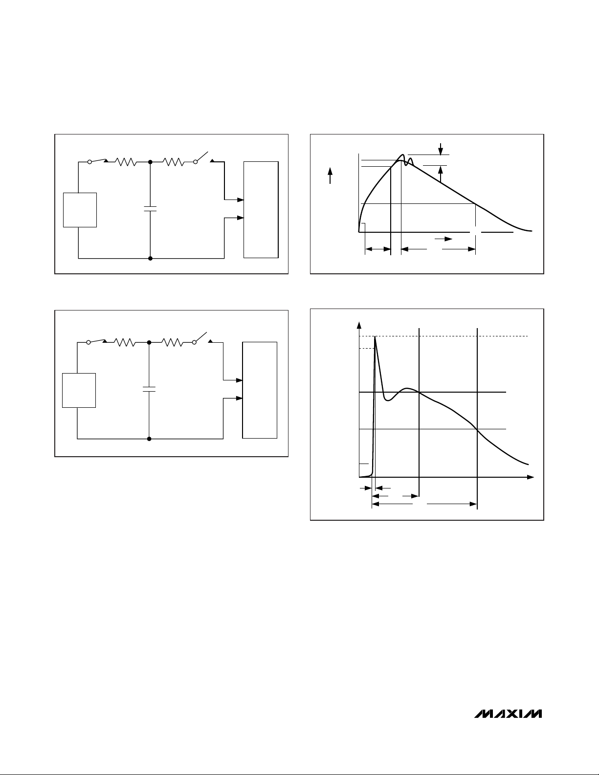
Human Body Model
Figure 11 shows the Human Body Model and Figure 12
shows the current waveform it generates when discharged into a low impedance. This model consists of
a 100pF capacitor charged to the ESD voltage of interest, which is then discharged into the test device
through a 1.5kΩ resistor.
IEC 1000-4-2
The IEC 1000-4-2 standard covers ESD testing and
performance of finished equipment; it does not specifically refer to integrated circuits. The major difference
between tests done using the Human Body Model and
IEC 1000-4-2 is a higher peak current in IEC 1000-4-2,
because series resistance is lower in the IEC 1000-4-2
model. Hence, the ESD withstand voltage measured to
IEC 1000-4-2 is generally lower than that measured
using the Human Body Model. Figure 13 shows the IEC
1000-4-2 model. The Air-Gap Discharge test involves
approaching the device with a charged probe. The
Contact Discharge method connects the probe to the
device before the probe is energized. Figure 14 shows
the IEC 1000-4-2 current waveform.
Machine Model
The Machine Model for ESD tests all pins using a
200pF storage capacitor and zero discharge resistance. Its objective is to emulate the stress caused by
contact that occurs with handling and assembly during
manufacturing. All pins require this protection during
manufacturing. The Machine Model is less relevant to
I/O ports after PC board assembly.
Layout Considerations
The MAX3353E high oscillator frequency makes proper
layout important to ensure stability and maintain the
output voltage under all loads. For best performance,
minimize the distance between the capacitors and the
MAX3353E.
UCSP Reliability
For the latest application details on UCSP construction,
dimensions, tape-carrier information, printed circuit board
techniques, bump-pad layout, and recommended reflow
temperature profile as well as the latest information on
reliability testing results, refer to Maxim Application Note:
UCSP – A Wafer-Level Chip Scale Package available on
Maxim’s website at www.maxim-ic.com/ucsp.
MAX3353E
USB On-the-Go Charge Pump with Switchable
Pullup/Pulldown Resistors
______________________________________________________________________________________ 17
Page 18
MAX3353E
USB On-the-Go Charge Pump with Switchable
Pullup/Pulldown Resistors
18 ______________________________________________________________________________________
Figure 11. Human Body ESD Test Models
Figure 12. Human Body Model Current Waveform
Figure 13. IEC 1000-4-2 ESD Test Model
Figure 14. IEC 1000-4-2 Current Waveform
R
HIGH-
VOLTAGE
DC
SOURCE
C
1MΩ
CHARGE-CURRENT-
LIMIT RESISTOR
C
100pF
s
1.5kΩ
DISCHARGE
RESISTANCE
STORAGE
CAPACITOR
R
C
HIGH-
VOLTAGE
DC
SOURCE
50Ω to 100Ω
CHARGE-CURRENT-
LIMIT RESISTOR
C
150pF
s
330Ω
DISCHARGE
RESISTANCE
STORAGE
CAPACITOR
R
D
I
r
PEAK-TO-PEAK RINGING
(NOT DRAWN TO SCALE)
DEVICE
UNDER
TEST
AMPERES
IP 100%
90%
36.8%
10%
0
0
t
RL
TIME
t
DL
CURRENT WAVEFORM
R
D
DEVICE
UNDER
TEST
PEAK
I
I
100%
90%
10%
= 0.7ns TO 1ns
t
r
30ns
60ns
t
Page 19

MAX3353E
USB On-the-Go Charge Pump with Switchable
Pullup/Pulldown Resistors
______________________________________________________________________________________ 19
Pin Configurations
Typical Applications Circuit
Chip Information
TRANSISTOR COUNT: 9394
PROCESS: BiCMOS
TOP VIEW
V
1
CC
V
2
L
SDA
3
4
MAX3353EEUE
SCL
5
INT
6
ID_OUT
7
V
8
TRM
TSSOP
ID_IN GND C- C+
D+
A
D-
B
C
V
TRM
D
ID_OUT
12345
MAX3353EEBP
ADD
INT SCL SDA V
UCSP
16
V
BUS
15
C+
14
C-
13
GNDADD
N.C.
12
ID_IN
11
10
D+
D-
9
V
BUS
V
CC
0.1μF
μP
D-
PULLUP
RESISTORS
4.7kΩ 4.7kΩ
D+
VLV
V
SDA
SCL
INT
ID_OUT
ADD
GND
L
MAX3353E
L
V
CC
TRM
0.1μF
0.1μF
V
V
CC
TRM
C1+
C1-
V
BUS
ID_IN
C
FLYING
0.1μF
C
VBUS
1μF
D+
D-
OTG CONNECTOR
V
ID
D+
DGND
BUS
Page 20
MAX3353E
USB On-the-Go Charge Pump with Switchable
Pullup/Pulldown Resistors
20 ______________________________________________________________________________________
Package Information
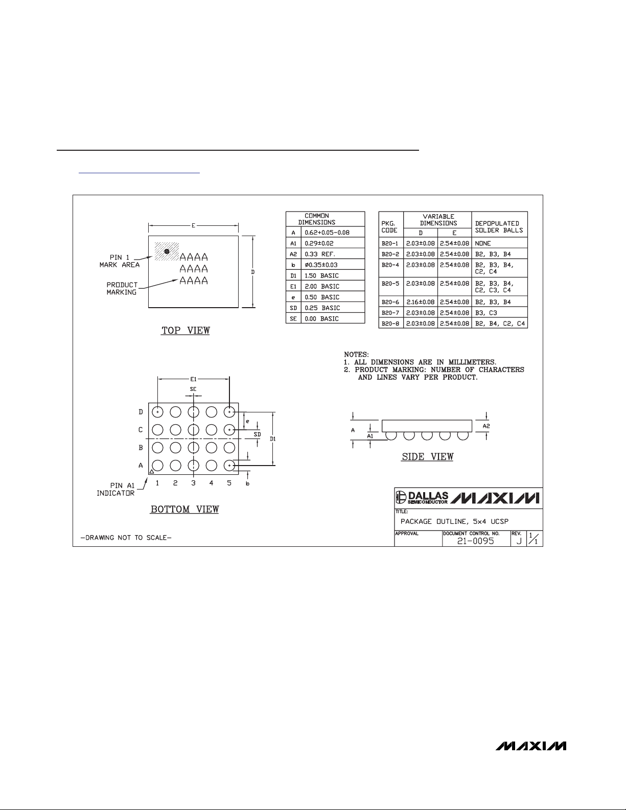
(The package drawing(s) in this data sheet may not reflect the most current specifications. For the latest package outline information,
go to www.maxim-ic.com/packages
.)
5x4 UCSP.EPS
Page 21
MAX3353E
USB On-the-Go Charge Pump with Switchable
Pullup/Pulldown Resistors
Maxim cannot assume responsibility for use of any circuitry other than circuitry entirely embodied in a Maxim product. No circuit patent licenses are
implied. Maxim reserves the right to change the circuitry and specifications without notice at any time.
Maxim Integrated Products, 120 San Gabriel Drive, Sunnyvale, CA 94086 408-737-7600 ____________________ 21
© 2003 Maxim Integrated Products Printed USA is a registered trademark of Maxim Integrated Products.
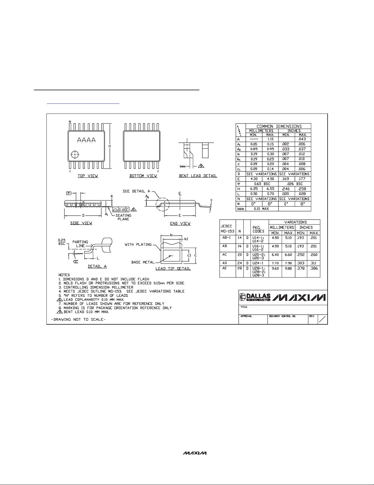
Package Information (continued)
(The package drawing(s) in this data sheet may not reflect the most current specifications. For the latest package outline information,
go to www.maxim-ic.com/packages
.)
TSSOP4.40mm.EPS
PACKAGE OUTLINE, TSSOP 4.40mm BODY
21-0066
1
1
I
 Loading...