

Page 1
General Description
The MAX3346E bidirectional transceiver converts logiclevel signals to USB signals, and USB signals to logiclevel signals. The MAX3346E includes the 1.5kΩ USB
pullup resistor internally, and supports both full-speed
(12Mbps) and low-speed (1.5Mbps) USB operation.
The device has built-in ±15kV ESD protection circuitry
to guard the USB I/O pins, D+ and D-.
The MAX3346E operates with VLvoltages as low as
1.65V, ensuring compatibility with low-voltage ASICs.
The device features a logic-selectable suspend mode
that lowers current draw to less than 40µA. The
MAX3346E has an enumerate function that allows
devices to logically disconnect while plugged in. The
MAX3346E is fully compliant with USB specification 1.1,
and the full-speed and low-speed operation under USB
specification 2.0.
The MAX3346E is available in the miniature 4 x 4 chipscale package (UCSPTM), as well as the small 14-pin
TSSOP, and is rated for the -40°C to +85°C extended
temperature range.
Applications
Cell Phones
PC Peripherals
Data Cradles
PDAs
MP3 Players
Features
♦ ±15kV ESD Protection on D+ and D-
♦ Internal Linear Regulator Allows Direct Powering
from the USB Cable
♦ Internal 1.5kΩ Pullup Resistor for Low/Full-Speed
Operation
♦ Supports Low-Speed and Full-Speed USB
Communications
♦ Complies with USB Specification Revision 1.1 and
2.0 (Low Speed and Full Speed)
♦ Three-State Outputs
♦ Enumerate Input—Allows USB Connection
through Software
♦ No Power-Supply Sequencing Required
♦ Operates with VLof 1.65V to 3.6V, Ensuring
Compatibility with Low-Voltage ASICs
♦ Available in Miniature Chip-Scale Package
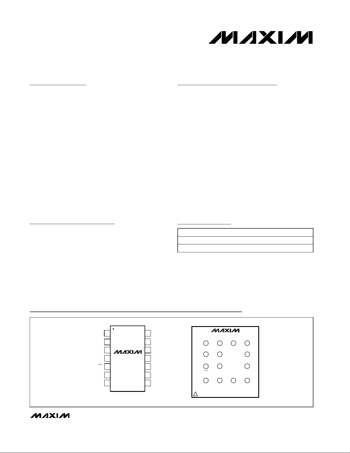
MAX3346E
±15kV ESD-Protected USB Transceiver
in UCSP
________________________________________________________________ Maxim Integrated Products 1
14
13
12
11
10
9
8
1
2
3
4
5
6
7
V
L
VTRM
D+
D-VM
MODE
VP
RCV
TOP VIEW
MAX3346E
GND
V
CC
SPEEDSUSP
ENUM
OE
TSSOP
BOTTOM VIEW
UCSP
V
CC
V
L
GND
VTRM
D+
D-
SPEED
MODE
RCV
SUSP
VM
VP
ENUM
OE
MAX3346E
A
B
C
D
1234
Pin Configurations
Ordering Information
19-3172; Rev 0; 2/04
For pricing, delivery, and ordering information, please contact Maxim/Dallas Direct! at
1-888-629-4642, or visit Maxim’s website at www.maxim-ic.com.
PART
TEMP RANGE
PIN-PACKAGE
MAX3346EEUD
14 TSSOP
MAX3346EEBE-T
4 x 4 UCSP
UCSP is trademark of Maxim Integrated Products, Inc.
-40°C to +85°C
-40°C to +85°C
Page 2
MAX3346E
±15kV ESD-Protected USB Transceiver
in UCSP
2 _______________________________________________________________________________________
ABSOLUTE MAXIMUM RATINGS
Stresses beyond those listed under “Absolute Maximum Ratings” may cause permanent damage to the device. These are stress ratings only, and functional
operation of the device at these or any other conditions beyond those indicated in the operational sections of the specifications is not implied. Exposure to
absolute maximum rating conditions for extended periods may affect device reliability.
Supply Voltage (VCC) ...............................................-0.3V to +6V
Output of Internal Regulator (VTRM)..........-0.3V to (V
CC
+ 0.3V)
Input Voltage (D+, D-)..............................................-0.3V to +6V
System Supply Voltage (V
L
) .....................................-0.3V to +6V
RCV, SUSP, VM, VP, MODE,
OE, SPEED, ENUM ....................................-0.3V to (VL+ 0.3V)
Short-Circuit Current (D+, D-)
to V
CC
or GND (Note 1) ..........................................Continuous
Maximum Continuous Current (all other pins)..................±15mA
Continuous Power Dissipation (TA= +70°C)
4 x 4 UCSP (derate 7.4mW/°C above +70°C).....589mW [B16-2]
14-Pin TSSOP (derate 9.1mW/°C above +70°C)..727mW [U14-1]
Operating Temperature Range ...........................-40°C to +85°C
Junction Temperature......................................................+150°C
Storage Temperature Range .............................-65°C to +150°C
Lead Temperature (soldering, 10s) .................................+300°C
Bump Temperature (soldering) Reflow............................+235°C
PARAMETER
CONDITIONS
UNITS
SUPPLY INPUTS (VCC, VTRM, VL)
Regulated Supply Voltage
V
VTRM
Internal regulator 3.0 3.3 3.6 V
VL Input Range
V
VCC Input Range 4.0 5.5 V
Operating VCC Supply Current I
VCC
Full-speed transmitting/receiving at
12Mbps, C
L
= 50pF on D+ and D-
8mA
Operating VL Supply Current I
VL
6mA
Full-speed idle: V
D+
> 2.7V, VD- < 0.3V
450
Full-Speed Idle and SE0 Supply
Current
)
SE0: VD+ < 0.3V, VD- < 0.3V
500
µA
Static VL Supply Current
)
Full-speed idle, SE0, or suspend mode 5 µA
Suspend Supply Current
)
SUSP = OE = high 40 µA
Disable-Mode Supply Current
)
VL = GND or open 20 µA
D+/D- Disable-Mode
Load Current
I
D_(DIS)
VL = GND or open, V
D_
= 0 or +5.5V 5 µA
Sharing-Mode VL Supply
Current
)
VCC = GND or open, OE = low,
SUSP = high
20 µA
D+/D- Sharing-Mode
Load Current
)
VCC = GND or open, V
D_
= 0 or +5.5V 20 µA
LINEAR REGULATOR
External Capacitor C
OUT
Compensation of linear regulator 1 µF
(All voltages referenced to GND, unless otherwise noted.)
Note 1: External 23.7Ω resistors connected to D+ and D-.
ELECTRICAL CHARACTERISTICS
(VCC= +4V to +5.5V, GND = 0, VTRM = +3.0V to +3.6V, VL= +1.65V to +3.6V, TA= T
MIN
to T
MAX
, unless otherwise noted. Typical
values are at V
CC
= +5V, VL= +2.5V, TA= +25°C.) (Note 2)
SYMBOL
MIN TYP MAX
1.65 3.60
Full-speed transmitting/receiving at 12Mbps
I
VCC(IDLE
I
VL(STATIC
I
VCC(SUSP
I
VCC(DIS
I
VL(SHARING
I
D_(SHARING
340
390
Page 3
PARAMETER
SYMBOL
CONDITIONS
MIN
TYP
MAX
UNITS
ESD PROTECTION (D+, D-)
Human Body Model
kV
IEC 1000-4-2 Air-Gap Discharge
kV
IEC 1000-4-2 Contact Discharge
±8kV
LOGIC-SIDE I/O
Input High Voltage V
IH
VP, VM, SUSP, SPEED, OE, MODE, ENUM (2/3) x V
L
V
Input Low Voltage V
IL
VP, VM, SUSP, SPEED, OE, MODE, ENUM 0.4 V
Output High Voltage V
OH
I
SOURCE
= +2mA, RCV, VP, VM VL - 0.4 V
Output Low Voltage V
OL
I
SINK
= -2mA, RCV, VP, VM 0.4 V
Input Leakage Current VP, VM, SUSP, ENUM, OE, MODE = 0 or V
L
±1µA
USB-SIDE I/O
Output-Voltage Low V
OLD
RL = 1.5kΩ from D+ or D- to 3.6V 0.3 V
Output-Voltage High V
OHD
RL = 15kΩ from D+ and D- to GND 2.8 3.6 V
Input Impedance Z
IN
VD_ = 0 or +3.6V, ENUM = 0,
three-state driver
1MΩ
Single-Ended Input-Voltage High
V
IH
2.0 V
Single-Ended Input-Voltage Low
V
IL
0.8 V
D+, D- Receiver Hysteresis
mV
D r i ver Outp ut Im p ed ance R
OUT
4.6
Ω
Internal Resistor
1.5
kΩ
Input Common-Mode Voltage
0.8 2.5 V
Differential Input Sensitivity
mV
MAX3346E
±15kV ESD-Protected USB Transceiver
in UCSP
_______________________________________________________________________________________ 3
ELECTRICAL CHARACTERISTICS (continued)
(VCC= +4V to +5.5V, GND = 0, VTRM = +3.0V to +3.6V, VL= +1.65V to +3.6V, TA= T
MIN
to T
MAX
, unless otherwise noted. Typical
values are at V
CC
= +5V, VL= +2.5V, TA= +25°C.) (Note 2)
TIMING CHARACTERISTICS
(VCC= +4V to +5.5V, GND = 0, VTRM = +3.0V to +3.6V, VL= +1.65V to +3.6V, TA= T
MIN
to T
MAX
, unless otherwise noted. Typical
values are at V
CC
= +5V, VL= +2.5V, TA= +25°C.) (Note 2)
PARAMETER
CONDITIONS
UNITS
SPEED INDEPENDENT TIMING CHARACTERISTICS
OE to VP/VM Three-State Delay
Disable Time
t
PVZ
Figures 1a and 4a 20 ns
OE to VP/VM Delay
Enable Time
t
PZV
Figures 1a and 4a 25 ns
D+/D- to RCV Propagation Delay
t
PLH
CL = 25pF, Figures 4b and 5 18 ns
D+/D- to RCV Propagation Delay
t
PHL
CL = 25pF, Figures 4b and 5 18 ns
R
PULLUP
±15
±10
200
1.410
16.0
1.540
SYMBOL
200
MIN TYP MAX
Page 4
MAX3346E
±15kV ESD-Protected USB Transceiver
in UCSP
4 _______________________________________________________________________________________
TIMING CHARACTERISTICS (continued)
(VCC= +4V to +5.5V, GND = 0, VTRM = +3.0V to 3.6V, VL= +1.65V to +3.6V, TA= T
MIN
to T
MAX
, unless otherwise noted. Typical
values are at V
CC
= +5V, VL= +2.5V, TA= +25°C.) (Note 2)
PARAMETER
SYMBOL
CONDITIONS
MIN
TYP
MAX
UNITS
t
PLH
CL = 25pF, Figures 4b and 5 18
D+/D- to VP/VM Propagation
Delay
t
PHL
CL = 25pF, Figures 4b and 5 18
ns
FULL-SPEED TIMING CHARACTERISTICS
OE to Transmit Delay Enable
Time
t
PZD
(Figures 1b, 4d) 20 ns
OE to Driver Three-State Delay
Disable Time
t
PDZ
(Figures1b, 4d) 20 ns
t
PLH
(Figures 3, 4c) 18
VP/VM to D+/D- Propagation
Delay (MODE = 1)
t
PHL
(Figures 3, 4c) 18
ns
t
PHL0
CL = 50pF (Figures 2, 4c) 20
VP to D+/D- Propagation Delay
(MODE = 0)
t
PLH0
CL = 50pF (Figures 2, 4c) 20
ns
D+, D- Rise Time t
R
CL = 50pF, 10% to 90% of |VOH - VOL|4 20ns
D+, D- Fall Time t
F
CL = 50pF, 90% to 10% of |VOH - VOL|4 20ns
Rise- and Fall-Time Matching
(Note 3)
t
R/tF
CL = 50pF 90
%
Output-Signal Crossover Voltage
(Note 3)
V
CRS
CL = 50pF 1.3 2.0 V
LOW-SPEED TIMING CHARACTERISTICS
t
PLH
Figures 3 and 4c, CL = 50pF to 600pF 30
VP/VM to D+/D- Propagation
Delay (MODE = 1)
t
PHL
Figures 3 and 4c, CL = 50pF to 600pF 30
ns
t
PHL0
Figures 2 and 4c, CL = 50pF to 600pF 30
VP to D+/D- Propagation Delay
(MODE = 0)
t
PLH0
Figures 2 and 4c, CL = 50pF to 600pF 30
ns
D+/D- Rise Time t
R
CL = 50pF to 600pF 75
ns
D+/D- Fall Time t
F
CL = 50pF to 600pF 75
ns
Rise- and Fall-Time Matching tR/t
F
CL = 50pF to 600pF 80
%
Output-Signal Crossover Voltage
V
CRS
CL = 50pF to 600pF 1.3 2.0 V
Note 2: Parameters are 100% production tested at +25°C, limits over temperature are guaranteed by design.
Note 3: Guaranteed by design, not production tested.
110
250
250
250
250
300
300
125
Page 5
MAX3346E
±15kV ESD-Protected USB Transceiver
in UCSP
_______________________________________________________________________________________ 5
SINGLE-ENDED RECEIVER
PROPAGATION DELAY vs. V
L
MAX3346E toc01
VL (V)
PROPAGATION DELAY (ns)
3.33.01.8 2.1 2.4 2.7
8
9
10
11
12
13
14
15
7
1.5 3.6
TA = +85°C
TA = +25°C
TA = -40°C
SINGLE-ENDED RECEIVER
PROPAGATION DELAY vs. V
CC
MAX3346E toc02
V
CC
(V)
PROPAGATION DELAY (ns)
5.00 5.254.754.25 4.50
8
9
10
11
12
13
14
15
7
4.00 5.50
TA = +85°C
TA = +25°C
TA = -40°C
SKEW vs. V
CC
(MODE 0, FULL SPEED)
MAX3346E toc03
V
CC
(V)
SKEW (ns)
5.00 5.254.754.25 4.50
0.6
0.8
1.0
1.2
1.4
1.6
1.8
2.0
0.4
4.00 5.50
TA = +85°C
TA = +25°C
TA = -40°C
0
0.1
0.2
0.6
0.4
0.8
0.3
0.7
0.5
0.9
1.0
4.00 4.504.25 4.75 5.00 5.25 5.50
SKEW VS. V
CC
(MODE 0, LOW SPEED)
MAX3346E toc04
VCC (V)
SKEW (ns)
TA = -40°C
TA = +25°C
TA = +85°C
MAX3346E toc05
A
0
0
200ns/div
B
0
C
OE, VP, VM TIMING
A: VP, 2V/div
B: VM, 2V/div
C: OE, 5V/div
(FIGURE 4a)
MAX3346E toc06
A
0
0
200ns/div
B
0
C
OE, VP, VM TIMING
A: VP, 2V/div
B: VM, 2V/div
C: OE, 5V/div
(FIGURE 4a)
VTRM vs. V
CC
MAX3346E toc07
VCC (V)
VTRM (V)
5.255.004.754.504.25
3.1
3.2
3.3
3.4
3.5
3.0
4.00 5.50
I
VTRM
= 15mA
Typical Operating Characteristics
(VCC= +5V, VL=+3.3V, TA = +25°C, unless otherwise noted.)
Page 6
MAX3346E
±15kV ESD-Protected USB Transceiver
in UCSP
6 _______________________________________________________________________________________
RISE- AND FALL-TIME MATCHING
(LOW SPEED)
MAX3346E toc09
D+
100ns/div
0
D-
f = 750kHz
RISE- AND FALL-TIME MATCHING
(FULL SPEED)
MAX3346E toc10
D+
20ns/div
0
D-
f = 6MHz
Typical Operating Characteristics (continued)
(VCC= +5V, VL= +3.3V, TA = +25°C, unless otherwise noted.)
Pin Description
PIN
TSSOP
UCSP
NAME
INPUT/
FUNCTION
1D2RCV Output
Receiver Output. Single-ended CMOS output. RCV responds to the differential
input on D+ and D- (see Table 3).
2D1VP
Input/
Output
System-Side Data Input/Output. Drive OE high to make VP a receiver output.
Drive OE low to make VP a driver input (see Table 3).
3C2MODE Input
Mode Control Input. Selects single-ended (mode zero) or differential (mode one)
input for the system side when converting logic-level signals to USB-level
signals. If MODE is forced high, mode one is selected. If MODE is forced low,
mode zero is selected (see Table 3).
4C1VM
Input/
Output
System-Side Data Input/Output. Drive OE high to make VM a receiver output.
Drive OE low to make VM a driver input (see Table 3).
5B1OE Input
Output Enable. Drive OE high to enable the receiver. Drive OE low to enable the
driver input.
6A1ENUM Input
Enumerate Input. Drive ENUM low to disconnect the internal 1.5kΩ resistor, and
enumerate the USB. With ENUM high, the internal 1.5kΩ resistor is connected to
either D+ or D-, depending on the state of SPEED.
SUSPEND RESPONSE
A
0
B
0
A: SUSP, 2V/div
B: RCV, 2V/div
MAX3346E toc08
100ns/div
OUTPUT
Page 7

MAX3346E
±15kV ESD-Protected USB Transceiver
in UCSP
_______________________________________________________________________________________ 7
Detailed Description
The MAX3346E is a bidirectional transceiver that converts single-ended or differential logic-level signals to
differential USB signals, and converts differential USB
signals to single-ended or differential logic-level signals. The MAX3346E includes an internal 1.5kΩ pullup
resistor that can be connected to either D+ or D- for
full-speed or low-speed operation (see the Functional
Diagram). The MAX3346E can be energized without
concern about power-supply sequencing. Additionally,
the USB I/O, D+ and D-, are ESD protected to ±15kV.
The MAX3346E can get its USB-side power, VCC,
directly from the USB connection, and can operate with
system-side power, V
L
, down to 1.65V and still meet the
USB physical layer specifications. The MAX3346E supports both full-speed (12Mbps) and low-speed
(1.5Mbps), USB specification 1.1 operation.
The MAX3346E has an enumerate feature that works
when power is on. Driving ENUM low disconnects the
internal 1.5kΩ pullup resistor from both D+ and D-,
reenumerating the USB. This is useful if changes in communication protocol are required while power is applied,
and while the USB cable is connected.
PIN
TSSOP
UCSP
NAME
INPUT/
FUNCTION
7B2SUSP Input
Suspend Input. Drive SUSP low for normal operation. Force SUSP high for lowpower state. In low-power state RCV is low, D+/D- are high impedance if OE is
floating, and VP/VM are active outputs.
8A2
Input
USB Transmission Speed Select Input. If SPEED is forced high, full speed
(12Mbps) is selected and the internal 1.5kΩ pullup resistor is connected to D+.
If SPEED is forced low, low speed (1.5Mbps) is selected and the internal 1.5kΩ
pullup resistor is connected to D-.
9A3VCCPower
USB-Side Power-Supply Input. Connect V
CC
to the incoming USB power supply.
Bypass V
CC
to GND with a 1µF ceramic capacitor.
10 A4 GND Power Ground
11 B4 D-
Input/
Output
USB Differential Data Input/Output. Connect to the USB’s D- signal through a
24.3Ω ±1% resistor.
12 C4 D+
Input/
Output
USB Differential Data Input/Output. Connect to the USB’s D+ signal through a
24.3Ω ±1% resistor.
13 D4 VTRM Power
Regulated Output Voltage. 3.3V output derived from the V
CC
input. Bypass
VTRM to GND with a 1µF (or more) low-ESR capacitor, such as ceramic or
plastic film types.
14 D3 V
L
Power
System-Side Power-Supply Input. Connect to the system’s logic-level power
supply, 1.65V to 3.6V. Bypass to GND with a 0.1µF capacitor.
— B3, C3 — —
Not populated. The solder sphere is omitted from these locations (see the
Package Information).
Pin Description (continued)
SPEED
OUTPUT
Page 8

MAX3346E
±15kV ESD-Protected USB Transceiver
in UCSP
8 _______________________________________________________________________________________
Applications Information
Power-Supply Configurations
Normal Operating Mode
Connect VLand VCCto system power supplies (Table
1). Connect VLto a +1.65V to +3.6V supply. Connect
VCCto a +4.0V to +5.5V supply. Alternatively, the
MAX3346E can derive power from a single Li+ battery.
Connect the battery to VCC. VTRM remains above
+3.0V for VCCas low as +3.1V.
Additionally, the MAX3346E can derive power from a
3.3V ±10% voltage regulator. Connect VCCand VTRM
to an external +3.3V voltage regulator.
Disable Mode
Connect VCCto a system power supply and leave V
L
unconnected or connect to GND. D+ and D- enter a tristate mode and VCCconsumes less than 20µA of supply current. D+ and D- withstand external signals up to
+5.5V in disable mode (Table 2).
Sharing Mode
Connect VLto a system power supply and leave V
CC
(or VCCand V
VTRM
) unconnected or connect to GND.
D+ and D- enter a tri-state mode, allowing other circuitry to share the USB D+ and D- lines, and VLconsumes
less than 20µA of supply current. D+ and D- withstand
external signals up to +5.5V in sharing mode (Table 2).
Device Control
OE
OE controls the direction of communication through the
device. With OE low, the MAX3346E transfers data from the
system side to the USB side. With OE high, the MAX3346E
transfers data from the USB side to the system side.
ENUM
The MAX3346E allows software control of USB enumeration. USB specification 1.1 requires a 1.5kΩ pullup resistor
to D+ or D- to set the transmission speed (see the SPEED
section). Enumerating the USB requires removing the 1.5kΩ
resistor from the circuit, and is accomplished with the
MAX3346E by driving ENUM low. With ENUM high, the voltage at SPEED determines how the internal resistor is connected (see the Functional Diagram).
MODE
MODE is a control input that selects whether differential
or single-ended logic signals are recognized by the
system side of the MAX3346E (Table 3).
If MODE is forced high, differential input is selected. With
differential input selected, outputs D+ and D- follow the
differential inputs at VP and VM. If VP and VM are both
forced low, an SE0 condition is forced on the USB.
Drive MODE and VM low for single-ended input mode.
With single-ended input selected, the differential signal on D+ and D- is controlled by VP. If VM is high
when MODE is low, D- and D+ are both low, forcing
an SE0 condition.
VCC (V) VTRM (V) VL (V) CONFIGURATION NOTES
+4.0 to +5.5 +3.3 Output +1.65 to +3.6 Normal mode —
+3.1 to +4.5 +3.3 Output +1.65 to +3.6 Battery supply —
+3.0 to +3.6 +3.0 to +3.6 Input +1.65 to +3.6
—
GND or floating Output +1.65 to +3.6 Sharing mode Table 2
+3.0 to +5.5 Output GND or floating Disable mode Table 2
Table 1. Power-Supply Configurations
INPUTS/OUTPUTS DISABLE MODE SHARING MODE
VCC/VTRM
• +5V input/+3.3V output
• +3.3V input/+3.3V output
• +3.7V input/+3.3V output
Floating or connected to GND
V
L
Floating or connected to GND +1.65V to +3.6V input
D+ and D- High impedance High impedance
SPEED, SUSP, OE, ENUM High impedance High impedance
Table 2. Disable-Mode and Sharing-Mode Configurations
Voltage regulator supply
Page 9

MAX3346E
±15kV ESD-Protected USB Transceiver
in UCSP
_______________________________________________________________________________________ 9
SUSP
SUSP, or suspend, is a control input. When SUSP is
forced high the MAX3346E enters a low-power state. In
this state, the quiescent supply current into VCCis less
than 40µA. In this mode, RCV is forced low, and D+ and
D- are high-impedance inputs (Table 3d).
In suspend mode, data can only be transmitted with
full-speed slope control.
SPEED
SPEED is a control input that selects between low-speed
(1.5Mbps) and full-speed (12Mbps) USB transmission.
Internally, it selects whether the 1.5kΩ pullup resistor is
connected to D+ (full-speed) or D- (low-speed)
(Functional Diagram). Force SPEED high to select full
speed, or force SPEED low to select low speed.
VTRM
VTRM is the 3.3V output of the internal linear voltage
regulator. The regulator is used to power the internal
portions of the USB side of the MAX3346E. The VTRM
regulator’s supply input is V
CC
. Connect a 1.0µF (or
greater) ceramic or plastic capacitor from VTRM to
GND, as close to VTRM as possible. Do not use VTRM
to provide power to external circuitry.
D+ and D-
D+ and D- are the transceiver I/O connections, and are
ESD protected to ±15kV using the Human Body Model,
making the MAX3346E ideal for applications where a
robust transmitter is required.
V
CC
Bypass VCCto GND with a 1µF capacitor. Place the
1µF capacitor as close as possible to the MAX3346E.
Figure 1b. Enable and Disable Timing, Transmitter
Figure 1a. Enable and Disable Timing, Receiver
D+/D-
t
PDZ
t
PZD
V
OHD
- 0.3V
V
OLD
+ 0.3V
V
L
0V
VL/2
OE
Figure 2. Mode 0 Timing
t
PLH1
V
L
0V
0V
VTRM
VL/2
D+
VP
VM
D-
V
L
0V
t
PHL1
VL/2
t
PLH1
t
PHL1
VL/2
Figure 3. Mode 1 Timing
VP/VM
V
OH
- 0.3V
t
PZV
t
PVZ
VOL + 0.3V
V
L
0V
VL/2
OE
Timing Diagrams
V
L
VPO
0V
VTRM
0V
VL/2
t
PHLO
t
PLHO
D+
D-
Page 10

MAX3346E
±15kV ESD-Protected USB Transceiver
in UCSP
10 ______________________________________________________________________________________
(a) LOAD FOR ENABLE AND DISABLE TIME, VP/VM.
(b) LOAD FOR VP, VM AND RCV.
(c) LOAD FOR D+/D-.
(d) LOAD FOR ENABLE AND DISABLE TIME, D+/D-.
VP or VM
GND
or V
CC
TEST POINT
200
Ω
25pF
+
-
MAX3346E
VM or VP or RCV
25pF
MAX3346E
TEST POINT
D+ or D-
23.7
Ω
C
L
15k
Ω
1.5k
Ω
3.3V
MAX3346E
TEST POINT
D+ or D-
200
Ω
23.7
Ω
MAX3346E
50pF
GND
or V
CC
+
-
TEST POINT
Figure 4. Test Circuits
t
PHL
t
PLH
t
PHL
t
PLH
t
PLH
t
PHL
D+
D-
RCV
VP
VM
D+/D- RISE/FALL TIMES ≤ 8ns, V
L
= 1.65V, 2.5V, 3.3V
3V
0V
V
L
VL/2
V
L
/2
V
L
/2
0V
V
L
0V
V
L
0V
Figure 5. D+/D- to RCV, VP, VM Propagation Delays
Page 11

MAX3346E
±15kV ESD-Protected USB Transceiver
in UCSP
______________________________________________________________________________________ 11
OE = 0 (TRANSMIT)
INPUT OUTPUT
VP VM D+ D- RCV
RESULT
0000RCV* SE0
01010Logic 0
10101Logic 1
1111XUndefined
Table 3b. Truth Table, Transmit (MODE = 1)
OE = 1 (RECEIVE)
INPUT OUTPUT
D+ D- VP VM RCV
RESULT
0000RCV* SE0
01010Logic 0
10101Logic 1
1111XUndefined
Table 3c. Truth Table, Receive
SUSP
OE D+/D- RCV VP/VM FUNCTION
000Driving Active High-Z Normal driving
001High-Z Active Active Normal receiving, R
PULLUP
disconnected
010Driving Active High-Z Normal driving
011High-Z Active Active Normal receiving, R
PULLUP
connected
100 or 1 High-Z 0 Active Suspend mode, R
PULLUP
disconnected
110 or 1 High-Z 0 Active Suspend mode, R
PULLUP
connected
Table 3d. Function Select
OE = 0 (TRANSMIT)
INPUT OUTPUT
VP VM D+ D- RCV
RESULT
00010Logic 0
0100RCV* SE0
10101Logic 1
1100XSE0
Table 3a. Truth Table, Transmit (MODE = 0)
*RCV denotes the signal level on output RCV just before SE0 state occurs. This level is stable during the SE0 period.
*RCV denotes the signal level on output RCV just before SE0 state occurs. This level is stable during the SE0 period.
*RCV denotes the signal level on output RCV just before SE0 state occurs. This level is stable during the SE0 period.
ENUMERATE
Page 12

MAX3346E
±15kV ESD-Protected USB Transceiver
in UCSP
12 ______________________________________________________________________________________
External Components
External Resistors
Two external resistors are required for USB connection,
each of them from 23.7Ω ±1% to 27.4Ω ±1%, 1/2W (or
greater). Place one resistor in series between D+ of the
MAX3346E and D+ of the USB connector. Place the
other resistor in series between D- of the MAX3346E
and D- of the USB connector. The Typical Operating
Circuit shows these connections.
External Capacitors
Four external capacitors are recommended for proper
operation. Use a 0.1µF ceramic for decoupling VL, a
1µF ceramic capacitor for decoupling VCC, and a 1.0µF
(or greater) ceramic or plastic filter capacitor on VTRM.
Return all capacitors to GND.
Receiving Data from the USB
Data received from the USB are output to VP/VM and
RCV in either of two ways, differentially or single ended.
To receive data from the USB, force OE high, and force
SUSP low. Differential data arriving at D+/D- appears
as differential logic signals at VP/VM, and as a singleended logic signal at RCV. If both D+ and D- are low,
then VP and VM are low, signaling an SE0 condition on
the bus; RCV retains the last state before SE0 (see
Table 3).
Transmitting Data to the USB
The MAX3346E outputs data to the USB differentially on
D+ and D-. The logic driving the signals may be either
differential or single ended. For sending differential
logic, force MODE high, force OE and SUSP low, and
apply data to VP and VM. If sending single-ended
logic, force MODE, SUSP, OE, and VM low, and apply
data to VP. With VP low, D+ is low and D- high, resulting in a logic 0 state. With VP high, D+ is high and Dlow, resulting in a logic 1 state (see Table 3).
ESD protection
To protect the MAX3346E against ESD, D+ and D- have
extra protection against static electricity to protect the
device up to ±15kV. The ESD structures withstand high
ESD in all states; normal operation, suspend, and powered down. For the 15kV ESD structures to work correctly, a 1µF or greater capacitor must be connected
from VTRM to GND.
ESD protection can be tested in various ways; the D+
and D- input/output pins are characterized for protection
to the following limits:
1) ±15kV using the Human Body Model.
2) ±8kV using the Contact Discharge method specified
in IEC 1000-4-2.
3) ±10kV using the IEC 1000-4-2 Air-Gap method.
ESD Test Conditions
ESD performance depends on a variety of conditions.
Contact Maxim for a reliability report that documents
test setup, test methodology, and test results.
Human Body Model
Figure 6a shows the Human Body Model, and Figure 6b
shows the current waveform it generates when discharged into a low impedance. This model consists of a
100pF capacitor charged to the ESD voltage of interest,
which is then discharged into the test device through a
1.5kΩ resistor.
CHARGE-CURRENT
LIMIT RESISTOR
DISCHARGE
RESISTANCE
STORAGE
CAPACITOR
C
s
100pF
R
C
1M
Ω
R
D
1500
Ω
HIGH-
VOLTAGE
DC
SOURCE
DEVICE
UNDER
TEST
Figure 6a. Human Body ESD Test Models
IP 100%
90%
36.8%
t
RL
TIME
t
DL
CURRENT WAVEFORM
PEAK-TO-PEAK RINGING
(NOT DRAWN TO SCALE)
I
r
10%
0
0
AMPERES
Figure 6b. Human Body Model Current Waveform
Page 13

MAX3346E
±15kV ESD-Protected USB Transceiver
in UCSP
______________________________________________________________________________________ 1313 ___________________________________________________________________________________________________
IEC 1000-4-2
The IEC 1000-4-2 standard covers ESD testing and
performance of finished equipment; it does not specifically refer to integrated circuits. The MAX3346E helps
to design equipment that meets Level 2 of IEC 1000-42, without the need for additional ESD-protection components.
The major difference between tests done using the
Human Body Model and IEC 1000-4-2 is a higher peak
current in IEC 1000-4-2, because series resistance is
lower in the IEC 1000-4-2 model. Hence, the ESD withstand voltage measured to IEC 1000-4-2 is generally
lower than that measured using the Human Body Model.
Figure 7a shows the IEC 1000-4-2 model.
The Air-Gap Discharge test involves approaching the
device with a charged probe. The Contact Discharge
method connects the probe to the device before the
probe is energized.
Machine Model
The Machine Model for ESD tests all pins using a 200pF
storage capacitor and zero discharge resistance. Its
objective is to emulate the stress caused by contact that
occurs with handling and assembly during manufacturing. Of course, all pins require this protection during
manufacturing, not just USB inputs and outputs.
Therefore, after PC board assembly, the Machine Model
is less relevant to I/O ports.
UCSP Applications Information
For the latest application details on UCSP construction,
dimensions, tape carrier information, printed circuit board
techniques, bump-pad layout, and recommended reflow
temperature profile as well as the latest information on
reliability testing results, go to the Maxim website at
www.maxim-ic.com/ucsp for the Application Note,
“UCSP—A Wafer-Level Chip-Scale Package.”
CHARGE-CURRENT
LIMIT RESISTOR
DISCHARGE
RESISTANCE
STORAGE
CAPACITOR
C
s
150pF
R
C
50MΩ to 100M
Ω
R
D
330
Ω
HIGH-
VOLTAGE
DC
SOURCE
DEVICE
UNDER
TEST
Figure 7a. IEC 1000-4-2 ESD Test Model
Page 14

MAX3346E
±15kV ESD-Protected USB Transceiver
in UCSP
14 ______________________________________________________________________________________
23.7Ω
±1%
23.7Ω
±1%
1.0µF
CERAMIC
USB CABLE
15kΩ 15kΩ
GND
D-
D+
USB POWER
PC
MAX3346E
GND
D-
D+
V
CC
SPEED
SUSP
ENUM
RCV
VM
VP
V
L
MODE
1.0µF
CERAMIC
ASIC
0.1µF
CERAMIC
SYSTEM
POWER
VTRM
OE
Typical Operating Circuit
Page 15

MAX3346E
±15kV ESD-Protected USB Transceiver
in UCSP
______________________________________________________________________________________ 15
LINEAR
REGULATOR
INTERNAL
POWER
1.5kΩ
LEVEL SHIFTER
AND
CONTROL LOGIC
GND
VM
VP
RCV
SUSP
MODE
ENUM
V
L
SPEED
V
CC
VTRM
D+
D-
MAX3346E
OE
Functional Diagram
Chip Information
TRANSISTOR COUNT: 2162
PROCESS: BiCMOS
Page 16

MAX3346E
±15kV ESD-Protected USB Transceiver
in UCSP
16 ______________________________________________________________________________________
TSSOP4.40mm.EPS
Package Information
(The package drawing(s) in this data sheet may not reflect the most current specifications. For the latest package outline information,
go to www.maxim-ic.com/packages
.)
Page 17

MAX3346E
±15kV ESD-Protected USB Transceiver
in UCSP
Maxim cannot assume responsibility for use of any circuitry other than circuitry entirely embodied in a Maxim product. No circuit patent licenses are
implied. Maxim reserves the right to change the circuitry and specifications without notice at any time.
Maxim Integrated Products, 120 San Gabriel Drive, Sunnyvale, CA 94086 408-737-7600 ____________________ 17
© 2004 Maxim Integrated Products Printed USA is a registered trademark of Maxim Integrated Products.
Package Information (continued)
(The package drawing(s) in this data sheet may not reflect the most current specifications. For the latest package outline information,
go to www.maxim-ic.com/packages
.)
16L,UCSP.EPS
PACKAGE OUTLINE, 4x4 UCSP
21-0101
1
H
1
 Loading...