

Page 1
现货库存、技术资料、百科信息、热点资讯,精彩尽在鼎好!
General Description
The MAX3341E USB level translator converts logic-level
signals to USB signals, and USB signals to logic-level
signals. An internal 1.5kΩ USB termination resistor supports full-speed (12Mbps) USB operation. The
MAX3341E provides built-in ±15kV ESD-protection circuitry on the USB I/O pins, D+ and D-, and VCC.
The MAX3341E operates with logic supply voltages as
low as 1.8V, ensuring compatibility with low-voltage
ASICs. The suspend mode lowers supply current to
less than 50µA. A unique enumerate feature allows
changes in USB communication protocol while power is
applied. The MAX3341E is fully compliant with USB
specification 1.1, and full-speed operation under USB
specification 2.0.
The MAX3341E has a USB detect that monitors the
USB bus for insertion and signals this event.
The MAX3341E is available in the miniature 4 ✕4
UCSP™, as well as the small 16-pin TSSOP, and is
specified over the extended temperature range, -40°C
to +85°C.
Applications
Cell Phones
PC Peripherals
Information Appliances
Data Cradles
PDAs
MP3 Players
Digital Cameras
Features
♦ ±15kV ESD Protection On D+ and D-
♦ Complies with USB Standard 1.1 (Full Speed 2.0)
♦ USB Skew Independent of Input Skew
♦ Separate VP and VM Inputs/Outputs
♦ V
L
Down to 1.8V Allows Connection with Low-
Voltage ASICs
♦ Reenumerate with Power Applied
♦ USB Detect Function
♦ Allows Single-Ended or Differential Logic I/O
♦ Internal Linear Regulator Allows Direct Powering
from the USB
♦ Internal Termination Resistor for Full-Speed
Operation
♦ Three-State Outputs
♦ No Power-Supply Sequencing Required
♦ Driver Active in Suspend Mode
♦ Available in Miniature Chip-Scale Package
MAX3341E
±15kV ESD-Protected USB Level Translator in
UCSP with USB Detect
________________________________________________________________ Maxim Integrated Products 1
Ordering Information
19-2321; Rev 0; 4/02
For pricing, delivery, and ordering information, please contact Maxim/Dallas Direct! at
1-888-629-4642, or visit Maxim’s website at www.maxim-ic.com.
Pin Configurations appear at end of data sheet.
UCSP is a trademark of Maxim Integrated Products, Inc.
*Future product—contact factory for availability.
**UCSP reliability is integrally linked to the user’s assembly
methods, circuit board material, and environment. See the
UCSP Reliability Notice in the UCSP Reliability section of this
data sheet for more information.
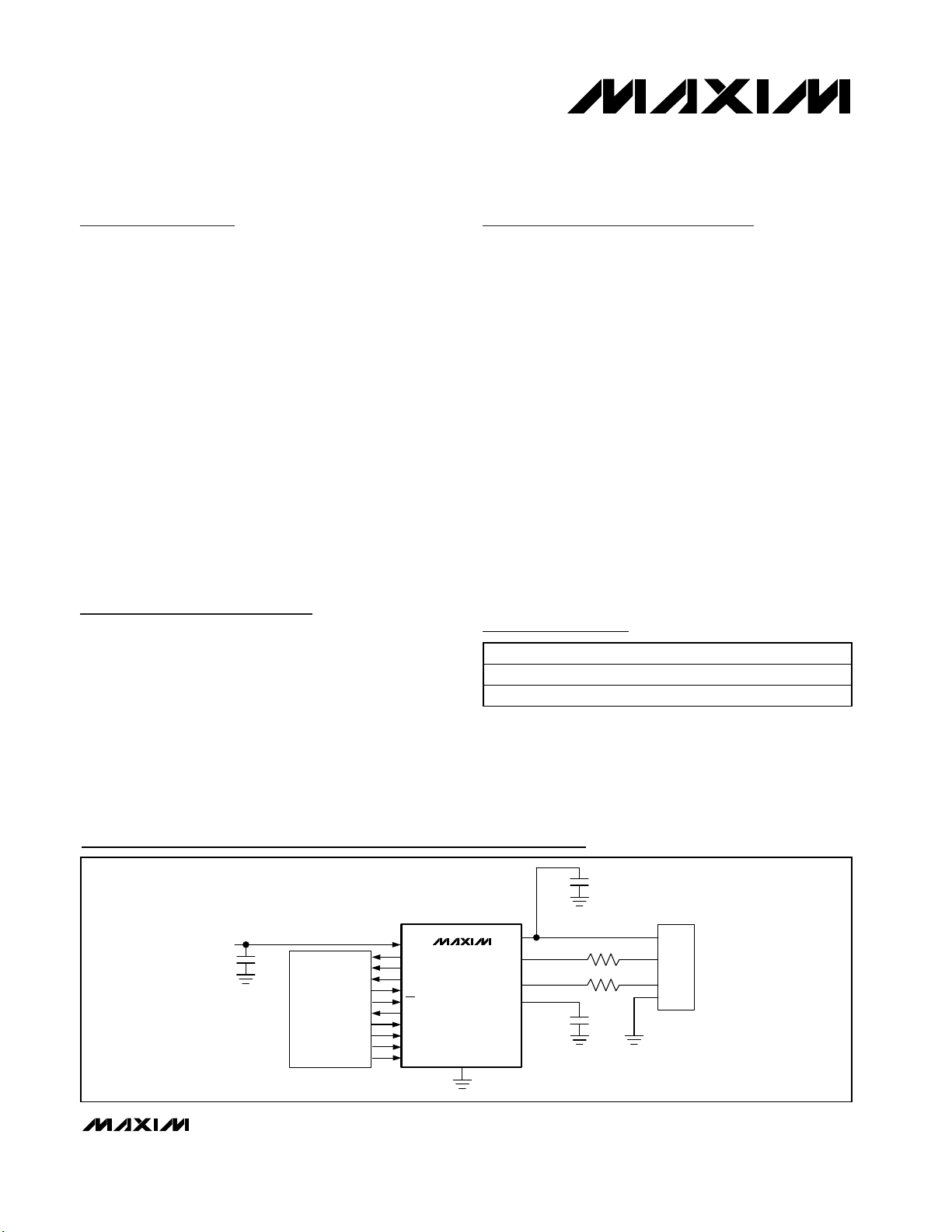
Typical Operating Circuit
PART TEMP RANGE PIN-PACKAGE
MAX3341EEUD -40°C to +85°C 16 TSSOP
MAX3341EEBE* -40°C to +85°C4 ✕ 4 UCSP**
1µF
V
SYSTEM
SUPPLY
VOLTAGE
0.1µF
SYSTEM INTERFACE
V
L
RCV
VPI
VMI
SUSPEND
OE
USB_DET
MODE
ENUMERATE
VPO
VMO
MAX3341E
GND
V
VTRM
CC
D+
D-
23.7Ω
23.7Ω
1µF
BUS
D+
D-
GND
USB
INTERFACE
CONNECTOR
Page 2
MAX3341E
±15kV ESD-Protected USB Level Translator in
UCSP with USB Detect
2 _______________________________________________________________________________________
ABSOLUTE MAXIMUM RATINGS
ELECTRICAL CHARACTERISTICS
(VCC= 4V to 5.5V bypassed with 1µF to GND, GND = 0, VL= 1.8V to 3.6V, D+ to GND = 15kΩ, D- to GND = 15kΩ, ENUM = VL,
T
A
= T
MIN
to T
MAX
, unless otherwise noted. Typical values are at VCC= 5V, VL= 2.5V, TA= +25°C.)
Stresses beyond those listed under “Absolute Maximum Ratings” may cause permanent damage to the device. These are stress ratings only, and functional
operation of the device at these or any other conditions beyond those indicated in the operational sections of the specifications is not implied. Exposure to
absolute maximum rating conditions for extended periods may affect device reliability.
)
)
Note 1: Guaranteed for VCC< +3.7V only.
Note 2: Absolute Maximum Rating for input voltage (D+, D-) with V
CC
> +3.7V is -0.3V to (VCC+0.3V).
Note 3: External 23.7Ω resistors connected to D+ and D-.
(All Voltages Refer to GND Unless Otherwise Noted.)
Supply Voltage (V
CC
) ...............................................-0.3V to +6V
Output of Internal Regulator (VTRM) (Note 1) ..........-0.3V to +6V
Input Voltage (D+, D-) (Notes 1, 2) ..........................-0.3V to +6V
System Supply Voltage (V
L
) .....................................-0.3V to +6V
RCV, SUSP, VMO, MODE, VPO, OE, VMI,
VPI, USB_DET, ENUM...................................-0.3V to (V
L
+ 0.3V)
Short-Circuit Current (D+, D-) to V
CC
or
Ground (Note 3) .........................................................Continuous
Maximum Continuous Current (all other pins) ..................±15mA
Continuous Power Dissipation (T
A
= +70°C)
16-Pin TSSOP (derate 7.1mW/°C above +70°C) .........571mW
4
✕
4 UCSP (derate 8.2 mW/°C above +70°C) ............659mW
Operating Temperature Range ...........................-40°C to +85°C
Junction Temperature......................................................+150°C
Storage Temperature Range .............................-65°C to +150°C
PARAMETER SYMBOL CONDITIONS MIN TYP MAX UNITS
USB Supply Voltage V
USB Supply Current I
VCC Supply Current ICC(< 3V) VCC < 3V 80 µA
D + /D - Leakag e C ur r ent I
VL Suspend Supply Current I
LOGIC-SIDE I/O
VL Input Range V
CC
CC
Data rate = 12Mbps, CL = 50pF (Figure 6b) 10 20 mA
SUSP = high, ENUM = low, OE = high 50
CC(SUSP
SUSP = high, OE = low 85USB SUSP Supply Current I
SUSP = high, ENUM = high, OE = high 85
(3V) VCC = 3V; D+, D- < 3.6V 10 µA
D+/D-
L(SUSP
L
SUSP = high, 0 < VCC < 5.5V 20 µA
4 5.5 V
1.8 3.6 V
µA
Input High Voltage V
Input Low Voltage V
Output Voltage High V
Output Voltage Low V
IH
IL
OH
OL
Input Leakag e C ur r ent S U SP , MOD E , E N UM , OE, VM O, V P O = 0 or V
SUSP, MODE, ENUM, OE, VMO, VPO 2/3 ✕ V
SUSP, MODE, ENUM, OE, VMO, VPO 0.4 V
VPI, VMI, RCV, USB_DET; I
VPI, VMI, RCV, USB_DET; I
= 1mA VL - 0.2 V
SOURCE
= -1mA 0.4 V
SINK
L
USB-SIDE I/O
Output Voltage Low V
Output Voltage High V
Input Impedance Z
S i ng l e- E nd ed Inp ut V ol tag e H i g hV
S i ng l e- E nd ed Inp ut V ol tag e Low V
Receiver Single-Ended
Hysteresis
Differential Input Sensitivity V
V
OL
OH
IN
IH
IL
HYS
DIFF
D+ or D- 0.3 V
D+ or D- 2.8 3.6 V
Three-state driver 1 MΩ
2.0 V
200 mV
L
±1 ±10 µA
0.8 V
200 mV
V
Page 3
MAX3341E
±15kV ESD-Protected USB Level Translator in
UCSP with USB Detect
_______________________________________________________________________________________ 3
ELECTRICAL CHARACTERISTICS (continued)
(VCC= 4V to 5.5V bypassed with 1µF to GND, GND = 0, VL= 1.8V to 3.6V, D+ to GND = 15kΩ, D- to GND = 15kΩ, ENUM = VL,
T
A
= T
MIN
to T
MAX
, unless otherwise noted. Typical values are at VCC= 5V, VL= 2.5V, TA= +25°C.)
TIMING CHARACTERISTICS
(VCC= 4V to 5.5V, GND = 0, VL= 1.8V to 3.6V, D+ to GND = 15kΩ, D- to GND = 15kΩ, ENUM = VL, TA= T
MIN
to T
MAX
, unless
otherwise noted. Typical values are at V
CC
= 5V, VL= 2.5V, TA= +25°C.) (Figures 2–6)
)
)
)
)
)
)
PARAMETER SYMBOL CONDITIONS MIN TYP MAX UNITS
Input Common-Mode Voltage
Range
Driver Output Impedance Z
Internal Resistor R
Termination Voltage VTRM 3.0 3.3 3.6 V
USB_DET Threshold
USB_DET Hysteresis V
LINEAR REGULATOR
Power-Supply Rejection Ratio PSRR f = 10kHz, C
External Capacitor C
ESD PROTECTION (VCC, D+, D-)
Human Body Model ±15 kV
IE C 1000- 4- 2 Ai r - Gap D i schar g e ±15 kV
IE C 1000- 4- 2 C ontact D i schar g e ±8 kV
V
CM
OUT
PU
V
USBLH
V
USBHL
USBHYS
OUT
Including 23.7Ω (±1%) external resistors 28.5 43.5 Ω
= 1µF, D+/D- load 30 dB
OUT
Compensation of linear regulator 1 µF
0.8 2.5 V
1.425 1.500 1.575 kΩ
4.0
3.7
25 mV
V
OE to Transmit Delay Enable
Time
OE to Driver Three-State Delay
Driver Disable Time
USB Detect Signal Delay t
TRANSMITTER
VPO/VMO to D+/D- Propagation
Delay
VPO to D+/D- Propagation
Delay
Rise Time D+/D- t
Fall Time D+/D- t
Rise- and Fall-Time Matching tR/t
Output Signal Crossover V
DIFFERENTIAL RECEIVER (Figure 6a)
D+/D- to RCV Propagation
Delay
Rise Time RCV t
Fall Time RCV t
PARAMETER SYMBOL CONDITIONS MIN TYP MAX UNITS
t
PZD
t
PDZ
DUSB
t
PLH1(drv
t
PHL1(drv
t
PLH0(drv
t
PHL0(drv
R
F
CRS
t
PLH(RCV
t
PHL(RCV
R
F
Figure 6c 15 80 ns
Figure 6c 25 ns
Figure 6b 7.5 µs
MODE = high , Figure 6c 30
MODE = high, Figure 6c 30
MODE = low, Figure 6c 35
MODE = low, Figure 6c 35
(Note 4) 90 110 %
F
420ns
420ns
1.3 2 V
30
30
15 ns
15 ns
ns
ns
ns
Page 4
MAX3341E
±15kV ESD-Protected USB Level Translator in
UCSP with USB Detect
4 _______________________________________________________________________________________
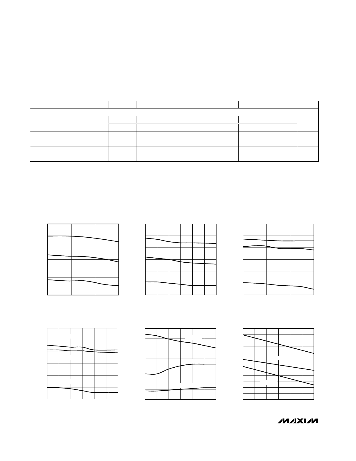
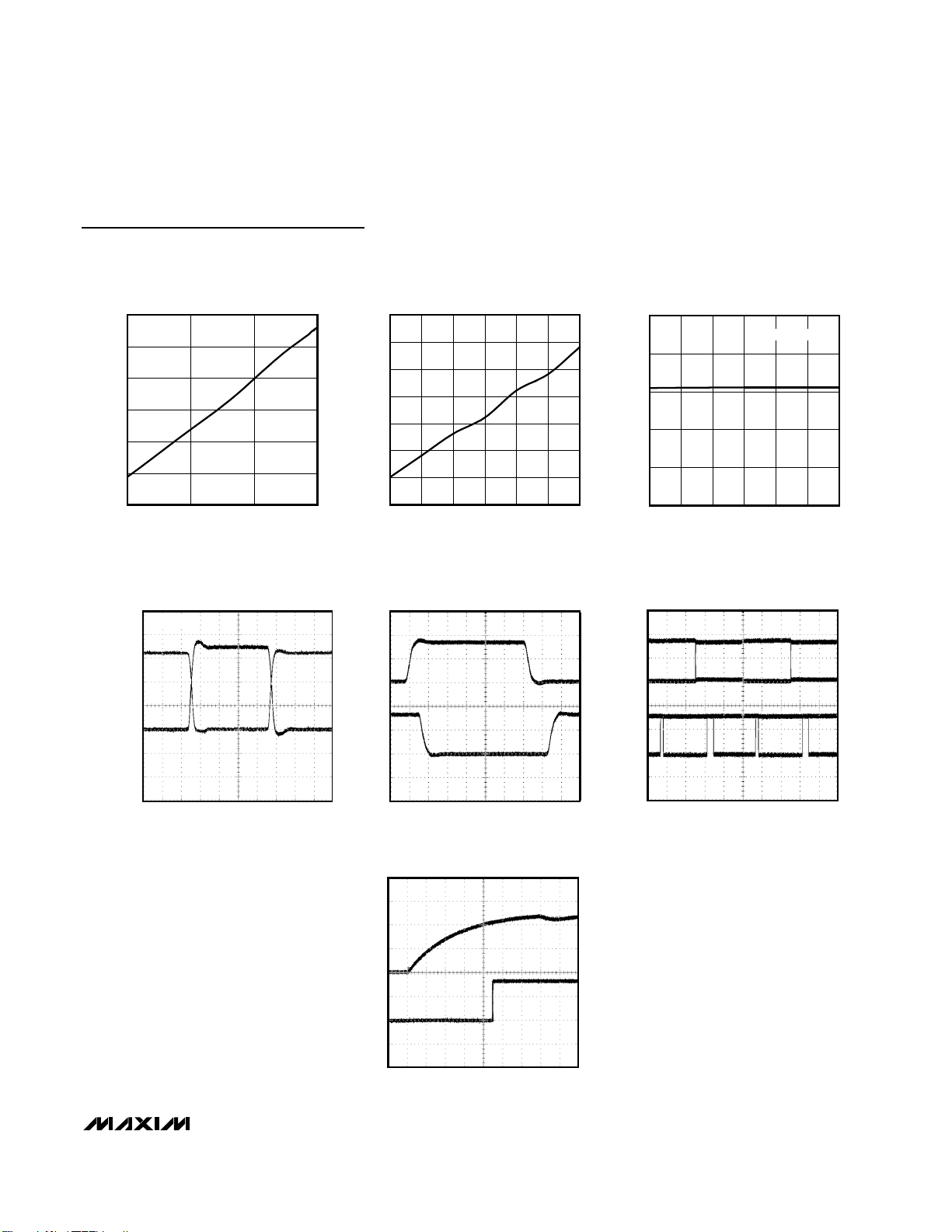
Typical Operating Characteristics
(VCC= 5V, VL= 3.3V, TA = +25°C, unless otherwise noted.)
DIFFERENTIAL RECEIVER PROPAGATION
DELAY vs. V
L
MAX3341 toc01
VL (V)
PROPAGATION DELAY (ns)
2.82.3
11
14
17
20
8
1.8 3.3
TA = +85°C
T
A
= +25°C
T
A
= -40°C
DIFFERENTIAL RECEIVER PROPAGATION
DELAY vs. V
CC
MAX3341 toc02
VCC (V)
PROPAGATION DELAY (ns)
5.255.004.754.504.25
10
12
14
16
18
20
8
4.00 5.50
TA = -40°C
TA = +25°C
TA = +85°C
SINGLE-ENDED RECEIVER PROPAGATION
DELAY vs. V
L
MAX3341 toc03
VL (V)
PROPAGATION DELAY (ns)
2.82.3
5
6
7
8
9
10
4
1.8 3.3
TA = -40°C
TA = +25°C
TA = +85°C
SINGLE-ENDED RECEIVER PROPAGATION
DELAY vs. V
CC
MAX3341 toc04
VCC (V)
PROPAGATION DELAY (ns)
5.255.004.754.504.25
5
6
7
8
9
10
4
4.00 5.50
TA = -40°C
TA = +25°C
TA = +85°C
TIME TO ENTER SUSPEND MODE
vs. V
CC
MAX3341 toc05
VCC (V)
TIME (ns)
5.255.004.754.504.25
20
25
30
35
40
45
50
15
4.00 5.50
TA = -40°C
TA = +25°C
TA = +85°C
TRANSMITTER SKEW vs. V
CC
MAX3341 toc06
VCC (V)
TRANSMITTER SKEW (ns)
5.255.004.754.504.25
1.7
1.8
1.9
2.0
2.1
2.2
2.3
2.4
2.5
2.6
2.7
2.8
1.6
4.00 5.50
TA = -40°C
TA = +25°C
TA = +85°C
TIMING CHARACTERISTICS (continued)
(VCC= 4V to 5.5V, GND = 0, VL= 1.8V to 3.6V, D+ to GND = 15kΩ, D- to GND = 15kΩ, ENUM = VL, TA= T
MIN
to T
MAX
, unless
otherwise noted. Typical values are at V
CC
= 5V, VL= 2.5V, TA= +25°C.) (Figures 2–6)
)
)
Note 4: Production tested at +25°C and +85°C only. Limit at -40°C guaranteed by correlation.
PARAMETER SYMBOL CONDITIONS MIN TYP MAX UNITS
SINGLE-ENDED RECEIVERS
D+/D- to VPI or VMI Propagation
Delay
Rise Time VPI and VMI t
Fall Time VPI and VMI t
Time to Detect Single-Ended
Zero
t
PLH(SE
t
PHL(SE
R(SE)
F(SE)
t
SE0
Figure 6a 15
Figure 6a 15
Measured from 10% to 90%,Figure 6a 15 ns
Measured from 90% to 10%, Figure 6a 15 ns
14 140 ns
ns
Page 5
MAX3341E
±15kV ESD-Protected USB Level Translator in
UCSP with USB Detect
_______________________________________________________________________________________ 5
0
Typical Operating Characteristics (continued)
(VCC= 5V, VL= 3.3V, TA = +25°C, unless otherwise noted.)
LOGIC CURRENT CONSUMPTION IN
9
8
7
(µA)
6
VL
I
5
4
3
1.8 3.3
D+
1V/div
D-
SUSPEND MODE
2.82.3
VL (V)
RISE-AND-FALL TIME MATCHING
f = 6MHz
MAX3341 toc1
MAX3341 toc07
25.5
25.0
24.5
24.0
(µA)
VCC
I
23.5
23.0
22.5
22.0
4.00 5.50
SUSP
0
2V/div
RCV
0
CURRENT CONSUMPTION IN
SUSPEND MODE
5.255.004.754.504.25
VCC (V)
SUSPEND RESPONSE
MAX3341 toc11
MAX3341 toc08
3.5
VTRM vs. V
3.4
3.3
VTRM (V)
3.2
3.1
3.0
4.00 5.50
VCC (V)
CC
I
VTRM
TRANSMISSION IN SUSPEND MODE
(SUSP = 1)
VPO
VMO
2V/div
D+
D-
= 15mA
MAX3341 toc09
5.255.004.754.504.25
MAX3341 toc12
20ns/div
100ns/div
USB_DET RESPONSE
V
CC
2V/div
0
USB_DET
0
10µs/div
MAX3341 toc13
2µs/div
Page 6

MAX3341E
Detailed Description
The MAX3341E is a bidirectional level translator that
converts single-ended or differential logic-level signals
to differential USB signals, and converts differential
USB signals to single-ended or differential logic-level
signals. The MAX3341E includes an internal 1.5kΩ
pullup resistor that connects and disconnects D+ to
VTRM (Functional Diagram). The MAX3341E is tolerant
to power sequencing with either VCC> VLor VL> VCC.
Additionally, the USB I/O, D+ and D-, and VCCare ESD
protected to ±15kV. The MAX3341E can receive USB
power (V
CC
) directly from the USB connection, and
operates with logic supplies (VL) down to 1.8V while still
meeting the USB physical layer specifications. The
MAX3341E supports full-speed (12Mbps) USB specification 2.0 operation.
The MAX3341E has a unique enumerate feature that
functions when power is applied. Driving ENUM low
disconnects the internal 1.5kΩ termination resistor from
D+ enumerating the USB. This is useful if changes in
communication protocol are required while power is
applied, and while the USB cable is connected.
±15kV ESD-Protected USB Level Translator in
UCSP with USB Detect
6 _______________________________________________________________________________________
Pin Description
PIN
TSSOP UCSP
1 D2 RCV
2 D1 VPO ASIC Voltage Positive Output. Logic-level data into the MAX3341E.
3 C2 MODE
4 C1 VMO ASIC Voltage Minus Output. Logic-level data into the MAX3341E.
5B1 OE
6 B2 SUSP
7 A1 VPI ASIC Voltage Positive Input. Logic-level data output from the MAX3341E.
8 A2 VMI ASIC Voltage Minus Input. Logic-level data output from the MAX3341E.
9 B3 ENUM
10 A3 V
11 A4 GND Ground
12 B4 D-
13 C4 D+
14 D4 VTRM
15 D3 V
16 C3 USB_DET
NAME FUNCTION
Receiver Output. Single-ended CMOS output. RCV responds to the differential input on D+
and D-.
Mode-Control Input. Selects differential (mode 1) or single-ended (mode 0) input for the
system side when converting logic-level signals to USB level signals. Force MODE high to
select mode 1. Force MODE low to select mode 0.
Output Enable. Drive OE low to enable data transmission on D+ and D-. Drive OE high to
disable data transmission or to receive data.
Suspend Input. Drive SUSP low for normal operation. Drive SUSP high for low-power state. In
low-power state, RCV is low, and VPI/VMI are active.
Enumerate. Drive ENUM high to connect the internal 1.5kΩ resistor from D+ to 3.3V. Drive
ENUM low to disconnect the internal 1.5kΩ resistor.
CC
L
USB-Side Power-Supply Input. Connect VCC to the incoming USB power supply. Bypass V
to GND with a 1µF ceramic capacitor.
Negative USB Differential Data Input/Output. Connect to the USB’s D- signal through a 23.7Ω
±1% resistor.
Positive USB Differential Data Input/Output. Connect to the USB’s D+ signal through a 23.7Ω
±1% resistor.
Regulated Output Voltage. 3.3V output derived from the V
with a 1µF (min) low-ESR capacitor such as ceramic or plastic film types.
System-Side Power-Supply Input. Connect to the system’s logic-level power supply, 1.8V to
3.6V.
USB Detector Output. A high at USB_DET signals to the ASIC that V
USB_DET indicates that V
is not present.
CC
input. Bypass VTRM to GND
CC
is present. A low at
CC
CC
Page 7

Device Control
D+ and D-
D+ and D- are the USB side transmitter I/O connections, and are ESD protected to ±15kV using the
Human Body Model, ±15kV using IEC 1000-4-2 AirGap Discharge, and ±8kV using IEC 1000-4-2 Contact
Discharge, making the MAX3341E ideal for applications
where a robust transmitter is required. A 23.7Ω resistor
is required on D+ and D- for normal operation (see
External Resistors).
The MAX3341E contains unique circuitry to ensure the
USB skew is independent of the input skew on VPO
and VMO. Input skews of up to 10ns are ignored and
do not show up on the output.
ENUM
USB specification 2.0 requires a 1.5kΩ pullup resistor
on D+ for full-speed (12Mbps) operation. Controlled by
enumerate (ENUM), the MAX3341E provides this internal 1.5kΩ resistor. Drive ENUM high to connect the
pullup resistor from D+ to VTRM. Drive ENUM low to
disconnect the pullup resistor from D+ to VTRM.
VPO/VMO, VPI/VMI, and
OE
The MAX3341E system-side inputs are VPO and VMO.
Data from an ASIC comes into the MAX3341E through
VPO and VMO. VPO and VMO operate either differentially with VPO as the positive terminal and VMO as the
negative terminal, or single ended with VPO as the data
input (see MODE section).
The MAX3341E system-side outputs are VPI, VMI, and
RCV. The MAX3341E sends data to an ASIC through
VPI, VMI, and RCV. VPI and VMI are outputs to the
single-ended receivers and RCV is the output of the differential receiver.
Output enable (OE) controls data transmission. Drive
OE low to enable data transmission on D+ and D-.
Drive OE high to disable data transmission or receive
data.
MODE
MODE is a control input that selects whether differential
or single-ended logic signals are recognized by the
system side of the MAX3341E. Drive MODE high to
select differential mode with VPO as the positive terminal and VMO as the negative terminal. Drive MODE low
to select single-ended mode with VPO as the data input
(Table 1).
VTRM
VTRM is the 3.3V output of the internal linear voltage
regulator. VTRM powers the internal circuitry of the USB
side of the MAX3341E. Connect a 1µF (min) low-ESR
ceramic or plastic capacitor from VTRM to GND, as
close to VTRM as possible.
V
CC
In most applications, VCCis derived from the USB 5V output. If supplying VCCwith an alternative power supply
such as a lithium-ion battery, the VCCinput range is 4.0V
to 5.5V. If VCCdrops below 4.0V, supply current drops
to 10µA avoiding excessive battery drain, and D+/Denter a high-impedance state allowing other devices to
drive the lines. Bypass VCCto GND with a 1µF ceramic
capacitor as close to the device as possible.
USB Detect
USB detect output (USB_DET) signals to the ASIC that
VCCis present. A high at USB_DET indicates that V
CC
is present, while a low at USB_DET indicates that V
CC
is not present.
SUSP
Suspend (SUSP) is a control input. Force SUSP high to
place the MAX3341E in a low-power state. In this state,
the quiescent supply current into VCCis less than 50µA
and RCV goes low.
In suspend mode, VPI and VMI remain active as
receive outputs and VTRM stays on. The MAX3341E
continues to receive data from the USB, allowing the µP
to sense activity on the D+/D- lines and wake up the
MAX3341E.
The MAX3341E can also transmit data to D+ and Dwhile in suspend mode. This function is used to signal a
remote wakeup by driving a signal on D+ and D- for a
period of 1ms to 15ms. Slew rate control is not active
during suspend mode, and data can only be sent at
data rates up to 200kps.
Data Transfer
Receiving Data from the USB
Data received from the USB are output to VPI/VMI in
either of two ways, differentially or single ended. To
receive data from the USB, force OE high and SUSP
low. Differential data arriving at D+/D- appear as differential logic signals at VPI/VMI, and as a single-ended
logic signal at RCV. If both D+ and D- are low, then VPI
and VMI are low, signaling a single-ended zero condition on the bus; RCV is undefined (Table 1).
Transmitting Data to the USB
The MAX3341E outputs data to the USB differentially on
D+ and D-. The logic driving signals may be either differential or single ended. For sending differential logic,
force MODE high, force OE and SUSP low, and apply
data to VPO and VMO. D+ then follows VPO, and Dfollows VMO. To send single-ended logic signals, force
MAX3341E
±15kV ESD-Protected USB Level Translator in
UCSP with USB Detect
_______________________________________________________________________________________ 7
Page 8

MAX3341E
±15kV ESD-Protected USB Level Translator in
UCSP with USB Detect
8 _______________________________________________________________________________________
Table 1a. Truth Table Transmit (SUSP = 0, OE = 0, ENUM = X)
Table 1b. Truth Table Receive (SUSP = 0, OE = 1, ENUM = X)
*Timing specifications are not guaranteed for D+ and D-.
Table 1c. Truth Table Transmit in Suspend* (SUSP = 1, OE = 0, ENUM = X)
Table 1d. Truth Table Receive in Suspend* (SUSP = 1, OE = 1, MODE = X, VPO/VMO = X,
ENUM = X)
*Timing specifications are not guaranteed for D+ and D-.
MODE VPO VMO D+ D- RCV VPI VMI RESULT
0 0 0 0 1 0 0 1 LOGIC 0
00100X00SE0
0 1 0 1 0 1 1 0 LOGIC 1
01100X00SE0
10000X00SE0
1 0 1 0 1 0 0 1 LOGIC 0
1 1 0 1 0 1 1 0 LOGIC 1
1 1 1 1 1 X 1 1 UNDEFINED
D+ D- RCV
0 0 X 0 0 SE0
01001LOGIC 0
10110LOGIC 1
1 1 X 1 1 UNDEFINED
MODE VPO VMO D+ D- RCV VPI VMI RESULT
0 0 0 0 1 0 0 1 LOGIC 0
00100000SE0
0 1 0 1 0 0 1 0 LOGIC 1
01100000SE0
10000000SE0
1 0 1 0 1 0 0 1 LOGIC 0
1 1 0 1 0 0 1 0 LOGIC 1
1 1 1 1 1 0 1 1 UNDEFINED
INPUT OUTPUT
INPUT OUTPUT
VPI VMI
INPUT OUTPUT
RESULT
D+ D- RCV
00000VPI/VMI ACTIVE
01001VPI/VMI ACTIVE
10010VPI/VMI ACTIVE
11011VPI/VMI ACTIVE
INPUT OUTPUT
VPI VMI
RESULT
Page 9

MODE, SUSP, and OE low, and apply data to
VPO/VMO. When VMO is high, a single-ended zero condition is sent on the bus and RCV is undefined (Table 1).
ESD Protection
To protect the MAX3341E against ESD, D+ and Dhave extra protection against static electricity to protect
the device up to ±15kV. The ESD structures withstand
high ESD in all states—normal operation, suspend, and
powered down. In order for the 15kV ESD structures to
work correctly, a 1µF or greater capacitor must be connected from VTRM to GND.
ESD protection can be tested in various ways; the D+
and D- input/output pins are characterized for protection
to the following limits:
1) ±15kV using the Human Body Model
2) ±8kV using the IEC 1000-4-2 Contact Discharge
method
3) ±15kV using the IEC 1000-4-2 Air-Gap method
ESD Test Conditions
ESD performance depends on a variety of conditions.
Contact Maxim for a reliability report that documents
test setup, test methodology, and test results.
Human Body Model
Figure 1a shows the Human Body Model, and Figure 1b
shows the current waveform it generates when discharged into a low impedance. This model consists of a
100pF capacitor charged to the ESD voltage of interest,
which is then discharged into the test device through a
1.5kΩ resistor.
IEC 1000-4-2
The IEC 1000-4-2 standard covers ESD testing and performance of finished equipment; it does not specifically
refer to integrated circuits. The MAX3341E helps the user
design equipment that meets level 4 of IEC 1000-4-2, without the need for additional ESD-protection components.
The major difference between tests done using the
Human Body Model and IEC 1000-4-2 is a higher peak
current in IEC 1000-4-2, because series resistance is
lower in the IEC 1000-4-2 model. Hence, the ESD withstand voltage measured to IEC 1000-4-2 is generally
lower than that measured using the Human Body Model.
Figure 1c shows the IEC 1000-4-2 model.
The Air-Gap Discharge test involves approaching the
device with a charged probe. The Contact Discharge
method connects the probe to the device before the
probe is energized.
Machine Model
The Machine Model for ESD tests all pins using a 200pF
storage capacitor and zero discharge resistance. Its
objective is to emulate the stress caused by contact that
MAX3341E
±15kV ESD-Protected USB Level Translator in
UCSP with USB Detect
_______________________________________________________________________________________ 9
Figure 1c. IEC 1000-4-2 ESD Test Model
Figure 1b. Human Body Model Current Waveform
Figure 1a. Human Body ESD Test Models
R
D
Ω
1500
DISCHARGE
RESISTANCE
STORAGE
CAPACITOR
DEVICE
UNDER
TEST
HIGH-
VOLTAGE
DC
SOURCE
R
C
Ω
1M
CHARGE-CURRENT-
LIMIT RESISTOR
C
s
100pF
PEAK-TO-PEAK RINGING
I
r
(NOT DRAWN TO SCALE)
AMPERES
IP 100%
90%
36.8%
10%
0
0
t
RL
TIME
t
DL
CURRENT WAVEFORM
Ω
R
D
Ω
330
DISCHARGE
RESISTANCE
STORAGE
CAPACITOR
DEVICE
UNDER
TEST
HIGH-
VOLTAGE
DC
SOURCE
R
C
50MΩ TO 100M
CHARGE-CURRENT-
LIMIT RESISTOR
C
s
150pF
Page 10

MAX3341E
occurs with handling and assembly during manufacturing. All pins require this protection during manufacturing. Therefore, after PC board assembly, the Machine
Model is less relevant to I/O ports.
Applications Information
External Components
External Resistors
Two external 23.7Ω ±1%, 1/2W resistors are required
for USB connection. Place the resistors in between the
MAX3341E and the USB connector on the D+ and Dlines. See Typical Operating Circuit.
External Capacitors
Use three external capacitors for proper operation. Use
a 0.1µF ceramic for decoupling VL, a 1µF ceramic for
decoupling VCC, and a 1.0µF (min) ceramic or plastic
filter capacitor on VTRM. Return all capacitors to GND.
UCSP Reliability
The UCSP represents a unique packaging form factor
that may not perform equally to a packaged product
through traditional mechanical reliability tests. CSP reliability is integrally linked to the user’s assembly methods, circuit board material, and usage environment.
The user should closely review these areas when considering use of a CSP package. Performance through
Operating Life Test and Moisture Resistance remains
uncompromised as it is primarily determined by the
wafer-fabrication process.
Mechanical stress performance is a greater consideration for a CSP package. CSPs are attached through
direct solder contact to the user’s PC board, foregoing
the inherent stress relief of a packaged product lead
frame. Solder joint contact integrity must be considered. Table 2 shows the testing done to characterize
the CSP reliability performance. In conclusion, the
UCSP is capable of performing reliably through environmental stresses as indicated by the results in Table
2. Additional usage data and recommendations are
detailed in the UCSP application note, which can be
found on Maxim’s website at www.maxim-ic.com.
±15kV ESD-Protected USB Level Translator in
UCSP with USB Detect
10 ______________________________________________________________________________________
Figure 2. Enable and Disable Timing, Transmitter
Figure 3. Mode 0 Timing
Figure 4. Mode 1 Timing
V
L
OE
0
VL/2
t
PZD
t
PDZ
D+/D-
V
L
VPO
0
2V
D+/D-
0.8V
V
L
VPO/VMO
0
2V
D+/D-
0.8V
t
PLH1
VL/2
VL/2
t
PHLO
V
- 0.3V
OHD
V
+ 0.3V
OLD
t
PHL1
Page 11

MAX3341E
±15kV ESD-Protected USB Level Translator in
UCSP with USB Detect
______________________________________________________________________________________ 11
Figure 5. D+/D- to RCV, VPI, VMI Propagation Delays
D+
D-
RCV
VPI
VMI
D+/D- RISE/FALL TIMES ≤ 8ns, V
t
PHL(RCV)
t
PHL(SE)
t
PLH(SE)
= 1.8V, 2.5V, 3.3V
L
t
PLH(RCV)
t
PLH(SE)
t
PHL(SE)
3V
0V
V
VL/2
0V
V
V
0V
V
V
0V
L
L
/2
L
L
/2
L
Page 12

MAX3341E
±15kV ESD-Protected USB Level Translator in
UCSP with USB Detect
12 ______________________________________________________________________________________
Table 2. Reliability Test Data
Chip Information
TRANSISTOR COUNT: 2162
PROCESS: BiCMOS
Figure 6. Test Circuits
C
C
L
L
TEST POINT
15kΩ
TEST POINT
15kΩ
MAX3341E
VMI OR VPI OR RCV
(a) LOAD FOR VPI, VMI, AND RCV
MAX3341E
D+ OR D-
(c) LOAD FOR ENABLE AND DISABLE TIME, D+/D-
TEST POINT
25pF
200Ω24Ω
50pF
(b) LOAD FOR D+, D-, AND USB_DET
3.3V
1.5kΩ
MAX3341E
USB_DET
23.7Ω
D+
23.7Ω
D-
25pF
TEST CONDITIONS DURATION
Temperature Cycle
-35°C to +85°C,
-40°C to +100°C
150 cycles,
900 cycles
NO. OF FAILURES PER
Operating Life TA = +70°C 240hr 0/10
Moisture Resistance +20°C to +60°C, 90% RH 240hr 0/10
Low-Temperature Storage -20°C 240hr 0/10
Low-Temperature
Operational
-10°C 24hr 0/10
Solderability 8hr steam age — 0/15
ESD ±2000V, Human Body Model — 0/5
High-Temperature Operating
Life
= +150°C 168hr 0/45
T
J
TEST POINT
+
GND
OR V
-
SAMPLE SIZE
0/10,
0/200
CC
Page 13

MAX3341E
±15kV ESD-Protected USB Level Translator in
UCSP with USB Detect
______________________________________________________________________________________ 13
Functional Diagram
16
15
14
13
12
11
10
1
2
3
4
5
6
7
USB_DET
V
L
VTRM
D+
D-
VMO
MODE
VPO
RCV
TOP VIEW BOTTOM VIEW
MAX3341E
GND
V
CC
9 ENUM
VPI
8VMI
SUSP
TSSOP
UCSP
V
CC
V
L
GND
VTRM
D+
D-
VMI
MODE
RCV
SUSP
USB_DET
ENUM
VMO
VPO
VPI
MAX3341E
A
B
C
D
1234
OE
OE
Pin Configurations
VTRM
RCV
GND
SUSP
VMO
MODE
VPO
VMI
VPI
V
L
OE
LINEAR
REGULATOR
TO INTERNAL CIRCUITS
RECEIVER
TRANSMITTER
SINGLE-ENDED RECEIVERS
Vbg
BANDGAP
MAX3341E
USB SUPPLY
USB_DET
OE
1.5kΩ
TO INTERNAL CIRCUITS
Vbg
V
CC
ENUM
23.7Ω
D-
23.7Ω
D+
EXTERNAL RESISTORS
USB_DET
Page 14

MAX3341E
±15kV ESD-Protected USB Level Translator in
UCSP with USB Detect
14 ______________________________________________________________________________________
Package Information
(The package drawing(s) in this data sheet may not reflect the most current specifications. For the latest package outline information,
go to www.maxim-ic.com/packages.)
4x4 UCSP.EPS
Page 15

MAX3341E
±15kV ESD-Protected USB Level Translator in
UCSP with USB Detect
Maxim cannot assume responsibility for use of any circuitry other than circuitry entirely embodied in a Maxim product. No circuit patent licenses are
implied. Maxim reserves the right to change the circuitry and specifications without notice at any time.
Maxim Integrated Products, 120 San Gabriel Drive, Sunnyvale, CA 94086 408-737-7600 ____________________ 15
© 2002 Maxim Integrated Products Printed USA is a registered trademark of Maxim Integrated Products.
Package Information (continued)
(The package drawing(s) in this data sheet may not reflect the most current specifications. For the latest package outline information,
go to www.maxim-ic.com/packages.)
TSSOP,NO PADS.EPS
 Loading...